

Datasheet CD4023BCSJX, CD4023BCSJ, CD4023BCN, CD4023BCMX, CD4023BCM Datasheet (Fairchild Semiconductor)
Page 1
© 2000 Fairchild Semiconductor Corporation DS005956 www.fairchildsemi.com
October 1987
Revised August 2000
CD4023BC Buffered Triple 3-Input NAND Gate
CD4023BC
Buffered Triple 3-Input NAND Gate
General Description
These triple gates are monolithic complementary MOS
(CMOS) integrated circuits constructed with N- and Pchannel enhancement mode transistors. They have eq ual
source and sink current capabilities and confo rm to standard B series output drive. The devices also ha ve buffered
outputs which improve tra nsfe r ch ar acte risti cs b y pr ovid ing
very high gain. All inputs are protected against static discharge with diodes to V
DD
and VSS.
Features
■ Wide supply voltage range: 3.0V to 15V
■ High noise immunity: 0.45 V
DD
(typ)
■ Low power TTL compatibility:
fan out of 2 driving 74L or 1 driving 74LS
■ 5V–10V–15V parametric ratings
■ Symmetrical output characteristics
■ Maximum input leakage 1
µA at 15V over full
temperature range
Ordering Code:
Devices also availab le in Tape and Reel. Specify by appending th e s uffix let t er “X” tot he ordering code.
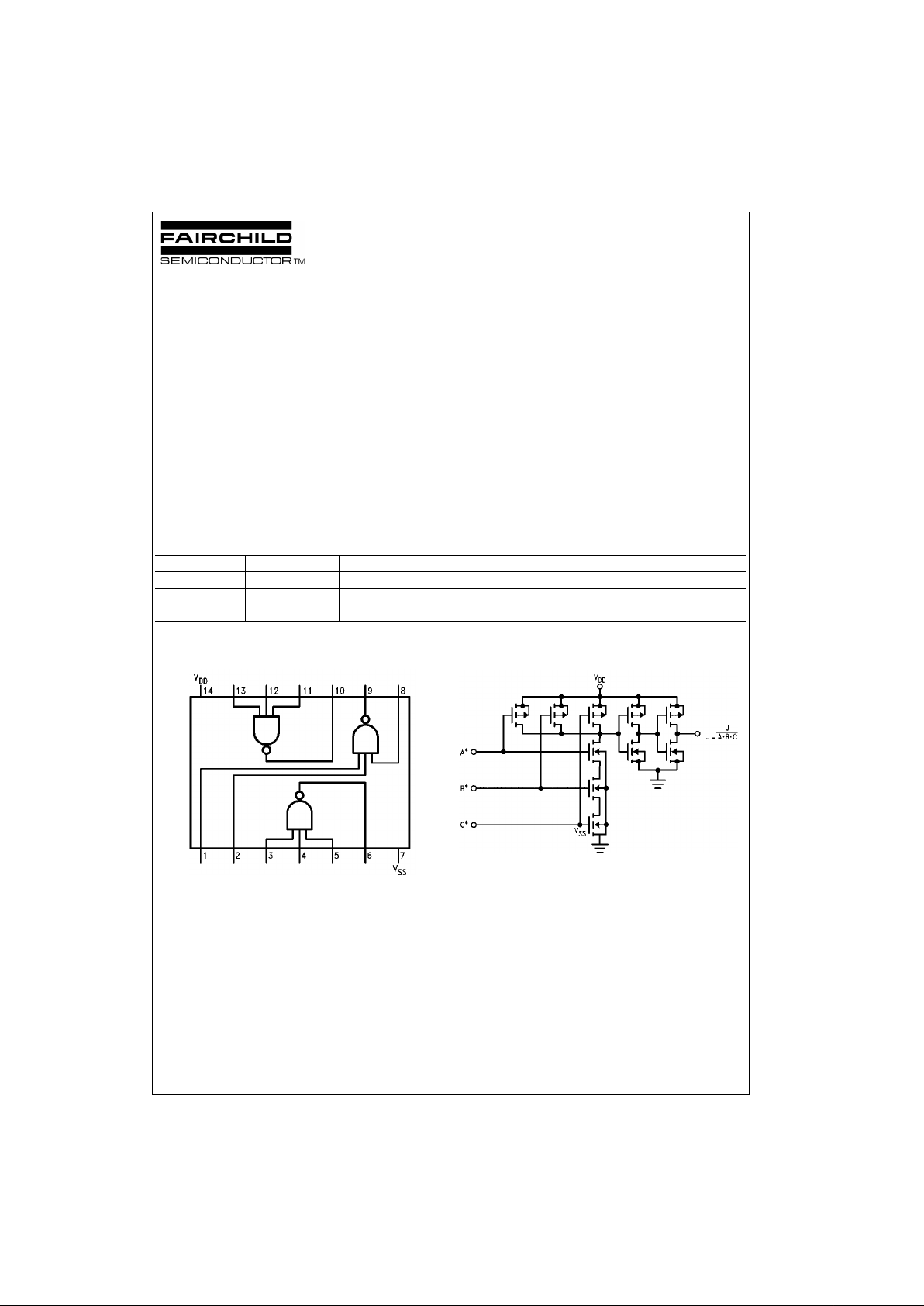
Connection Diagram
Top View
Block Diagram
1
/3 Device Shown
*All Inputs Protected by Standard CMOS Input Protection Circuit.
Order Number Package Number Package Description
CD4023BCM M14A 14-Lead Small Outline Integrated Circuit (SOIC), JEDEC MS-120, 0.150 Narrow
CD4023BCS M14D 14-Lead Small Outline Package (SOP), EIAJ TYPE II, 5.3mm Wide
CD4023BCN N14A 14-Lead Plastic Dual-In-Line Package (PDIP), JEDEC MS-001, 0.300 Wide
Page 2
www.fairchildsemi.com 2
CD4023BC
Absolute Maximum Ratings(Note 1)
(Note 2)
Recommended Operating
Conditions
Note 1: “Absolute Maximum Ratings” are those values beyond which the
safety of the device cannot be guaranteed; they are not meant to imply that
the devices should be operated at these limits. The table of “Recom-
mended Operating Conditions” and “Electrical Characteristics” provides
conditions for actua l device operation.
Note 2: V
SS
= 0V unless otherwise specified.
DC Electrical Characteristics (Note 3)
Note 3: VSS = 0V unless otherwise s pec if ied.
Note 4: I
OH
and IOL are tested one out put at a time.
DC Supply Voltage (VDD) −0.5 VDCto +18 V
DC
Input Voltage (VIN) −0.5 VDCto V
DD
+0.5 V
DC
Storage Temp. Range (TS) −65°C to +150°C
Power Dissipation (P
D
)
Dual-In-Line 700 mW
Small Outline 500 mW
Lead Temperature (T
L
)
(Soldering, 10 seconds) 260
°C
DC Supply Voltage (V
DD
)5 V
DC
to 15 V
DC
Input Voltage (VIN)0 V
DC
to VDD V
DC
Operating Temperature Range (TA) −40°C to +85°C
Symbol Parameter Conditions
−40°C +25°C +85°C
Units
Min Typ Min Typ Max Min Max
I
DD
Quiescent Device Current VDD = 5V 1.0 0.004 1.0 7.5
µAVDD = 10V 2.0 0.005 2.0 15
VDD = 15V 4.0 0.006 4.0 30
V
OL
LOW Level Output Voltage VDD = 5V 0.05 0 0.05 0.05
VVDD = 10V 0.05 0 0.05 0.05
VDD = 15V 0.05 0 0.05 0.05
V
OH
HIGH Level Output Voltage VDD = 5V 4.95 4.95 5 4.95
VVDD = 10V 9.95 9.95 10 9.95
VDD = 15V 14.95 14.95 15 14.95
V
IL
LOW Level Input Voltage VDD=5V, VO=4.5V 1.5 2 1.5 1.5
VVDD=10V, VO=9.0V |IO|<1µA 3.0 4 3.0 3.0
VDD=15V, VO=13.5V 4.0 6 4.0 4.0
V
IH
HIGH Level Input Voltage VDD=5V, VO=0.5V 3.5 3.5 3 3.5
VV
DD
=10V, VO=1.0V |IO|<1µA 7 .0 7.0 6 7.0
VDD=15V, VO=1.5V 11.0 11.0 9 11.0
I
OL
LOW Level Output Current VDD=5V, VO = 0.4V 0.52 0.44 0.88 0.36
mA(Note 4) V
DD
= 10V, VO = 0.5V 1.3 1.1 2.2 0.90
VDD = 15V, VO = 1.5V 3.6 3.0 8 2.4
I
OH
HIGH Level Output Current VDD = 5V, VO = 4.6V −0.52 −0.44 −0.88 −0.36
mA(Note 4) V
DD
= 10V, VO = 9.5V −1.3 −1.1 −2.2 −0.90
VDD = 15V, VO = 13.5V −3.6 −3.0 −8 −2.4
I
IN
Input Current VDD = 15V, VIN = 0V −0.3 −10−5−0.3 −1.0
µA
VDD = 15V, VIN = 15V 0.3 10−50.3 1.0
Page 3

3 www.fairchildsemi.com
CD4023BC
AC Electrical Characteristics (Note 5)
T
A
= 25°C, CL = 50 pF, R
L
= 200k, unless otherwise specified
Note 5: AC Parameters are guar ant eed by DC correlated te s tin g.
Note 6: C
PD
determines the no load AC power consumption of any CMOS device.
For complete explanation, see Family Characteristics Application Note AN-90.
Symbol Parameter Conditions Min Typ Max Units
t
PHL
Propagation Delay, HIGH-to-LOW Level VDD = 5V 130 250
nsVDD = 10V 60 100
V
DD
= 15V 40 70
t
PLH
Propagation Delay, LOW-to-HIGH Level VDD = 5V 110 250
nsVDD = 10V 50 100
V
DD
= 15V 35 70
t
THL
, Transition Time VDD = 5V 90 200
nst
TLH
VDD = 10V 50 100
V
DD
= 15V 40 80
C
IN
Average Input Capacitance Any Input 5 7.5 pF
C
PD
Power Dissipation Capacity (Note 6) Any Gate 17 pF
Page 4

www.fairchildsemi.com 4
CD4023BC
Physical Dimensions inches (millimeters) unless otherwise noted
14-Lead Small Outline Integrated Circuit (SOIC), JEDEC MS-120, 0.150 Narrow
Package Number M14A
Page 5

5 www.fairchildsemi.com
CD4023BC
Physical Dimensions inches (millimeters) unless otherwise noted (Continued)
14-Lead Small Outline Package (SOP), EIAJ TYPE II, 5.3mm Wide
Package Number M14D
Page 6

www.fairchildsemi.com 6
CD4023BC Buffered Triple 3-Input NAND Gate
Physical Dimensions inches (millimeters) unless otherwise noted (Continued)
14-Lead Plastic Dual-In-Line Package (PDIP), JEDEC MS-001, 0.300 Wide
Package Number N14A
Fairchild does not assume any responsibility for use of any circuitr y described, no circuit patent licenses are implied and
Fairchild reserves the right at any time without notice to change said circuitry and specifications.
LIFE SUPPORT POLICY
FAIRCHILD’S PRODUCTS ARE NOT AUTHORIZED FOR USE AS CRITICAL COMPONENTS IN LIFE SUPPORT
DEVICES OR SYSTEMS WITHOUT THE EXPRESS WRITTEN APPROVAL OF THE PRESIDENT OF FAIRCHILD
SEMICONDUCTOR CORPORATION. As used herein:
1. Life supp or t de vices o r systems a re devices or syste ms
which, (a) are intended for surgical implant into the
body, or (b) support or sustain life, and (c) whose failure
to perform when properly used in accordance with
instructions for use provided in the labeling, can be reasonably expected to result in a significant inju ry to the
user.
2. A cr itical compon ent in any compon ent of a life su pport
device or system whose failure t o perform can be reasonably expected to ca use the failure of the life supp ort
device or system, or to affect its safety or effectiveness.
www.fairchildsemi.com
 Loading...