

Datasheet CD4020BCC2, CD4019BCSJX, CD4019BCSJ, CD4019BCN, CD4019BCMX Datasheet (Fairchild Semiconductor)
...Page 1
October 1987
Revised January 1999
CD4019BC Quad AND-OR Select Gate
© 1999 Fairchild Semiconductor Corporation DS005952.prf www.fairchildsemi.com
CD4019BC
Quad AND-OR Select Gate
General Description
The CD4019BC is a complementar y MOS quad AND-OR
select gate. Low power and high noise margin over a wide
voltage range is possible through implementation of N- and
P-channel enhancement m ode transistors. These comp lementary MOS (CMOS) transistors provide the building
blocks for the 4 “AND-OR select” gate configuration s, each
consisting of two 2-input AND gates driving a single 2-input
OR gate. Selection is accompl ished by control bi ts K
A
and
K
B
. All inputs are protecte d against static discharge dam-
age.
Features
■ Wide supply voltage range: 3.0V to 15V
■ High noise immunity: 0.45 V
DD
(typ.)
■ Low power TTL compatibility: Fan out of 2 driving 74L
or 1 driving 74LS
Applications
• AND-OR select gating
• Shift-right/shift-left registers
• True/complement selection
• AND/OR/EXCLUSIVE-OR selection
Ordering Code:
Devices also available in Tape and Reel. Specify by appending the suffix letter “X” to t he ordering code.
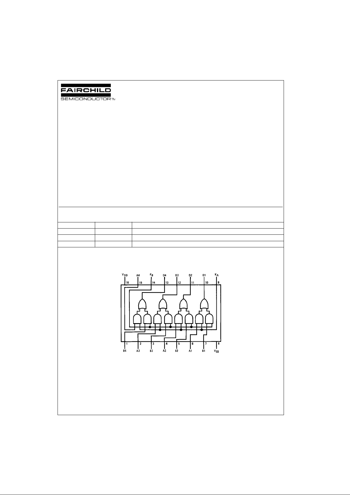
Connection Diagram
Pin Assignments for DIP, SOIC and SOP
Top View
Order Number Package Number Package Description
CD4019BCM M16A 16-Lead Small Outline Integrated Circuit (SOIC), JEDEC MS-012, 0.150” Narrow
CD4019BCSJ M16D 16-Lead Small Outline Package (SOP), EIAJ TYPE II, 5.3mm Wide
CD4019BCN N16E 16-Lead Plastic Dual-In-Line Package (PDIP), JEDEC MS-001, 0.300” Wide
Page 2
www.fairchildsemi.com 2
CD4019BC
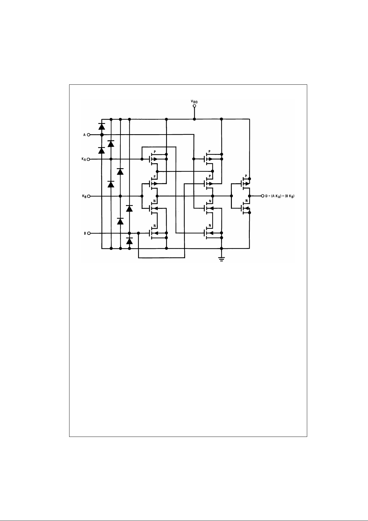
Schematic Diagram
Schematic diagram for 1 of 4 identical stages
Page 3

3 www.fairchildsemi.com
CD4019BC
Absolute Maximum Ratings(Note 1)
(Note 2)
Recommended Operation
Conditions
(Note 2)
Note 1: “Absolute Maximum Rat ings” are tho se values beyond which the
safety of the device cannot be guaranteed; they are not meant to imply that
the devices should be o perated at these limits. The tables of “R ecommended Operating Conditions” and “Electrical Characteristics” provide conditions for actual device operat ion.
Note 2: V
SS
= 0V unless otherw is e s pecified.
DC Electrical Characteristics (Note 3)
Note 3: VSS = 0V unless otherwise specified.
Note 4: I
OH
and IOL are tested one output at a ti m e.
Supply Voltage (VDD) −0.5V to +18V
Input Voltage (V
IN
) −0.5V to VDD +0.5V
Storage Temperature Range (T
S
) −65°C to +150°C
Power Dissipation (P
D
)
Dual-In-Line 700 mW
Small Outline 500 mW
Lead Temperature (T
L
)
(Soldering, 10 seconds ) 260°C
DC Supply Voltage (V
DD
) +3V to +15V
Input Voltage (V
IN
)0V to V
DD
V
Operating Temperature Range (T
A
) −40°C to +85°C
Symbol Parameter Conditions
−40°C +25°C +85°C
Units
Min Max Min Typ Max Min Max
I
DD
Quiescent Device VDD = 5V 1 0.03 1 7.5 µA
Current VDD = 10V 2 0.05 2 15 µA
VDD = 15V 4 0.07 4 30 µA
V
OL
LOW Level |IO| < 1 µA
Output Voltage VDD = 5V 0.05 0 0.05 0.05 V
VDD = 10V 0.05 0 0.05 0.05 V
VDD = 15V 0.05 0 0.05 0.05 V
V
OH
HIGH Level |IO| < 1 µA
Output Voltage VDD = 5V 4.95 4.95 5 4.95 V
VDD = 10V 9.95 9.95 10 9.95 V
VDD = 15V 14.95 14.95 15 14.95 V
V
IL
LOW Level VDD = 5V, VO = 0.5V or 4.5V 1.5 2 1.5 1.5 V
Input Voltage VDD = 10V, VO = 1.0V or 9.0V 3.0 4 3.0 3.0 V
VDD = 15V, VO = 1.5V or 13.5V 4.0 6 4.0 4.0 V
V
IH
HIGH Level VDD = 5V, VO = 0.5V or 4.5V 3.5 3.5 3 3.5 V
Input Voltage VDD = 10V, VO = 1.0V or 9.0V 7.0 7.0 6 7.0 V
VDD = 15V, VO = 1.5V or 13.5V 11.0 11.0 9 11.0 V
I
OL
LOW Level Output VDD = 5V, VO = 0.4V 0.52 0.44 1 0.36 mA
Current (Note 4) VDD = 10V, VO = 0.5V 1.3 1.1 2.5 0.9 mA
VDD = 15V, VO = 1.5V 3.6 3.0 10 2.4 mA
I
OH
HIGH Level Output VDD = 5V, VO = 4.6V −0.2 −0.16 −0.4 −0.12 mA
Current (Note 4) VDD = 10V, VO = 9.5V −0.5 −0.4 −1.0 −0.3 mA
VDD = 15V, VO = 13.5V −1.4 −1.2 −3.0 −1.0 mA
I
IN
Input Current VDD = 15V, VIN = 0V −0.30 −10−5−0.30 −1.0 µA
VDD = 15V, VIN = 15V 0.30 10−50.30 1.0 µA
Page 4

www.fairchildsemi.com 4
CD4019BC
AC Electrical Charac teristics (Note 5)
TA = 25°C, CL = 50 pF, RL = 200k, unless otherwise specified
Note 5: AC Parameters are guara nt eed by DC correlated testing.
Symbol Parameter Conditions Min Typ Max Units
t
PHL
, Propagation Delay, VDD = 5V 100 300 ns
t
PLH
Input to Output VDD = 10V 50 120 ns
VDD = 15V 45 100 ns
t
THL
HIGH-to-LOW Level VDD = 5V 100 200 ns
Transition Time VDD = 10V 50 100 ns
VDD = 15V 40 80 ns
t
TLH
LOW-to-HIGH Level VDD = 5V 150 300 ns
Transition Time VDD = 10V 70 140 ns
VDD = 15V 50 100 ns
C
IN
Input Capacitance All A and B Inputs 5 7.5 pF
KA and KB Inputs 10 15 pF
Page 5

5 www.fairchildsemi.com
CD4019BC
Physical Dimensions inches (millimeters) unless otherwise noted
16-Lead Small Outline Integrated Circuit (SOIC), JEDEC MS-012, 0.150” Narrow
Package Number M16A
16-Lead Small Outline Package (SOP), EIAJ TYPE II, 5.3mm Wide
Package Number M16D
Page 6

Fairchild does not assume any responsibility for use of any circuitry described, no circuit patent licenses are implied and Fairchild reser ves the right at any time without notice to change said circuitry and specifications.
CD4019BC Quad AND-OR Select Gate
LIFE SUPPORT POLICY
FAIRCHILD’S PRODUCTS ARE NOT AUTHORIZED FOR USE AS CRITICAL COMPONENTS IN LIFE SUPPORT
DEVICES OR SYSTEMS WITHOUT THE EXPRESS WRITTEN APPROVAL OF THE PRESIDENT OF FAIRCHILD
SEMICONDUCTOR CORPORATION. As used herein:
1. Life support devices or system s ar e devices or syste ms
which, (a) are intended for surgical implant into the
body, or (b) support or sustain life, and (c) whose failure
to perform when properly used in accordance with
instructions for use provided in the labeling, can be reasonably expected to result in a significant injury to the
user.
2. A critical component in any c omponent of a life suppor t
device or system whose failure to perform can be reasonably expected to cause the failure of the life suppor t
device or system, or to affect its safety or effectiveness.
www.fairchildsemi.com
Physical Dimensions inches (millimeters) unless otherwise noted (Continued)
16-Lead Plastic Dual-In-Line Package (PDIP), JEDEC MS-001, 0.300” Wide
Package Number N16E
 Loading...