

Page 1
CD40106BMS
December 1992
Features
• High Voltage Type (20V Rating)
• Schmitt Trigger Action with No External Components
• Hysteresis Voltage (Typ.)
- 0.9V at VDD = 5V
- 2.3V at VDD = 10V
- 3.5V at VDD = 15V
• Noise Immunity Greater than 50%
• No Limit on Input Rise and Fall Times
• Low VDD to VSS Current During Slow Input Ramp
• 100% Tested for Quiescent Current at 20V
• 5V, 10V and 15V Parametric Ratings
• Maximum Input Current of 1µA at 18V Over Full Pack-
age Temperature Range; 100nA at 18V and +25
• Standardized Symmetrical Output Characteristics
• Meets All Requirements of JEDEC Tentative Standard
No. 13B, “Standard Specifications for Description of
‘B’ Series CMOS Devices”
CMOS Hex Schmitt Triggers
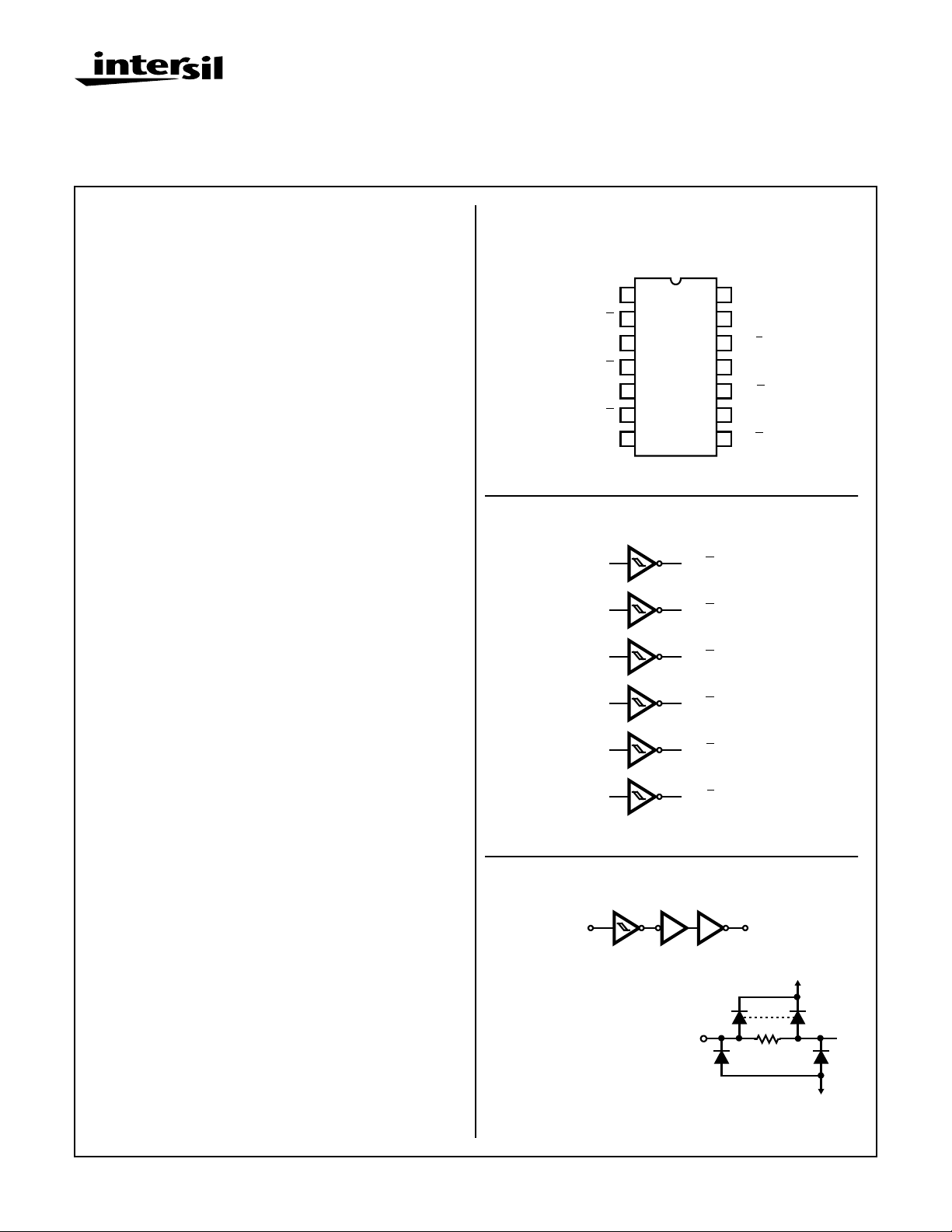
Pinout
CD40106BMS
TOP VIEW
A
1
A
2
G =
3
B
B
4
H =
5
C
C
6
I =
VSS
7
o
C
Functional Diagram
1
A
3
B
2
G =
4
H =
VDD
14
F
13
F
12
L =
11
E
E
10
K =
D
9
J =
D
8
A
B
Applications
• Wave and Pulse Shapers
• High Noise Environment Systems
• Monostable Multivibrators
• Astable Multivibrators
Description
CD40106BMS consists of six Schmitt trigger circuits. Each
circuit functions as an inverter with Schmitt trigger action on
the input. The trigger switches at different points for positive
and negative going signals. The difference between the
positive going voltage (VP) and the negative going voltage
(VN) is defined as hysteresis voltage (VH) (see Figure 17).
The CD40106BMS is supplied in these 14 lead outline
packages:
Braze Seal DIP H4Q
Frit Seal DIP H1B
Ceramic Flatpack H3W
C
D
E
F
Logic Diagram
*
1 (3, 5, 9, 11, 13)
ALL INPUTS ARE PROTECTED
*
BY CMOS PROTECTION
NETWORK
A
5
9
11
13
6
I =
C
8
J =
D
10
K =
E
12
L =
F
*
G
2 (4, 6, 8, 10, 12)
VDD
FIGURE 1. 1 OF 6 SCHMITT TRIGGERS
CAUTION: These devices are sensitive to electrostatic discharge; follow proper IC Handling Procedures.
1-888-INTERSIL or 321-724-7143 | Copyright © Intersil Corporation 1999
7-1327
File Number
VSS
3354
Page 2
Specifications CD40106BMS
Absolute Maximum Ratings Reliability Information
DC Supply Voltage Range, (VDD) . . . . . . . . . . . . . . . -0.5V to +20V
(Voltage Referenced to VSS Terminals)
Input Voltage Range, All Inputs . . . . . . . . . . . . .-0.5V to VDD +0.5V
DC Input Current, Any One Input . . . . . . . . . . . . . . . . . . . . . . . .±10mA
Operating Temperature Range. . . . . . . . . . . . . . . . -55oC to +125oC
Package Types D, F, K, H
Storage Temperature Range (TSTG). . . . . . . . . . . -65oC to +150oC
Lead Temperature (During Soldering) . . . . . . . . . . . . . . . . . +265oC
At Distance 1/16 ± 1/32 Inch (1.59mm ± 0.79mm) from case for
10s Maximum
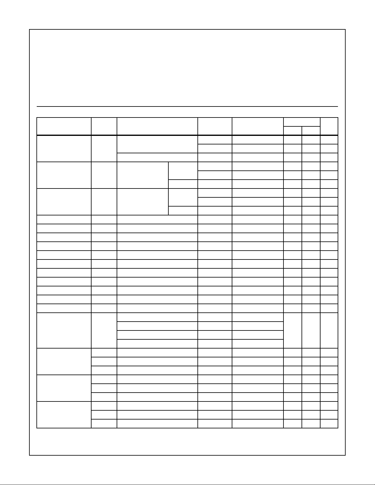
TABLE 1. DC ELECTRICAL PERFORMANCE CHARACTERISTICS
PARAMETER SYMBOL CONDITIONS (NOTE 1)
Supply Current IDD VDD = 20V, VIN = VDD or GND 1 +25oC-2µA
VDD = 18V, VIN = VDD or GND 3 -55oC-2µA
Input Leakage Current IIL VIN = VDD or GND VDD = 20 1 +25oC -100 - nA
VDD = 18V 3 -55oC -100 - nA
Input Leakage Current IIH VIN = VDD or GND VDD = 20 1 +25oC - 100 nA
VDD = 18V 3 -55oC - 100 nA
Output Voltage VOL15 VDD = 15V, No Load 1, 2, 3 +25oC, +125oC, -55oC - 50 mV
Output Voltage VOH15 VDD = 15V, No Load (Note 2) 1, 2, 3 +25oC, +125oC, -55oC 14.95 - V
Output Current (Sink) IOL5 VDD = 5V, VOUT = 0.4V 1 +25oC 0.53 - mA
Output Current (Sink) IOL10 VDD = 10V, VOUT = 0.5V 1 +25oC 1.4 - mA
Output Current (Sink) IOL15 VDD = 15V, VOUT = 1.5V 1 +25oC 3.5 - mA
Output Current (Source) IOH5A VDD = 5V, VOUT = 4.6V 1 +25oC - -0.53 mA
Output Current (Source) IOH5B VDD = 5V, VOUT = 2.5V 1 +25oC - -1.8 mA
Output Current (Source) IOH10 VDD = 10V, VOUT = 9.5V 1 +25oC - -1.4 mA
Output Current (Source) IOH15 VDD = 15V, VOUT = 13.5V 1 +25oC - -3.5 mA
N Threshold Voltage VNTH VDD = 10V, ISS = -10µA 1 +25oC -2.8 -0.7 V
P Threshold Voltage VPTH VSS = 0V, IDD = 10µA 1 +25oC 0.7 2.8 V
Functional F VDD = 2.8V, VIN = VDD or GND 7 +25oC VOH >
VDD = 20V, VIN = VDD or GND 7 +25oC
VDD = 18V, VIN = VDD or GND 8A +125oC
VDD = 3V, VIN = VDD or GND 8B -55oC
Positive Trigger
Threshold Voltage
(See Figure 17)
Negative Trigger
Threshold Voltage
(See Figure 17)
Hysteresis Voltage
(See Figure 17)
NOTES: 1. All voltages referenced to device GND, 100% testing being
implemented.
2. Go/No Go test with limits applied to inputs.
VP5 VDD = 5V 1, 2, 3 +25oC, +125oC, -55oC 2.2 3.6 V
VP10 VDD = 10V 1, 2, 3 +25oC, +125oC, -55oC 4.6 7.1 V
VP15 VDD = 15V 1, 2, 3 +25oC, +125oC, -55oC 6.8 10.8 V
VN5 VDD = 5V 1, 2, 3 +25oC, +125oC, -55oC 0.9 2.8 V
VN10 VDD = 10V 1, 2, 3 +25oC, +125oC, -55oC 2.5 5.2 V
VN15 VDD = 15V 1, 2, 3 +25oC, +125oC, -55oC 4 7.4 V
VH5 VDD = 5V 1, 2, 3 +25oC, +125oC, -55oC 0.3 1.6 V
VH10 VDD = 10V 1, 2, 3 +25oC, +125oC, -55oC 1.2 3.4 V
VH15 VDD = 15V 1, 2, 3 +25oC, +125oC, -55oC 1.6 5.0 V
Thermal Resistance . . . . . . . . . . . . . . . . θ
Ceramic DIP and FRIT Package. . . . . 80oC/W 20oC/W
Flatpack Package . . . . . . . . . . . . . . . . 70oC/W 20oC/W
Maximum Package Power Dissipation (PD) at +125oC
For TA = -55oC to +100oC (Package Type D, F, K) . . . . . .500mW
For TA = +100oC to +125oC (Package Type D, F, K). . . . . .Derate
Linearity at 12mW/oC to 200mW
Device Dissipation per Output Transistor . . . . . . . . . . . . . . . 100mW
For TA = Full Package Temperature Range (All Package Types)
Junction Temperature . . . . . . . . . . . . . . . . . . . . . . . . . . . . . . +175oC
GROUP A
SUBGROUPS TEMPERATURE
2 +125oC - 200 µA
2 +125oC -1000 - nA
2 +125oC - 1000 nA
3. For accuracy, voltage is measured differentially to VDD. Limit
is 0.050V max.
ja
LIMITS
VDD/2
VOL <
VDD/2
θ
jc
UNITSMIN MAX
V
7-1328
Page 3
Specifications CD40106BMS
TABLE 2. AC ELECTRICAL PERFORMANCE CHARACTERISTICS
GROUP A
PARAMETER SYMBOL CONDITIONS (NOTE 1, 2)
Propagation Delay TPHL
TPLH
Transition Time TTHL
TTLH
NOTES:
1. CL = 50pF, RL = 200K, Input TR, TF < 20ns
2. -55oC and +125oC limits guaranteed, 100% testing being implemented.
PARAMETER SYMBOL CONDITIONS NOTES TEMPERATURE
Supply Current IDD VDD = 5V, VIN = VDD or GND 1, 2 -55oC, +25oC- 1 µA
Output Voltage VOL VDD = 5V, No Load 1, 2 +25oC, +125oC,
Output Voltage VOL VDD = 10V, No Load 1, 2 +25oC, +125oC,
Output Voltage VOH VDD = 5V, No Load 1, 2 +25oC, +125oC,
Output Voltage VOH VDD = 10V, No Load 1, 2 +25oC, +125oC,
Output Current (Sink) IOL5 VDD = 5V, VOUT = 0.4V 1, 2 +125oC 0.36 - mA
Output Current (Sink) IOL10 VDD = 10V, VOUT = 0.5V 1, 2 +125oC 0.9 - mA
Output Current (Sink) IOL15 VDD = 15V, VOUT = 1.5V 1, 2 +125oC 2.4 - mA
Output Current (Source) IOH5A VDD = 5V, VOUT = 4.6V 1, 2 +125oC - -0.36 mA
Output Current (Source) IOH5B VDD = 5V, VOUT = 2.5V 1, 2 +125oC - -1.15 mA
Output Current (Source) IOH10 VDD = 10V, VOUT = 9.5V 1, 2 +125oC - -0.9 mA
Output Current (Source) IOH15 VDD =15V, VOUT = 13.5V 1, 2 +125oC - -2.4 mA
Propagation Delay TPHL
TPLH
Transition Time TTHL
TTLH
VDD = 5V, VIN = VDD or GND 9 +25oC - 280 ns
VDD = 5V, VIN = VDD or GND 9 +25oC - 200 ns
TABLE 3. ELECTRICAL PERFORMANCE CHARACTERISTICS
VDD = 10V, VIN = VDD or GND 1, 2 -55oC, +25oC- 2 µA
VDD = 15V, VIN = VDD or GND 1, 2 -55oC, +25oC- 2 µA
VDD = 10V 1, 2, 3 +25oC - 140 ns
VDD = 15V 1, 2, 3 +25oC - 120 ns
VDD = 10V 1, 2, 3 +25oC - 100 ns
VDD = 15V 1, 2, 3 +25oC - 80 ns
SUBGROUPS TEMPERATURE
10, 11 +125oC, -55oC - 378 ns
10, 11 +125oC, -55oC - 270 ns
+125oC-30µA
+125oC-60µA
+125oC - 120 µA
-55oC
-55oC
-55oC
-55oC
-55oC 0.64 - mA
-55oC 1.6 - mA
-55oC 4.2 - mA
-55oC - -0.64 mA
-55oC - -2.0 mA
-55oC - -1.6 mA
-55oC - -4.2 mA
LIMITS
UNITSMIN MAX
LIMITS
UNITSMIN MAX
-50mV
-50mV
4.95 - V
9.95 - V
7-1329
Page 4

Specifications CD40106BMS
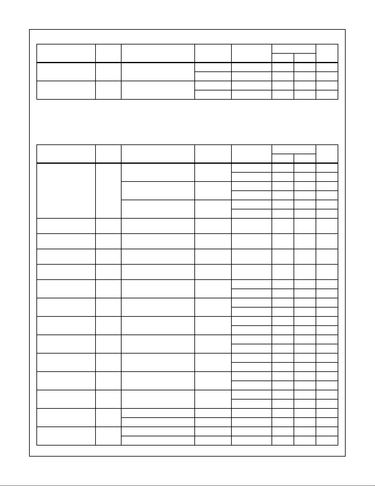
TABLE 3. ELECTRICAL PERFORMANCE CHARACTERISTICS (Continued)
LIMITS
PARAMETER SYMBOL CONDITIONS NOTES TEMPERATURE
Input Capacitance CIN Any Input 1, 2 +25oC - 7.5 pF
NOTES:
1. All voltages referenced to device GND.
2. The parameters listed on Table 3 are controlled via design or process and are not directly tested. These parameters are characterized on
initial design release and upon design changes which would affect these characteristics.
3. CL = 50pF, RL = 200K., Input TR, TF < 20ns
TABLE 4. POST IRRADIATION ELECTRICAL PERFORMANCE CHARACTERISTICS
LIMITS
PARAMETER SYMBOL CONDITIONS NOTES TEMPERATURE
Supply Current IDD VDD = 20V, VIN = VDD or GND 1, 4 +25oC - 7.5 µA
N Threshold Voltage VNTH VDD = 10V, ISS = -10µA 1, 4 +25oC -2.8 -0.2 V
N Threshold Voltage
Delta
P Threshold Voltage VTP VSS = 0V, IDD = 10µA 1, 4 +25oC 0.2 2.8 V
P Threshold Voltage
Delta
Functional F VDD = 18V, VIN = VDD or GND 1 +25oC VOH >
Propagation Delay Time TPHL
NOTES: 1. All voltages referenced to device GND.
2. CL = 50pF, RL = 200K, Input TR, TF < 20ns.
∆VTN VDD = 10V, ISS = -10µA 1, 4 +25oC-±1V
∆VTP VSS = 0V, IDD = 10µA 1, 4 +25oC-±1V
VOL <
TPLH
VDD = 3V, VIN = VDD or GND
VDD = 5V 1, 2, 3, 4 +25oC - 1.35 x
3. See Table 2 for +25oC limit.
4. Read and Record
VDD/2
VDD/2
+25oC
Limit
UNITSMIN MAX
UNITSMIN MAX
V
ns
TABLE 5. BURN-IN AND LIFE TEST DELTA PARAMETERS +25oC
PARAMETER SYMBOL DELTA LIMIT
Supply Current - MSI-1 IDD ± 0.2µA
Output Current (Sink) IOL5 ± 20% x Pre-Test Reading
Output Current (Source) IOH5A ± 20% x Pre-Test Reading
TABLE 6. APPLICABLE SUBGROUPS
MIL-STD-883
CONFORMANCE GROUP
Initial Test (Pre Burn-In) 100% 5004 1, 7, 9 IDD, IOL5, IOH5A
Interim Test 1 (Post Burn-In) 100% 5004 1, 7, 9 IDD, IOL5, IOH5A
Interim Test 2 (Post Burn-In) 100% 5004 1, 7, 9 IDD, IOL5, IOH5A
PDA (Note 1) 100% 5004 1, 7, 9, Deltas
Interim Test 3 (Post Burn-In) 100% 5004 1, 7, 9 IDD, IOL5, IOH5A
PDA (Note 1) 100% 5004 1, 7, 9, Deltas
Final Test 100% 5004 2, 3, 8A, 8B, 10, 11
Group A Sample 5005 1, 2, 3, 7, 8A, 8B, 9, 10, 11
METHOD GROUP A SUBGROUPS READ AND RECORD
7-1330
Page 5

Specifications CD40106BMS
TABLE 6. APPLICABLE SUBGROUPS
MIL-STD-883
CONFORMANCE GROUP
Group B Subgroup B-5 Sample 5005 1, 2, 3, 7, 8A, 8B, 9, 10, 11, Deltas Subgroups 1, 2, 3, 9, 10, 11
Subgroup B-6 Sample 5005 1, 7, 9
Group D Sample 5005 1, 2, 3, 8A, 8B, 9 Subgroups 1, 2 3
NOTE: 1. 5% Parameteric, 3% Functional; Cumulative for Static 1 and 2.
CONFORMANCE GROUPS
Group E Subgroup 2 5005 1, 7, 9 Table 4 1, 9 Table 4
FUNCTION OPEN GROUND VDD 9V ± -0.5V
Static Burn-In 1
2, 4, 6, 8, 10, 12 1, 3, 5, 7, 9, 11, 13 14
Note 1
Static Burn-In 2
2, 4, 6, 8, 10, 12 7 1, 3, 5, 9, 11,
Note 1
Dynamic Burn-
- 7 14 2, 4, 6, 8, 10, 12 1, 3, 5, 9, 11, 13
In Note 1
Irradiation
2, 4, 6, 8, 10, 12 7 1, 3, 5, 9, 11,
Note 2
NOTES:
1. Each pin except VDD and GND will have a series resistor of 10K ± 5%, VDD = 18V ± 0.5V
2. Each pin except VDD and GND will have a series resistor of 47K ± 5%; Group E, Subgroup 2, sample size is 4 dice/wafer, 0 failures,
VDD = 10V ± 0.5V
METHOD GROUP A SUBGROUPS READ AND RECORD
TABLE 7. TOTAL DOSE IRRADIATION
MIL-STD-883
METHOD
PRE-IRRAD POST-IRRAD PRE-IRRAD POST-IRRAD
TEST READ AND RECORD
TABLE 8. BURN-IN AND IRRADIATION TEST CONNECTIONS
OSCILLATOR
50kHz 25kHz
13, 14
13, 14
Typical Performance Characteristics
AMBIENT TEMPERATURE (TA) = +25oC
30
25
20
15
10
5
OUTPUT LOW (SINK) CURRENT (IOL) (mA)
0 5 10 15
FIGURE 2. TYPICAL OUTPUT LOW (SINK) CURRENT
GATE-TO-SOURCE VOLTAGE (VGS) = 15V
10V
5V
DRAIN-TO-SOURCE VOLTAGE (VDS) (V)
CHARACTERISTICS
AMBIENT TEMPERATURE (TA) = +25oC
15.0
12.5
10.0
7.5
5.0
2.5
OUTPUT LOW (SINK) CURRENT (IOL) (mA)
0 5 10 15
GATE-TO-SOURCE VOLTAGE (VGS) = 15V
10V
5V
DRAIN-TO-SOURCE VOLTAGE (VDS) (V)
FIGURE 3. MINIMUM OUTPUT LOW (SINK) CURRENT
CHARACTERISTICS
7-1331
Page 6

Specifications CD40106BMS
Typical Performance Characteristics (Continued)
DRAIN-TO-SOURCE VOLTAGE (VDS) (V)
0-5-10-15
AMBIENT TEMPERATURE (TA) = +25oC
GATE-TO-SOURCE VOLTAGE (VGS) = -5V
-10V
-15V
0
-5
-10
-15
-20
-25
-30
FIGURE 4. TYPICAL OUTPUT HIGH (SOURCE) CURRENT
CHARACTERISTICS
AMBIENT TEMPERATURE (TA) = +25oC
SUPPLY VOLTAGE (VDD) = 15V
15.0
CURRENT
12.5
10.0
CURRENT
7.5
5.0
OUTPUT VOLTAGE (VO) (V)
PEAK
10V
PEAK
5V
VIN
VO
VDD
ALL
ID
OTHER
INPUTS TO
VDD OR VSS
2
VO
1
ID
DRAIN-TO-SOURCE VOLTAGE (VDS) (V)
AMBIENT TEMPERATURE (TA) = +25oC
GATE-TO-SOURCE VOLTAGE (VGS) = -5V
-15V
OUTPUT HIGH (SOURCE) CURRENT (IOH) (mA)
FIGURE 5. MINIMUM OUTPUT HIGH (SOURCE) CURRENT
CHARACTERISTICS
1.5
1.0
0.5
DRAIN CURRENT (ID) (mA)
SUPPLY VOLTAGE (VDD) = 15V
15
10
5
OUTPUT VOLTAGE (VO) (V)
10V
5V
-10V
-55oC
+125
VIN
0-5-10-15
0
-5
-10
-15
OUTPUT HIGH (SOURCE) CURRENT (IOH) (mA)
VDD
1
o
C
2
VO
ALL
OTHER
INPUTS TO
VDD OR VSS
2.5
0
INPUT VOLTAGE (VI) (V)
15.012.510.07.55.02.50
0
FIGURE 6. TYPICAL CURRENT AND VOLTAGE TRANSFER
CHARACTERISTICS
200
AMBIENT TEMPERATURE (TA) = +25oC
150
100
50
PROPAGATION TIME (tPHL, tPLH) (ns)
0
0 40 60 80 10020
SUPPLY VOLTAGE (VDD) = 5V
10V
5V
LOAD CAPACITANCE (CL) (pF)
FIGURE 8. TYPICAL PROPAGATION DELAY TIME AS A FUNC-
TION OF LOAD CAPACITANCE
0
INPUT VOLTAGE (VI) (V)
151050
FIGURE 7. TYPICAL VOLTAGE TRANSFER CHARACTERIS-
TICS AS A FUNCTION OF TEMPERATURE
AMBIENT TEMPERATURE (TA) = +25oC
200
150
100
50
TRANSITION TIME (tTHL, tTLH) (ns)
0
SUPPLY VOLTAGE (VDD) = 5V
10V
15V
0 40 60 80 10020
LOAD CAPACITANCE (CL) (pF)
FIGURE 9. TYPICAL TRANSITION TIME AS A FUNCTION OF
LOAD CAPACITANCE
7-1332
Page 7

CD40106BMS
Typical Performance Characteristics (Continued)
5
10
8
6
AMBIENT TEMPERATURE (TA) = +25oC
4
2
4
10
8
6
4
2
3
10
8
6
4
2
2
10
8
6
4
2
10
POWER DISSIPATION PER TRIGGER (PD) (µW)
10
FIGURE 10. TYPICAL POWER DISSIPATION PER TRIGGER AS
(
X 100 PERCENT
VH
(
HYSTERESIS
FIGURE 12. TYPICAL PERCENT HYSTERESIS AS A FUNCTION
SUPPLY VOLTAGE (VDD) = 15V
10V
-1
8642
1
8642
10 10
864286428642
2
INPUT FREQUENCY (f) (kHz)
A FUNCTION OF INPUT FREQUENCY
AMBIENT TEMPERATURE (TA) = +25oC
25
20
15
VDD
10
5
0
01015205
SUPPLY VOLTAGE (VDD) (V)
OF SUPPLY VOLTAGE
5V
CL = 50pF
CL = 15pF
3
10
4
10
FIGURE 11. TYPICAL TRIGGER THRESHOLD VOLTAGE AS A
FIGURE 13. TYPICAL POWER DISSIPATION AS A FUNCTION
AMBIENT TEMPERATURE (TA) = +25oC
INPUT ON TERMINALS 1, 5, 8, 12 OR 2, 6, 9, 13;
OTHER INPUTS TIED TO VDD
15
10
5
TRIGGER THRESHOLD VOLTAGE (VP, VN) (V)
0
01015205
SUPPLY VOLTAGE (VDD) (V)
FUNCTION OF SUPPLY VOLTAGE
4
10
8
6
4
2
3
SUPPLY VOLTAGE (VDD) = 15pF
10
8
FREQUENCY (f) = 100kHz
6
4
2
2
15V, 10kHz
10
8
6
4
2
15V, 1kHz
10
8
6
10V, 1kHz
4
2
1
8
POWER DISSIPATION (PD) (µW)
6
5V, 1kHz
4
2
-1
10
0.1
AMBIENT TEMPERATURE (TA) = +25oC
LOAD CAPACITANCE (CL) = 15pF
8642
1
8642
10 10
RISE AND FALL TIME (tr, tf) (ns)
OF RISE AND FALL TIMES
VP
VN
864286428642
2
10
3
4
10
Applications
VDD
VSS
VDD
R
VDD
VDD
VSS
1/3 CD4007UB
C
21
1/6 CD40106BMS
VSS
1/6 CD40106BMS
VSS
tM = RC n
50kΩ≤ R ≤ 1MΩ
FREQUENCY RANGE OF WAVE SHAPE
IS FROM DC TO 1MHz
100pF ≤ C ≤ 1µF
FOR THE RANGE OF R AND C
GIVEN 5µs < tM < 1s
FIGURE 14. WAVE SHAPER FIGURE 15. MONOSTABLE MULTIVIBRATOR
7-1333
tM
VDD
VSS
VDD
VDD-VP
Page 8

Applications (Continued)
VP VN
VDD
CD40106BMS
1/6 CD40106BMS
R
C
VSS
FIGURE 16. ASTABLE MULTIVIBRATOR
tA
VDD
VSS
VDD-VN
tA = RC n
50kΩ≤ R ≤ 1MΩ
100pF ≤ C ≤ 1µF
FOR THE RANGE OF R AND C
GIVEN 2µs < tA < 0.4s
VP
VN
VDD-VP
VIN
VSS
VDD
VO
VSS
VOH
(a) DEFINITION OF VP, VN, VH
FIGURE 17. HYSTERESIS DEFINITION, CHARACTERISTICS, AND TEST SETUP
OUTPUT
CHARACTERISTIC
LOGIC “1”
OUTPUT
REGION
LOGIC “0”
OUTPUT
REGION
VOL
VP
VN
VSS
VDD
VH
INPUT
CHARACTERISTIC
LOGIC “0”
INPUT
REGION
VO
LOGIC “1”
INPUT
REGION
VH
VN
(b) TRANSFER CHARACTERISTIC OF 1 OF 6 GATES
VH = VP - VN
VIN
VP
VOH
VOL
DRIVER LOAD
VIN
VO
FIGURE 18. INPUT AND OUTPUT CHARACTERISTICS
7-1334
Page 9

Chip Dimensions and Pad Layout
CD40106BMS
Dimensions in parenthesis are in millimeters and are
derived from the basic inch dimensions as indicated.
Grid graduations are in mils (10
-3
inch).
METALLIZATION: Thickness: 11kÅ − 14kÅ, AL.
PASSIVATION: 10.4kÅ - 15.6kÅ, Silane
BOND PADS: 0.004 inches X 0.004 inches MIN
DIE THICKNESS: 0.0198 inches - 0.0218 inches
All Intersil semiconductor products are manufactured, assembled and tested under ISO9000 quality systems certification.
Intersil products are sold by description only. Intersil Corporation reserves the right to make changes in circuit design and/or specifications at any time without
notice. Accordingly, the reader is cautioned to verify that data sheets are current before placing orders. Information furnished by Intersil is believed to be accurate
and reliable. However, no responsibility is assumed by Intersil or its subsidiaries for its use; nor for any infringements of patents or other rights of third parties which
may result from its use. No license is granted by implication or otherwise under any patent or patent rights of Intersil or its subsidiaries.
For information regarding Intersil Corporation and its products, see web site http://www.intersil.com
Sales Office Headquarters
NORTH AMERICA
Intersil Corporation
P. O. Box 883, Mail Stop 53-204
Melbourne, FL 32902
TEL: (321) 724-7000
FAX: (321) 724-7240
EUROPE
Intersil SA
Mercure Center
100, Rue de la Fusee
1130 Brussels, Belgium
TEL: (32) 2.724.2111
FAX: (32) 2.724.22.05
ASIA
Intersil (Taiwan) Ltd.
Taiwan Limited
7F-6, No. 101 Fu Hsing North Road
Taipei, Taiwan
Republic of China
TEL: (886) 2 2716 9310
FAX: (886) 2 2715 3029
1335
 Loading...