

Page 1
CD22M3493
/
j
/
/
/
/
/
/
/
[ /Title
()
Sub-
ect ()
Autho
r ()
Key-
words
()
Cre-
ator ()
DOCI
NFO
pdf-
mark
[
Page-
Mode
Use-
Out-
lines
DOC-
VIEW
pdf-
mark
Data Sheet January 1997 File Number
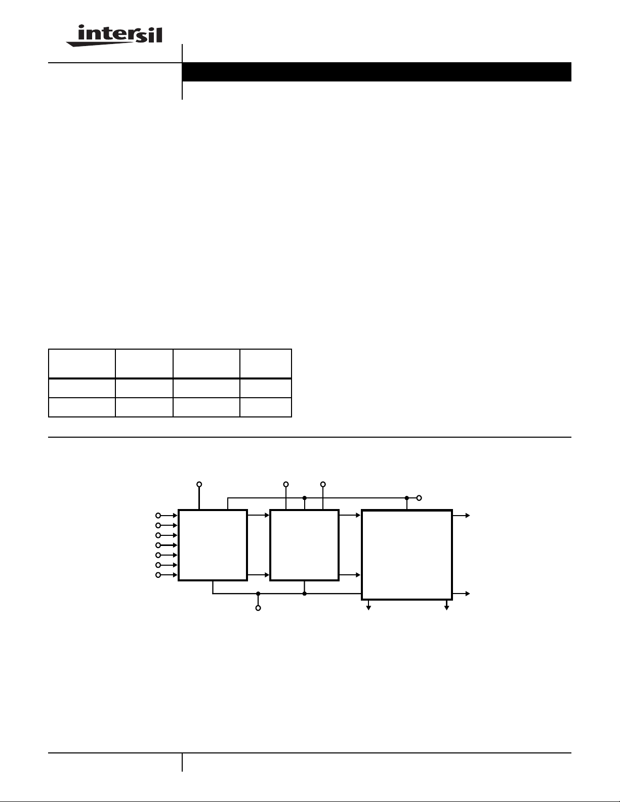
12 x 8 x 1 BiMOS-E Crosspoint Switch
The Intersil CD22M3493 is an array of 96 analog switches
capable of handling signals from DC to video. Because of
the switch structure, input signals may swing through the
total supply voltage range, V
switches may be addressed via the ADDRESS input to the
7 to 96 line decoder. The state of the addressed switch is
established by the signal to the DATA input. A low or logic
zero input will open the switch, while a high logic level or a
one will result in closure of the addressed switch when the
STROBE input goes high from its normally low state. Any
number or combination of connections may be active at
one time. Each connection, however, must be made or
broken individually in the manner previously described. All
switches may be reset by taking the RESET input from a
zero state to a one state and then returning it to its normal
low state.
to VSS. Each of the 96
DD
Ordering Information
TEMP.
PART NUMBER
CD22M3493E -40 to 85 40 Ld PDIP E40.6
CD22M3493Q -40 to 85 44 Ld PLCC N44.65
RANGE (oC) PACKAGE PKG. NO.
Block Diagram
STROBE DATA RESET
AX0
AX1
AX2
AX3
AY0
AY1
AY2
7 TO 96
DECODER
96 96
Features
• 96 Analog Switches
•Low R
• Guaranteed RON Matching
• Analog Signal Input Voltage Equal to the Supply Voltage
• Wide Operating Voltage . . . . . . . . . . . . . . . . . . .4V to 16V
• Parallel Input Addressing
• High Latch Up Current . . . . . . . . . . . . . . . . . . 50mA (Min)
• Very Low Crosstalk
• Pin and Functionally Compatible with the Following Types:
ON
SGS M3493, SGS M093, SSI 78A093A, and Mitel
MT8812
Applications
• PBX Systems
• Instrumentation
• Analog and Digital Multiplexers
• Video Switching Networks
11
LATCHES 12 X 8
SWITCH
ARRAY
2491.4
V
DD
X0 - X11
64
V
SS
CAUTION: These devices are sensitive to electrostatic discharge; follow proper IC Handling Procedures.
http://www.intersil.com or 407-727-9207 | Copyright © Intersil Corporation 1999
Y0 - Y7
Page 2
CD22M3493
Absolute Maximum Ratings Thermal Information
DC Supply Voltage (VDD) (Referenced to VSS . . . . . . .-0.5V to 17V
Supply Voltage Range
For TA = Full Package Temperature Range
VSS = 0V, VDD4V to 16V
DC Input Diode Current, I
IN
For VI < VSS -0.5V or VI > VDD +0.5V. . . . . . . . . . . . . . . . ±20mA
DC Output Diode Current, I
OK
For VO < VSS -0.5V or VO > VDD +0.5V . . . . . . . . . . . . . . ±20mA
DC Transmission Gate Current . . . . . . . . . . . . . . . . . . . . . . . ±25mA
Power Dissipation Per Package (Po)
For TA = -40oC to 85oC (PDIP) . . . . . . . . . . . . . . . . . . . . .500mW
For TA = -40oC to 85oC (PLCC). . . . . . . . . . . . . . . . . . . . .600mW
CAUTION: Stresses above those listed in “Absolute Maximum Ratings” may cause permanent damage to the device. This is a stress only rating and operationofthe
device at these or any other conditions above those indicated in the operational sections of this specification is not implied.
NOTE:
1. θJA is measured with the component mounted on an evaluation PC board in free air.
Thermal Resistance (Typical, Note 1) θJA (oC/W)
Plastic DIP Package. . . . . . . . . . . . . . . . . . . . . . . . . 55
PLCC Package. . . . . . . . . . . . . . . . . . . . . . . . . . . . . 43
Maximum Junction Temperature Plastic . . . . . . . . . . . . . . . . .150oC
Maximum Storage Temperature Range (T
). . . . -65oC to 150oC
STG
Maximum Lead Temperature (Soldering 10s) . . . . . . . . . . . . .300oC
(PLCC - Lead Tips Only)
Operating Conditions
Temperature Range (TA)
Package Type E and Q. . . . . . . . . . . . . . . . . . . . . . -40oC to 85oC
DC Input or Output Voltage . . . . . . . . . . . . . Min = VSS , Max = V
Digital Input Voltage. . . . . . . . . . . . . . . . . . . Min = VSS , Max = V
DD
DD
Electrical Specifications T
= -40oC to 85oC, VSS = 0V, VDD = 14V, Unless Otherwise Specified
A
PARAMETER SYMBOL TEST CONDITIONS MIN TYP MAX UNITS
Supply Current I
High-Level Input Voltage V
Low-Level Input Voltage V
Input Leakage Current, Digital I
Electrical Specifications T
= -40oC to 85oC, VSS = 0V, VDD = 14V, Unless Otherwise Specified
A
PARAMETER SYMBOL TEST CONDITIONS MIN TYP MAX UNITS
STATIC CROSSPOINTS
ON Resistance R
ON Resistance R
Difference in ON Resistance Between Any Two Switches
Difference in ON Resistance Between Any Two Switches
OFF-State Leakage Current I
∆R
∆R
DD
IN
ON
ON
IH
IL
ON
ON
L
VDD = 5V, Logic Inputs = V
VDD = 16V, Logic Inputs = V
DD
DD
--2mA
--5mA
2.4 - - V
- - 0.8 V
Reset = Low (Note 2) - - ±10
(Note 3)
TA = 25oC,
VIN = VDD/2
VX - VY = 0.25V
TA = -40oC to 85oC
VIN = VDD/2
VX - VY = 0.25V
TA = 25oC, VIN = VDD/2
VDD = 5V - 40 70 Ω
VDD = 14V - 22 45 Ω
VDD = 5V - - 80 Ω
VDD = 14V - - 55 Ω
-410Ω
VX - VY = 0.25V, VDD = 14V
TA = -40oC to 85oC, VIN = VDD/2
--10Ω
VX - VY = 0.25V, VDD = 14V
|VX - VY| = 14V - - ±10
(Note 3)
µA
µA
Electrical Specifications T
= 25oC, VSS = 0V, VDD = 14V, CL = 50pF, Unless Otherwise Specified
A
PARAMETER TEST CONDITIONS MIN TYP MAX UNITS
DYNAMIC CROSSPOINTS
Switch I/O Capacitance V
= 7V, f = 1MHz - 20 - pF
IN
Switch Feedthrough Capacitance VIN = 7V, f = 1MHz - 0.2 - pF
Propagation Delay Time (Switch ON)
Signal Input to Output, t
PHL
or t
PLH
- 30 100 ns
65
Page 3

CD22M3493
Electrical Specifications T
= 25oC, VSS = 0V, VDD = 14V, CL = 50pF, Unless Otherwise Specified (Continued)
A
PARAMETER TEST CONDITIONS MIN TYP MAX UNITS
Frequency Response Channel ON
CL = 3pF, RL = 75Ω, VIN = 2V
f = 20log (VX/VY) = -3dB
Total Harmonic, THD VIN = 2V
Feedthrough Channel OFF
Feedthrough = 20log (VX/VY) = F
Frequency for Signal Crosstalk, f
CT
DT
40dB VIN = 2V
VIN = 2V
Attenuation of:
110dB VIN = 2V
Control Crosstalk DATA-Input, ADDRESS,
or STROBE to Output
Control Input = 3V
Square Wave, tR = tF = 10ns
RIN = 1K, R
Electrical Specifications T
= 25oC, VSS = 0V, VDD = 14V, RL = 1kΩ || 50pF, Unless Otherwise Specified
A
PARAMETER SYMBOL TEST CONDITIONS MIN TYP MAX UNITS
DYNAMIC CONTROLS
Digital Input Capacitance C
IN
Propagation Delay Time
STROBE to Output
Switch Turn-ON t
Switch Turn-OFF t
PSN
PSF
DATA-IN to Output
Turn-ON to High Level t
Turn-ON to Low Level t
PZH
PZL
ADDRESS to Output
Turn-ON to High Level t
Turn-OFF to Low Level t
PAN
PAF
Setup Time
DATA-IN to STROBE t
ADDRESS to STROBE t
DS
AS
Hold Time
STROBE to DATA-IN t
STROBE to ADDRESS t
DH
AH
Pulse Width
STROBE t
RESET t
RESET Turn-OFF to Output Delay t
SPW
RPW
PHZ
NOTES:
2. Reset IIH < 2mA, Reset = VDD = 16V.
3. At 25oC Limit is ±100nA.
P-P
, f = 1kHz - 0.01 - %
P-P
, f = 1kHz - -95 - dB
P-P
, RL = 75Ω - 10 - MHz
P-P
, RL = 1kΩ || 10pF - 5 - kHz
P-P
P-P
= 10kΩ || 10pF
OUT
- 50 - MHz
-75-mV
VIN = 5V, f = 1MHz - 5 - pF
- 30 100 ns
- 40 100 ns
- 30 100 ns
- 30 100 ns
- 30 100 ns
- 25 100 ns
20 - - ns
20 - - ns
20 - - ns
10 - - ns
30 - - ns
50 - - ns
- 100 200 ns
PEAK
66
Page 4

Timing Diagram
CD22M3493
ADDRESS
STROBE
DAT A
RESET
SWITCH
OUTPUT
50% 50%
t
t
AS
SPW
50%
t
AH
t
t
t
DS
50% 50%
t
PZL
t
PZH
TRUTH TABLE X AXIS
X ADDRESS
AX3 AX2 AX1 AX0 NOTE X SWITCH
0000 X0
0001 X1
0010 X2
0011 X3
0100 X4
0101 X5
01104No Connect
01114No Connect
1000 X6
1001 X7
1010 X8
1011 X9
1100 X10
1101 X11
11104No Connect
11114No Connect
NOTE: 4. When X switch addresses areinthesestates,no change in
status will occur in switches between any X and Y points.
PSN
PSF
t
t
t
PAF
PAN
DH
90%
10%
t
RPW
50% 50%
t
PHZ
90%
TRUTH TABLE Y AXIS
Y ADDRESS
AY2 AY1 AY0 Y SWITCH
000Y0
001Y1
010Y2
011Y3
100Y4
101Y5
110Y6
111Y7
To make a connection (close switch) between any two points, specify an ‘‘X’’ address, a ‘‘Y’’ address, set ‘‘DATA’’ high, and switch
‘‘Strobe’’ from low to high. To break a connection, follow this same procedure with ‘‘DATA’’ low.:
X ADDRESS Y ADDRESS
Example: AX3 AX2 AX1 AX0 AY2 AY1 AY0
To connect switch X3 to switch Y4:
To connect switch X6 to switch Y7:
DATA
1 0011100
1 1000111
To break connection from X3 to Y4:0 0011100
67
Page 5

Pin Descriptions
CD22M3493
SYMBOL
40 LEAD PDIP
PIN NO.
44 LEAD PLCC
PIN NO. DESCRIPTION
POWER SUPPLIES
V
DD
V
SS
40 44 Positive Supply
20 22 Negative Supply
ADDRESS
AX0 - AX3 5, 22, 23 and 4 5, 24, 25 and 4 XAddress Lines. These pins select one of the 12 rows of switches. See the TruthTable for
the valid addresses.
AY0 - AY2 24, 25 and 2 26, 27 and 2 YAddress Lines. These pins select one of the 8 columns of switches. See the TruthTable
for the valid addresses.
CONTROL
DATA 38 42 DATA Input determines the state of the addressed switch. A high or one will close the
switch. A low or zero will open the switch.
STROBE 18 20 STROBE Input enables the action defined by the DATA and ADDRESS Inputs. A low or
zero results in no action. The ADDRESS Input must be stable before the STROBE Input
goes to the active high level. The DATA Input must be stable on the failing edge of the
STROBE.
RESET 3 3 MASTER RESET. A high or one on this line opens all switches.
INPUTS/OUTPUTS
X0 - X5
33 - 28 8 - 13 37 - 32 9 - 14 Analog or Digital Inputs/Outputs. These pins are the rows X0 - X11.
I/O
X6 - X11
Y0 - Y7
I/O
35, 37, 39, 1, 21,
19, 17 and 15
40, 41, 43, 1, 23,
21, 19 and 18
Analog or Digital Inputs/Outputs. These pins are the columns Y0 - Y7.
Pinouts
Y3
AY2
RESET
AX3
AX0
NC
NC
X6
X7
X8
X9
X10
X11
NC
Y7
NC
Y6
STROBE
Y5
V
SS
CD22M3493 (PDIP)
TOP VIEW
1
2
3
4
5
6
7
8
9
10
11
12
13
14
15
16
17
18
19
20
CD22M3493 (PLCC)
TOP VIEW
V
40
DD
Y2
39
NCNCAX0
AX3
Y6
STROBE
RESET
Y5
V
DAT A
38
Y1
37
NC
36
35
Y0
34
NC
33
X0
32
X1
X2
31
X3
30
X4
29
28
X5
27
NC
NC
26
AY1
25
24
AY0
23
AX2
22
AX1
Y4
21
NC
NC
X6
X7
X8
X9
X10
X11
NC
NC
NC
7
8
9
10
11
12
13
14
15
16
17
18 19 20 21 22 23 24 25 26 27 28
Y7
AY2
SS
Y3
Y4
DD
V
AX1
Y2
AX2
DAT A
Y1
Y0
4065 321444342414
NC
39
38
NC
X0
37
36
X1
35
X2
X3
34
X4
33
X5
32
NC
31
NC
30
NC
29
AY1
AY0
68
Page 6

CD22M3493
All Intersil semiconductor products are manufactured, assembled and tested under ISO9000 quality systems certification.
Intersil semiconductor products are sold by description only.Intersil Corporation reserves the right to make changes in circuit design and/or specifications at any time without notice. Accordingly, the reader is cautioned to verify that data sheets are current before placing orders. Information furnished by Intersil is believed to be accurate and
reliable. However,no responsibility is assumed by Intersil or its subsidiaries for its use; nor for any infringements of patents or other rights of third parties which may result
from its use. No license is granted by implication or otherwise under any patent or patent rights of Intersil or its subsidiaries.
For information regarding Intersil Corporation and its products, see web site http://www.intersil.com
Sales Office Headquarters
NORTH AMERICA
Intersil Corporation
P. O. Box 883, Mail Stop 53-204
Melbourne, FL 32902
TEL: (407) 724-7000
FAX: (407) 724-7240
69
EUROPE
Intersil SA
Mercure Center
100, Rue de la Fusee
1130 Brussels, Belgium
TEL: (32) 2.724.2111
FAX: (32) 2.724.22.05
ASIA
Intersil (Taiwan) Ltd.
7F-6, No. 101 Fu Hsing North Road
Taipei, Taiwan
Republic of China
TEL: (886) 2 2716 9310
FAX: (886) 2 2715 3029
 Loading...