

Page 1
4-1
SEMICONDUCTOR
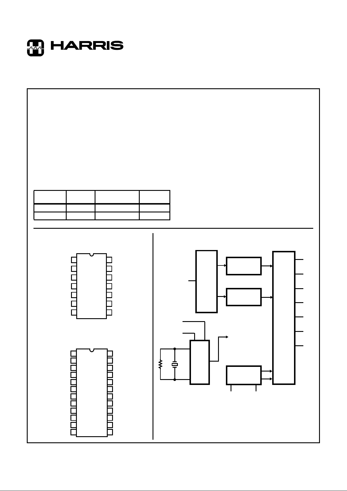
Description
The CD22204 complete dual tone multiple frequency (DTMF)
receiver detects a selectable group of 12 or 16 standard digits. No
front-end pre-filtering is needed. The only externally required components are an inexpensive 3.579545MHz TV ‘‘colorburst’’ crystal
(for frequency reference) and a bias resistor. Extremely high system density is possible through the use of the Alternate Time Base
(ATB) output of a crystal connected CD22204 receiver to drive the
time bases of up to 10 additional receivers. This is a monolithic
integrated circuit fabricated with low power, complementary symmetry CMOS processing. It only requires a single power supply .
The CD22204 employs state-of-the-art ‘‘switched-capacitor’’ filter
technology, resulting in approximately 40 poles of filtering and digital circuitry on the same CMOS chip. The analog input is preprocessed by 60Hz reject and bandsplitting filters and then zero-cross
detected to provide AGC. Eight bandpass filters detect the individual tones. Digital processing is used to measure the tone and
pause durations and provides the correctly coded and timed digital
outputs. The outputs interface directly to standard CMOS circuitry
and are three-state enabled to facilitate bus oriented architectures.
Features
• No Front End Band Splitting Filters Required
• Single Low Tolerance 5V Supply
• Three-State Outputs for Microprocessor Based
Systems
• Detects all 16 Standard DTMF Digits
• Uses Inexpensive 3.579545MHz Crystal
• Excellent Speech Immunity
• Output in 4-Bit Hexadecimal Code
• Excellent Latch-Up Immunity
Ordering Information
PART
NUMBER
TEMP .
RANGE (oC) PACKAGE PKG. NO.
CD22204E 0 to 70 14 Ld PDIP E14.3
CD22204M 0 to 70 24 Ld Plastic SOIC M24.3
January 1997
Pinouts
CD22204 (PDIP)
TOP VIEW
CD22204 (SOIC)
TOP VIEW
D2
D1
EN
V
DD
NC
XEN
ANALOG
D4
D8
DV
ATB
XIN
XOUT
V
SS
1
2
3
4
5
6
7
14
13
12
11
10
9
8
IN
1
2
3
4
5
6
7
8
9
10
11
12
D2
D1
EN
NC
NC
V
DD
NC
NC
NC
NC
XEN
AIN
16
17
18
19
20
21
22
23
24
15
14
13
D4
NC
NC
DV
NC
NC
NC
XOUT
V
SS
D8
ATB
XIN
Functional Diagram
HIGH B/P
FILTERS
LOW B/P
FILTERS
VOLTAGE
REG./REF.
CLOCK
GENERATOR
CHIP
CLOCKS
ATB
XEN
11
6
10
9
48
DETECTORS AND SIGNAL-
PROCESSING CIRCUITS
5
12
2
1
14
13
3
DV
D1
D4
D8
EN
XIN
XOUT
D2
V
SS
V
DD
PREPROCESSOR/
BANDSPLIT FILTER
ANALOG IN
7
NC
NOTE: Pin numbers are for PDIP.
CD22204
5V Low Power Subscriber
DTMF Receiver
CAUTION: These devices are sensitive to electrostatic discharge. Users should follow proper IC Handling Procedures.
Copyright
© Harris Corporation 1997
File Number 1696.3
Page 2
4-2
CD22204
Absolute Maximum Ratings (Note 1) Thermal Information
DC Supply Voltage (VDD) (Referenced to VSS Terminal) . . . . . . . 7V
Power Dissipation
TA = 25oC (Derate above TA = 25oC at 6.25mW/oC. . . . . . . . 65mW
Input Voltage Range
All Inputs Except Analog In. . . . . . . . . . . . . . . (VDD 0.5V) to -0.5V
Analog in Voltage Range . . . . . . . . . . . . . (VDD 0.5V) to (VDD -10V)
DC Current into any Input or Output . . . . . . . . . . . . . . . . . . . . . .±20mA
Maximum Junction Temperature . . . . . . . . . . . . . . . . . . . . . . . 175oC
Maximum Junction Temperature (Plastic) . . . . . . . . . . . . . . . . 150oC
Maximum Storage Temperature Range . . . . . . . . . .-65oC to 150oC
Maximum Lead Temperature (Soldering 10s). . . . . . . . . . . . . 300oC
Operating Conditions
Temperature Range . . . . . . . . . . . . . . . . . . . . . . . . . . . 0oC to 70oC
CAUTION: Stresses above those listed in “Absolute Maximum Ratings” may cause permanent damage to the device. This is a stress only rating and operation
of the device at these or any other conditions above those indicated in the operational sections of this specification is not implied.
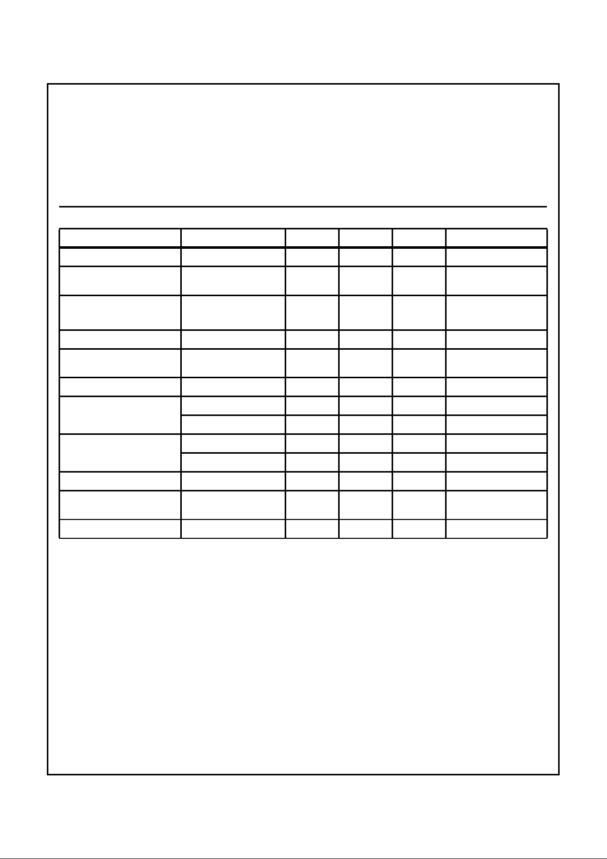
Electrical Specifications 0
o
C ≤ TA≤ 70oC, VDD = 5V ±10%
PARAMETER TEST CONDITIONS MIN TYP MAX UNITS
Frequency Detect Bandwidth ±(1.5 + 2Hz) ±2.3 ±3.5 % of f
O
Amplitude for Detection Each Tone -32
(Note 3)
- -2 dBm Referenced to 600Ω
Minimum Acceptable Twist -8 - +4 dB
60Hz Tolerance - - 0.8 V
RMS
Dial Tone Tolerance “Precise” Dial Tone - - 0 dB Referenced to Lower
Amplitude Tone
Talk Off MITEL Tape #CM7291 - 2 - Hits
Digital Outputs (except XOUT) “0” Level, 400µA Load 0 - 0.5 V
“1” Level, 200µA Load VDD -0.5 - V
DD
V
Digital Inputs “0” Level 0 - 0.3V
DD
V
“1” Level 0.7V
DD
-VDDV
Supply Current TA = 25oC - 10 20 mA
Noise Tolerance MITEL Tape #CM7291
(Note 2)
- - -12 dB Referenced to Lowest
Amplitude Tone
Input Impedance VDD≥ VIN≥ (VDD -10) 100kΩ//15pF 300kΩ -
NOTES:
1. Unused inputs must be connected to VDD or VSS as appropriate.
2. Bandwidth limited (3kHz) Gaussian noise.
3. Lower minimum available, please contact sales office.
(-32dBm = 19.45mV
RMS
, -2dBm = 0.615mV
RMS
)
Tw ist
High Tone
Low To ne
--------------------------- -=
Page 3

4-3
CD22204
Functional Block Diagram
÷8
60Hz
REJECT
CLOCK
GENERATOR
CHIP CLOCKS
PRE EMP
POWER REGULATOR
4 8
V
DD
V
SS
VOLTAGE
REF
697
770
852
941
1209
1336
1477
1633
BAND
SPLIT
FILTERS
ZERO
CROSSING
DETECTORS
BANDPASS
FILTERS
AMPLITUDE
DETECTORS
OUTPUT
DECODER
OUTPUT
REGISTER
TIMING
CIRCUITRY
DATA STROBE
12
2
1
14
13
3
DATA CLEAR
DV
D1
D2
D4
D8
EN
ANALOG
IN
PREPROCESSOR
7
BS1
BS2
10
9
11
6
ATB
XEN
XIN
XOUT
1M
NOTE: Pin numbers are for plastic DIP.
System Functions
Analog In
The Analog In pin accepts the analog input. It is internally
biased so that the input signal may be either AC or DC coupled, as long as it does not exceed the positive supply voltage. Proper input coupling is illustrated below.
FIGURE 1. ANALOG IN
7
V
SS
V
DD
10pF
>100kΩ
(ON CHIP)
270kΩ
33kΩ
ANALOG
IN
1500pF
OPTIONAL
HIGH FREQUENCY
NOISE FILTER
(f
C
= 3.9kHz)
AUDIO
INPUT
(+4dBm OR
1.22V
RMS
0.01µF
CD22204E
MAXIMUM)
The CD22204 is designed to accept sinusoidal input waveforms, but will operate satisfactorily with any input that has
the correct fundamental frequency with harmonics that are
at least 20dB below the fundamental.
Crystal Oscillator
The CD22204 contains an on-board inverter with sufficient
gain to provide oscillation when connected to a low cost television “color-burst” (3.579545MHz) crystal. The crystal oscillator is enabled by tying XEN high. The crystal is connected
between XIN and XOUT. A 1MΩ resistor is also connected
between these pins in this mode. ATB is a clock frequency
output. Other CD22204 devices may use the same frequency reference by tying their ATB pins to the ATB output of
a crystal connected device. XIN and XEN of the auxiliary
devices must then be tied high and low, respectively. Up to
ten devices may be run from a single crystal connected
CD22204 as shown in Figure 2.
Page 4

4-4
CD22204
FIGURE 2. CRYSTAL OSCILLATOR
Outputs D1, D2, D4, D8 and EN
Outputs D1, D2, D4, D8 are CMOS push-pull when enabled
(EN high) and open circuited (high impedance) when disabled by pulling EN low. These digital outputs provide the
hexadecimal code corresponding to the detected digit. The
digital outputs become valid after a tone pair has been
detected and they are then cleared when a valid pause is
timed. The table below describes the hexadecimal codes.
DV
DV signals a detection by going high after a valid tone pair is
sensed and decoded at the output pins D1, D2, D4, and D8.
DV remains high until a valid pause occurs.
N/C Pin
This pin has no internal connection and should be left floating.
DTMF Dialing Matrix
Digital Inputs and Outputs
All digital inputs and outputs of the DTMF receivers are represented by the schematic below. Only the “analog in” pin is
different, and is described above. Care must be exercised
not to exceed the voltage or current ratings on these pins as
listed in the “maximum ratings” section.
FIGURE 3. DIGITAL INPUTS AND OUTPUTS
Input Filter
The CD22204 will tolerate total input noise of a maximum
of 12dB below the lowest amplitude tone. For most
telephone applications, the combination of the high
frequency attenuation of the telephone line and internal
band limiting make special circuitry at the input to these
receivers unnecessary. However, noise near the 56kHz
internal sampling frequency will be aliased (folded back)
into the audio spectrum, so if excessive noise is present
above 28kHz, the simple RC filter shown below may be
used to band limit the incoming signal. The cut off
frequency is 3.9kHz.
FIGURE 4. FILTER FOR USE IN EXTREME HIGH FREQUENCY
INPUT NOISE ENVIRONMENT
TABLE 1. OUTPUT CODES
DIGIT D8 D4 D2 D1
10001
20010
30011
40100
50101
60110
70111
81000
91001
01010
*1011
#1100
A1101
B1110
C1111
D0000
XEN
XEN
CD22204
10 9
6
11
ATB
XIN
3.579545MHz
V
DD
XOUT
1M
10
11 6
XIN CONNECTED TO V
DD
UP TO 10 DEVICES
CD22204
COL 0
1209Hz
COL 1
1336Hz
COL 2
1477Hz
COL 3
1633Hz
ROW 0
697Hz
ROW 1
770Hz
ROW 2
852Hz
ROW 3
941Hz
NOTE: Column 3 is for special applications and is not normally used
in telephone dialing.
1
2 3 A
4 5 6 B
7 8 9 C
* 0 # D
V
DD
V
SS
CMOS
DIGITAL
CIRCUITRY
DIGITAL
OUTPUT
DIGITAL
INPUT
CD22204
33kΩ
0.0015µF
270kΩ
ANALOG
IN
NOISY
SIGNAL
Page 5

4-5
All Harris Semiconductor products are manufactured, assembled and tested under ISO9000 quality systems certification.
Harris Semiconductor products are sold by description only. Harris Semiconductor reserves the right to make changes in circuit design and/or specifications at
any time without notice. Accordingly, the reader is cautioned to verify that data sheets are current before placing orders. Information furnished by Harris is
believed to be accurate and reliable. However, no responsibility is assumed by Harris or its subsidiaries for its use; nor for any infringements of patents or other
rights of third parties which may result from its use. No license is granted by implication or otherwise under any patent or patent rights of Harris or its subsidiaries.
Sales Office Headquarters
For general information regarding Harris Semiconductor and its products, call 1-800-4-HARRIS
NORTH AMERICA
Harris Semiconductor
P. O. Box 883, Mail Stop 53-210
Melbourne, FL 32902
TEL: 1-800-442-7747
(407) 729-4984
FAX: (407) 729-5321
EUROPE
Harris Semiconductor
Mercure Center
100, Rue de la Fusee
1130 Brussels, Belgium
TEL: (32) 2.724.2111
FAX: (32) 2.724.22.05
ASIA
Harris Semiconductor PTE Ltd.
No. 1 Tannery Road
Cencon 1, #09-01
Singapore 1334
TEL: (65) 748-4200
FAX: (65) 748-0400
SEMICONDUCTOR
CD22204
Noise will also be reduced by placing a grounded trace
around XIN and XOUT pins on the circuit board layout when
using a crystal. It is important to note that XOUT is not
intended to drive an additional device. XIN may be driven
externally; in this case, leave XOUT floating.
Timing Waveforms
FIGURE 5.
t
ON
t
OFF
PAUSE
ANALOG
INPUT
D1, D2
D4, D8
TONE BURST 1
TONE BURST 2
t
D
t
R
t
SU
t
H
DV
PARAMETER SYMBOL MIN TYP MAX UNITS
Tone Time
For Detection t
ON
40 - - ms
For Rejection t
ON
- - 20 ms
Pause Time
For Detection t
OFF
40 - - ms
For Rejection t
OFF
- - 20 ms
Detect Time t
D
25 - 46 ms
Release Time t
R
35 50 ms
Data Setup Time t
SU
7--µs
Data Hold Time t
H
4.2 - 5 ms
Output Enable Time
CL = 50pF, RL = 1kΩ
- - 200 300 ns
Output Disable Time
CL = 35pF, RL = 500Ω
- - 150 200 ns
Output Rise Time
CL = 50pF
- - 200 300 ns
Output Fall Time
CL = 50pF
- - 160 250 ns
 Loading...