

Page 1
DTMF Receivers/Generators
CD22202, CD22203
January 1997
Features
• Central Office Quality
• No Front End Band Splitting Filters Required
• Single, Low Tolerance, 5V Supply
• Detects Either 12 or 16 Standard DTMF Digits
• Uses Inexpensive 3.579545MHz Crystal for Reference
• Excellent Speech Immunity
• Output in Either 4-Bit Hexadecimal Code or Binary
Coded 2-of-8
• Synchronous or Handshake Interface
• Three-State Outputs
• Excellent Latch-Up Immunity
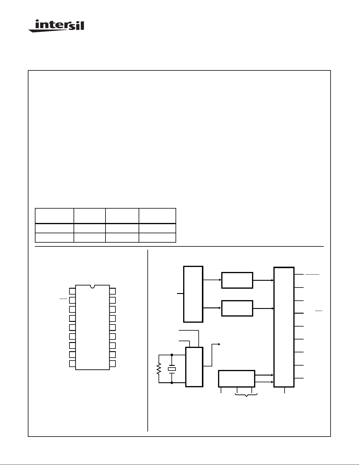
Ordering Information
PART
NUMBER
CD22202E 0 to 70 18 Ld PDIP E18.3
CD22203E 0 to 70 18 Ld PDIP E18.3
TEMP .
RANGE (oC) PACKAGE PKG. NO.
5V Low Power DTMF Receiver
Description
The CD22202 and CD22203 complete dual-tone multiple
frequency (DTMF) receivers detect a selectable group of 12
or 16 standard digits. No front-end pre-filtering is needed.
The only externally required components are an inexpensive
3.579545MHz TV “colorburst’’ crystal (for frequency reference) and a bias resistor. Extremely high system density is
possible through the use of the clock output of a crystal connected CD22202/CD22203 receiver to drive the time bases
of additional receivers. This is a monolithic integrated circuit
fabricated with low-power, complementary symmetry CMOS
processing. It only requires a single low tolerance power
supply.
The CD22202 and CD22203 employ state-of-the-art circuit
technology to combine the digital and analog functions on
the same CMOS chip using a standard digital semiconductor
process. The analog input is preprocessed by 60Hz reject
and band splitting filters and then hard limited to provide
AGC. Eight Bandpass filters detect the individual tones. The
digital post processor times the tone durations and provides
the correctly coded digital outputs. Outputs interface directly
to standard CMOS circuitry and are three-state enabled to
facilitate bus oriented architectures.
Pinout
HEX/B28
IN1633
ED (203 ONLY),
NC (202)
XEN
ANALOG IN
CD22202, CD22203
(PDIP)
TOP VIEW
D1
1
2
3
EN
4
5
V
DD
6
7
V
SS
8
9
18
17
16
15
14
13
12
11
10
D2
D4
D8
CLRDV
DV
ATB
XIN
XOUT
V
SS
Functional Diagram
ATB
XEN
XIN
XOUT
9
13
8
12
11
PREPROCESSOR/
BANDSPLIT FILTER
CLOCK
GENERATOR
ANALOG IN
LOW B/P
FILTERS
HIGH B/P
FILTERS
CHIP
CLOCKS
VOLTAGE
REG./REF.
5107
V
DD
V
SS
6
ED-203
NC-202
15
CLRDV
14
DV
2
HEX/B28
1
D1
18
D2
17
PROCESSING CIRCUITS
DETECTORS AND SIGNAL-
4
INI633
D4
16
D8
3
EN
CAUTION: These devices are sensitive to electrostatic discharge; follow proper IC Handling Procedures.
http://www.intersil.com or 407-727-9207
| Copyright © Intersil Corporation 1999
4-245
File Number 1695.3
Page 2
CD22202, CD22203
Absolute Maximum Ratings Thermal Information
DC Supply Voltage (VDD)(Referenced to VSS Terminal). . . . . . . . 7V
Power Dissipation
TA = 25oC (Derate above TA = 25oC at 6.25mW/oC. . . . . . . . 65mW
Input Voltage Range
All Inputs Except Analog In. . . . . . . . . . . . . . (VDD +0.5V) to -0.5V
Analog in Voltage Range . . . . . . . . . . . . (VDD +0.5V) to (VDD -10V)
DC Current into any Input or Output . . . . . . . . . . . . . . . . . . . . . .±20mA
NOTE: Unused inputs must be connected to VDD or VSS as appropriate.
CAUTION: Stresses above those listed in “Absolute Maximum Ratings” may cause permanent damage to the device. This is a stress only rating and operation
of the device at these or any other conditions above those indicated in the operational sections of this specification is not implied.
Maximum Junction Temperature. . . . . . . . . . . . . . . . . . . . . . . 175oC
Maximum Junction Temperature (Plastic). . . . . . . . . . . . . . . . 150oC
Maximum Storage Temperature Range . . . . . . . . . . -65oC to 150oC
Maximum Lead Temperature (Soldering 10s). . . . . . . . . . . . . 300oC
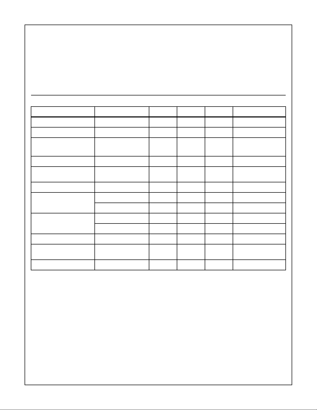
Operating Conditions
Temperature Range . . . . . . . . . . . . . . . . . . . . . . . . . . . 0oC to 70oC
Electrical Specifications 0
o
C ≤ TA≤ +70oC, VDD = 5V ±10%
PARAMETER TEST CONDITIONS MIN TYP MAX UNITS
Frequency Detect Bandwidth ±(1.5 + 2Hz) ±2.3 ±3.5 % of f
O
Amplitude for Detection Each Tone -32 - -2 dBm Referenced to 600Ω
Minimum Acceptable Twist -10 - +10 dB
Tw ist
60Hz Tolerance - - 0.8 V
High Tone
--------------------------- -=
Low Tone
RMS
Dial Tone Tolerance “Precise” Dial Tone - - 0 dB Referenced to Lower
Amplitude Tone
Talk Off MITEL Tape #CM7291 - 2 - Hits
Digital Outputs (except XOUT) “0” Level, 400µA Load 0 - 0.5 V
“1” Level, 200µA Load VDD -0.5 - V
Digital Inputs “0” Level 0 - 0.3V
“1” Level 0.7V
DD
-VDDV
DD
DD
V
V
Supply Current TA = +25oC - 10 16 mA
Noise Tolerance MITEL Tape #CM7291
(Note 1)
- - -12 dB Referenced to Lowest
Amplitude Tone
Input Impedance VDD≥ VIN≥ (VDD -10) 100kΩ//15pF 300kΩ -
NOTE:
1. Bandwidth limited (3kHz) Gaussian noise.
4-246
Page 3

Functional Block Diagram
CD22202, CD22203
1MΩ
ANALOG
ATB
XEN
XOUT
IN
13
12
XIN
11
DV
F.F
OUTPUT
CD22202
CD22203
CLR
EARLY
DETECT
OUTPUT
6
CLRDV
15
DV
14
H/B28
2
1
D1
18
D2
17
D4
16
D8
3
EN
BANDPASS
FILTERS
BAND
PREPROCESSOR
9
8
60Hz
REJECT
PRE EMP
÷8
V
SPLIT
FILTERS
BS1
BS2
GENERATOR
POWER REGULATOR
5 10 7
V
DD
SS
CROSSING
DETECTORS
CLOCK
V
SS
ZERO
697
770
852
941
1209
1336
1477
1633
CHIP CLOCKS
AMPLITUDE
DETECTORS
VOLTAGE
REF
DATA STROBE
OUTPUT
DECODER
IN1633
TIMING
CIRCUITRY
DV
STROBE
DATA CLEAR
4
REGISTER
NOTE: Pin 6: Early detect output on CD22203 only.
System Functions
Analog In
The Analog In pin accepts the analog input. It is internally
biased so that the input signal may be either AC or DC coupled, as long as it does not exceed the positive supply voltage. Proper input coupling is illustrated below.
9
IN
CD22202, CD22203
V
DD
(ON CHIP)
>100kΩ
V
SS
10pF
AUDIO
INPUT
(+4dBm
MAXIMUM)
1500pF
0.01µF
270kΩ
ANALOG
33kΩ
OPTIONAL
HIGH FREQUENCY
NOISE FILTER
= 3.9kHz)
(f
C
The CD22202 and CD22203 are designed to accept sinusoidal input waveforms, but will operate satisfactorily with any
input that has the correct fundamental frequency with harmonics that are at least 20dB below the fundamental.
Crystal Oscillator
The CD22202 and CD22203 contain an on-board inverter
with sufficient gain to provide oscillation when connected to
a low cost television “color-burst” (3.579545MHz) crystal.
The crystal oscillator is enabled by tying XEN high. The crystal is connected between XIN and XOUT. A 1MΩ resistor is
also connected between these pins in this mode. ATB is a
clock frequency output. Other CD22202 and CD22203
devices may use the same frequency ref erence b y tying their
ATB pins to the ATB output of a crystal connected device.
XIN and XEN of the auxiliary devices must then be tied high
and low, respectively. Up to ten devices may be run from a
single crystal connected CD22202 and CD22203 as shown
in Figure 2.
FIGURE 1. ANALOG IN
4-247
Page 4

CD22202, CD22203
3.579545MHz
1M
XIN
12 11
ATB
UP TO 10 DEVICES
FIGURE 2. CRYSTAL OSCILLATOR
CD22202/22203
13
XIN CONNECTED TO V
12
CD22202/22203
13 8
XOUT
DD
V
DD
8
XEN
XEN
HEX/B28
This pin selects the format of the digital output code. When
HEX/
B28 is tied high, the output is hexadecimal. When tied
low, the output is binary coded 2-of-8. The following table
describes the two output codes.
TABLE 1. OUTPUT CODES
HEXADECIMAL BINARY CODED 2-OF-8
DIGIT
D8 D4 D2 D1 D8 D4 D2 D1
1 00010000
2 00100001
3 00110010
4 01000100
5 01010101
6 01100110
7 01111000
8 10001001
9 10011010
0 10101101
* 10111100
# 11001110
A 11010011
B 11100111
C 11111011
D 00001111
DV remains high until a valid pause occurs or CLRDV is
raised high, whichever is sooner. This handshake can save
microprocessor time.
DTMF Dialing Matrix
COL 0
1209Hz
ROW 0
697Hz
ROW 1
770Hz
ROW 2
852Hz
ROW 3
941Hz
NOTE: Column 3 is for special applications and is not normally used
in telephone dialing.
1
4 5 6 B
7 8 9 C
* 0 # D
COL 1
1336Hz
2 3 A
COL 2
1477Hz
COL 3
1633Hz
IN1633
When tied high, this pin inhibits detection of tone pairs containing the 1633Hz component. For detection of all 16 standard digits, IN1633 must be tied low.
N/C Pin
This pin has no internal connection and should be left floating.
Digital Inputs and Outputs
All digital inputs and outputs of the DTMF receivers are represented by the schematic below. Only the “analog in” pin is
different, and is described above. Care must be exercised
not to exceed the voltage or current ratings on these pins as
listed in the “maximum ratings” section.
V
DD
DIGITAL
INPUT
FIGURE 3. DIGITAL INPUTS AND OUTPUTS
CMOS
DIGITAL
CIRCUITRY
V
SS
DIGITAL
OUTPUT
ED
This pin, on the CD22203 only, indicates the presence of frequencies which are likely to be DTMF digits, but have not yet
been verified by a DV signal. It is comparable to a “buttondown” output, and it is useful as an EARLY DETECT signal to
interrupt a microprocessor for digit storage and validation.
DV and CLRDV
DV signals a detection by going high after a valid tone pair is
sensed and decoded at the output pins D1, D2, D4, and D8.
Input Filter
The CD22202 and CD22203 will tolerate total input noise of
a maximum of 12dB below the lowest amplitude tone. For
most telephone applications, the combination of the high
frequency attenuation of the telephone line and internal
band limiting make special circuitry at the input to these
receivers unnecessary. However, noise near the 56kHz
internal sampling frequency will be aliased (folded back)
into the audio spectrum, so if excessive noise is present
4-248
Page 5

CD22202, CD22203
above 28kHz, the simple RC filter shown below may be
used to band limit the incoming signal. The cut off
frequency is 3.9kHz.
NOISY
SIGNAL
270kΩ
0.0015µF
FIGURE 4. FILTER FOR USE IN EXTREME HIGH FREQUENCY
INPUT NOISE ENVIRONMENT
ANALOG
IN
33kΩ
CD22202
CD22203
Noise will also be reduced by placing a grounded trace
around XIN and XOUT pins on the circuit board layout when
using a crystal. It is important to note that XOUT is not
intended to drive an additional device. XIN may be driven
externally; in this case, leave XOUT floating.
Timing Waveforms
TONE BURST 1
ANALOG
INPUT
D1, D2
D4, D8
t
ON
t
D
t
SU
t
OFF
PAUSE
t
R
TONE BURST 2
t
H
t
CL
PARAMETER SYMBOL MIN TYP MAX UNITS
Tone Time
For Detection t
For Rejection t
ON
ON
40 - - ms
- - 20 ms
Pause Time
For Detection t
For Rejection t
Detect Time t
Release Time t
Data Setup Time t
Data Hold Time t
DV Clear Time t
CLRDV Pulse Width t
ED Detect Time t
ED Release Time t
Output Enable Time
OFF
OFF
D
R
SU
H
CL
PW
ED
ER
- - 200 300 ns
40 - - ms
- - 20 ms
25 - 46 ms
35 50 ms
7--µs
4.2 - 5 ms
- 160 250 ns
200 - - ns
7 - 22 ms
2 - 18 ms
CL = 50pF, RL = 1kΩ
Output Disable Time
- - 150 200 ns
CL = 35pF, RL = 500Ω
Output Rise Time
- - 200 300 ns
CL = 50pF
Output Fall Time
- - 160 250 ns
CL = 50pF
DV
CLRDV
t
ED
ED
(NOTE)
t
ER
NOTE: Early Detect output is available only on the CD22203.
FIGURE 5.
Guard Time
t
PW
Whenever the DTMF receiver is continually monitoring a
voice channel containing distorted or musical voices or
tones, additional guard time may be added in order to
prevent false decoding. This may be done in software by
verifying that both ED and D V are present simultaneously for
about 55ms. An appropriate guard time should be selected
to balance the fastest expected dialing speed against the
rejection of distorted or musical voices or tones (most
autodialers operate in the 65ms to 75ms range although a
few generate 50ms tones). A hardware guard time circuit is
shown in Figure 6. R
amplitude as low as practical, while R
and R4 should keep the voice
3
and R5 adjust
2
detection speed.
4-249
Page 6

+5V
10µF
R
2
≈240K
(55ms)
IN4148
C
2
0.15µF
R
5
1.8M
R
6
100K
ENABLE
1
/3 CD74HC04
INPUT
(BUFFERS OPTIONAL)
DV
OUT
CD22202, CD22203
D1
1
HEX/B28
ANALOG IN
R
4
33K
IN1633
EN
V
DD
ED
V
SS
XEN
2
3
4
5
6
7
8
9
18
17
16
15
14
13
12
11
10
R
3
≈390K
D2
D4
D8
CLRDV
DV
ATB
XIN
XOUT
V
SS
C
1
4700pF
3.58
MHz
R
1
1M
D8
D4 D2 D1
HEX DATA OUT
AUDIO
IN
FIGURE 6. CD22203 DTMF RECEIVER WITH GUARD TIME CIRCUIT TO PROVIDE EXCEPTIONAL TALK-OFF PERFORMANCE
Operating and Handling Considerations
Handling
All inputs and outputs of CMOS devices have a network for
electrostatic protection during handling. Recommended handling practices for CMOS devices are described in
ICAN-6525 “Guide to Better Handling and Operation of
CMOS Integrated Circuits”.
Operating
Operating Voltage
During operation near the maximum supply voltage limit,
care should be taken to avoid or suppress power supply
turn-on and turnoff transients, power supply ripple, or ground
noise; any of these conditions must not cause V
exceed the absolute maximum rating.
All Intersil semiconductor products are manufactured, assembled and tested under ISO9000 quality systems certification.
Intersil products are sold by description only. Intersil Corporation reserves the right to make changes in circuit design and/or specifications at any time without
notice. Accordingly, the reader is cautioned to verify that data sheets are current before placing orders. Information furnished by Intersil is believed to be accurate
and reliable. However, no responsibility is assumed by Intersil or its subsidiaries for its use; nor for any infringements of patents or other rights of third parties which
may result from its use. No license is granted by implication or otherwise under an y patent or patent rights of Intersil or its subsidiaries.
For information regarding Intersil Corporation and its products, see web site http://www.inter sil.com
- VSS to
DD
Input Signals
To prevent damage to the input protection circuit, input signals should never be greater than V
nor less than VSS.
DD
Input currents must not exceed 20mA even when the power
supply is off.
Unused Inputs
A connection must be provided at every input terminal. All
unused input terminals must be connected to either V
V
, whichever is appropriate.
SS
DD
or
Output Short Circuits
Shorting of outputs to V
or VSS may damage CMOS
DD
devices by exceeding the maximum device dissipation.
4-250
 Loading...