

Page 1

Product
Folder
Order
Now
Technical
Documents
Tools &
Software
Support &
Community
Reference
Design
CC2650MODA SimpleLink™ Bluetooth®low energy Wireless MCU Module
1 Device Overview
1.1 Features
1
• Microcontroller
– Powerful ARM®Cortex®-M3
– EEMBC CoreMark®Score: 142
– Up to 48-MHz Clock Speed
– 128KB of In-System Programmable Flash
– 8KB of SRAM for Cache
– 20KB of Ultra-Low-Leakage SRAM
– 2-Pin cJTAG and JTAG Debugging
– Supports Over-The-Air (OTA) Upgrade
• Ultra-Low-Power Sensor Controller
– Can Run Autonomous From the Rest of the
System
– 16-Bit Architecture
– 2KB of Ultra-Low-Leakage SRAM for
Code and Data
• Efficient Code Size Architecture, Placing Drivers,
Bluetooth®low energy Controller, IEEE®802.15.4
Medium Access Control (MAC), and Bootloader in
ROM
• Integrated Antenna
• Peripherals
– All Digital Peripheral Pins Can Be Routed to
Any GPIO
– Four General-Purpose Timer Modules
(8 × 16-Bit or 4 × 32-Bit Timer, PWM Each)
– 12-Bit ADC, 200-ksamples/s, 8-Channel
Analog MUX
– Continuous Time Comparator
– Ultra-Low-Power Analog Comparator
– Programmable Current Source
– UART
– 2 × SSI (SPI, MICROWIRE, TI)
– I2C
– I2S
– Real-Time Clock (RTC)
– AES-128 Security Module
– True Random Number Generator (TRNG)
– 15 GPIOs
– Support for Eight Capacitive Sensing Buttons
– Integrated Temperature Sensor
• External System
– On-Chip Internal DC-DC Converter
– No External Components Needed, Only Supply
Voltage
CC2650MODA
SWRS187D –AUGUST 2016–REVISED JULY 2019
• Low Power
– Wide Supply Voltage Range
– Operation from 1.8 to 3.8 V
– Active-Mode RX: 6.2 mA
– Active-Mode TX at 0 dBm: 6.8 mA
– Active-Mode TX at +5 dBm: 9.4 mA
– Active-Mode MCU: 61 µA/MHz
– Active-Mode MCU: 48.5 CoreMark/mA
– Active-Mode Sensor Controller:
0.4 mA + 8.2 µA/MHz
– Standby: 1 µA (RTC Running and RAM/CPU
Retention)
– Shutdown: 100 nA (Wake Up on External
Events)
• RF Section
– 2.4-GHz RF Transceiver Compatible With
Bluetooth low energy (BLE) 5.1 Specification
and IEEE 802.15.4 PHY and MAC
– CC2650MODA RF-PHY Qualified (QDID:
88415)
– Excellent Receiver Sensitivity (–97 dBm for
Bluetooth low energy and –100 dBm for
802.15.4), Selectivity, and Blocking
Performance
– Programmable Output Power up to +5 dBm
– Pre-certified for Compliance With Worldwide
Radio Frequency Regulations
– ETSI RED (Europe)
– IC (Canada)
– FCC (USA)
– ARIB STD-T66 (Japan)
– JATE (Japan)
• Tools and Development Environment
– Full-Feature and Low-Cost Development Kits
– Multiple Reference Designs for Different RF
Configurations
– Packet Sniffer PC Software
– Sensor Controller Studio
– SmartRF™ Studio
– SmartRF Flash Programmer 2
– IAR Embedded Workbench®for ARM
– Code Composer Studio™
1
An IMPORTANT NOTICE at the end of this data sheet addresses availability, warranty, changes, use in safety-critical applications,
intellectual property matters and other important disclaimers. PRODUCTION DATA.
Page 2

CC2650MODA
SWRS187D –AUGUST 2016–REVISED JULY 2019
1.2 Applications
• Building Automation
• Medical and Health
• Appliances
• Industrial
• Consumer Electronics
1.3 Description
The SimpleLink™ CC2650MODA device is a wireless microcontroller (MCU) module that targets
Bluetooth®low energy applications. The CC2650MODA device can also run ZigBee®and 6LoWPAN and
ZigBee RF4CE™ remote control applications.
The module is based on the SimpleLink CC2650 wireless MCU, a member of the CC26xx family of cost-
effective, ultra-low-power, 2.4-GHz RF devices. Very-low active RF and MCU current and low-power mode
current consumption provide excellent battery lifetime and allow for operation on small coin-cell batteries
and in energy-harvesting applications.
The CC2650MODA module contains a 32-bit ARM Cortex-M3 processor that runs at 48 MHz as the main
processor and a rich peripheral feature set that includes a unique ultra-low-power sensor controller. This
sensor controller is good for interfacing with external sensors or for collecting analog and digital data
autonomously while the rest of the system is in sleep mode. Thus, the CC2650MODA device is good for
applications within a wide range of products including industrial, consumer electronics, and medical
devices.
www.ti.com
• Proximity Tags
• Alarm and Security
• Remote Controls
• Wireless Sensor Networks
The CC2650MODA module is pre-certified for operation under the regulations of the FCC, IC, ETSI, and
ARIB. These certifications save significant cost and effort for customers when integrating the module into
their products.
The Bluetooth low energy controller and the IEEE 802.15.4 MAC are embedded in the ROM and are partly
running on a separate ARM®Cortex®-M0 processor. This architecture improves overall system
performance and power consumption and makes more flash memory available.
The Bluetooth low energy software stack (BLE-Stack) and the ZigBee software stack ( Z-Stack™) are
available free of charge.
Device Information
PART NUMBER PACKAGE BODY SIZE
CC2650MODAMOH MOH (Module) 16.90 mm × 11.00 mm
(1) For more information, see Section 10.
(1)
2
Device Overview Copyright © 2016–2019, Texas Instruments Incorporated
Submit Documentation Feedback
Product Folder Links: CC2650MODA
Page 3
Main CPU
128-KB
Flash
Sensor Controller
cJTAG
20-KB
SRAM
ROM
ARM
Cortex-M3
DC-DC Converter
RF core
ARM
Cortex-M0
DSP Modem
4-KB
SRAM
ROM
Sensor Controller Engine
2× Analog Comparators
12-bit ADC, 200 ks/s
Constant Current Source
SPI / I2C Digital Sensor IF
2-KB SRAM
Time-to-Digital Converter
General Peripherals / Modules
4× 32-bit Timers
2× SSI (SPI, µWire, TI)
Watchdog Timer
Temp. / Batt. Monitor
RTC
I2C
UART
I2S
15 GPIOs
AES
32 ch. µDMA
ADC
ADC
Digital PLL
SimpleLink CC2650MODA Wireless MCU Module
TRNG
8-KB
Cache
24-MHz Crystal
Oscillator
32.768-kHz
Crystal
Oscillator
RF Balun
Copyright © 2017, Texas Instruments Incorporated
www.ti.com
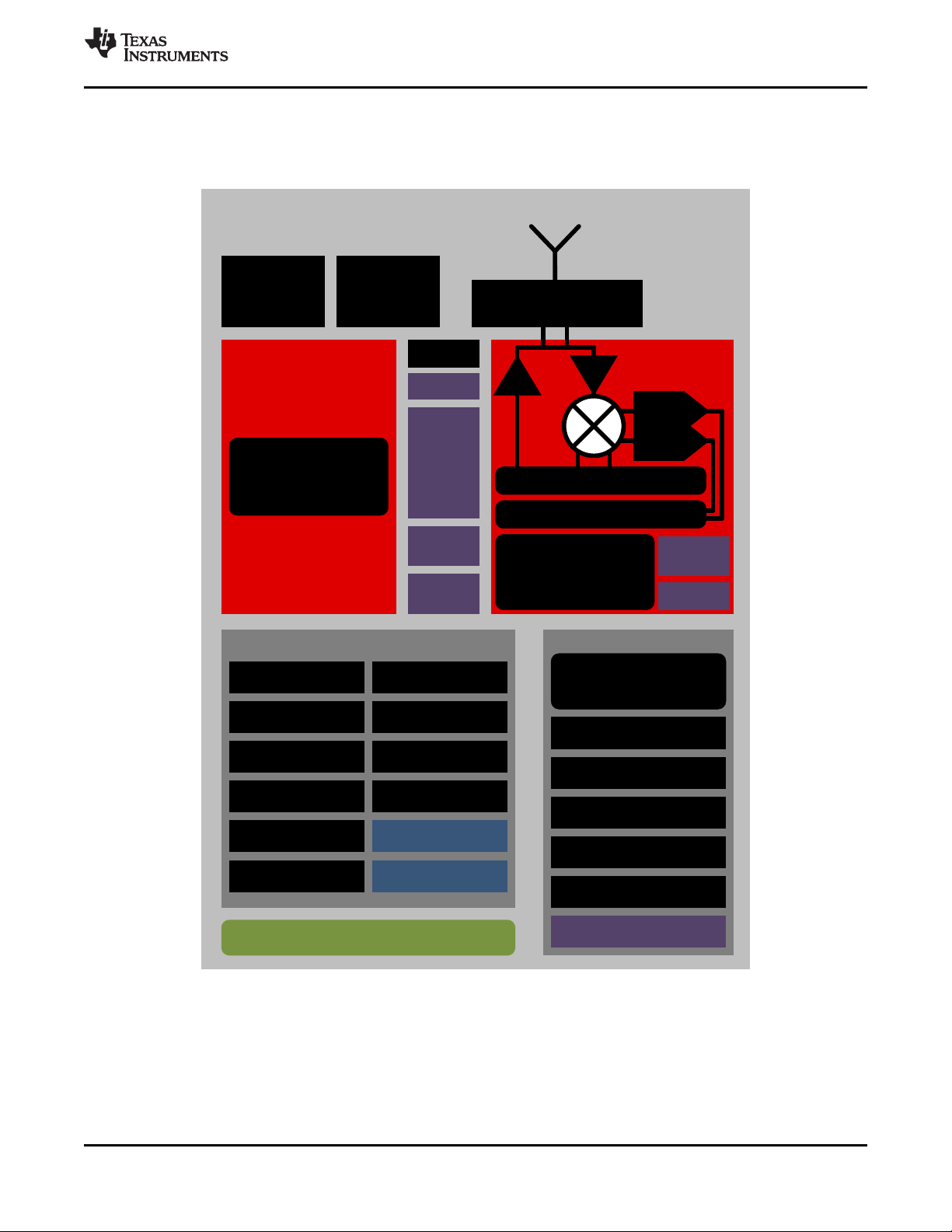
1.4 Functional Block Diagram
Figure 1-1 is a block diagram for the CC2650MODA device.
CC2650MODA
SWRS187D –AUGUST 2016–REVISED JULY 2019
Figure 1-1. CC2650MODA Block Diagram
Submit Documentation Feedback
Product Folder Links: CC2650MODA
Device OverviewCopyright © 2016–2019, Texas Instruments Incorporated
3
Page 4

CC2650MODA
SWRS187D –AUGUST 2016–REVISED JULY 2019
www.ti.com
Table of Contents
1 Device Overview ......................................... 1
1.1 Features .............................................. 1
1.2 Applications........................................... 2
1.3 Description............................................ 2
1.4 Functional Block Diagram ............................ 3
2 Revision History ......................................... 5
3 Device Comparison ..................................... 6
3.1 Related Products ..................................... 6
4 Terminal Configuration and Functions.............. 7
4.1 Module Pin Diagram.................................. 7
4.2 Pin Functions ......................................... 8
5 Specifications ............................................ 9
5.1 Absolute Maximum Ratings .......................... 9
5.2 ESD Ratings.......................................... 9
5.3 Recommended Operating Conditions ................ 9
5.4 Power Consumption Summary...................... 10
5.5 General Characteristics ............................. 10
5.6 Antenna ............................................. 11
5.7 1-Mbps GFSK (Bluetooth low energy) – RX ........ 11
5.8 1-Mbps GFSK (Bluetooth low energy) – TX ........ 12
5.9 IEEE 802.15.4 (Offset Q-PSK DSSS, 250 kbps) –
RX ................................................... 12
5.10 IEEE 802.15.4 (Offset Q-PSK DSSS, 250 kbps) –
TX ................................................... 13
5.11 24-MHz Crystal Oscillator (XOSC_HF) ............. 13
5.12 32.768-kHz Crystal Oscillator (XOSC_LF).......... 13
5.13 48-MHz RC Oscillator (RCOSC_HF) ............... 13
5.14 32-kHz RC Oscillator (RCOSC_LF)................. 13
5.15 ADC Characteristics................................. 14
5.16 Temperature Sensor ................................ 15
5.17 Battery Monitor...................................... 15
5.18 Continuous Time Comparator....................... 15
5.19 Low-Power Clocked Comparator ................... 15
5.20 Programmable Current Source ..................... 16
5.21 DC Characteristics .................................. 16
5.22 Thermal Resistance Characteristics for MOH
Package ............................................. 17
5.23 Timing Requirements ............................... 17
5.24 Switching Characteristics ........................... 17
5.25 Typical Characteristics .............................. 20
6 Detailed Description ................................... 24
6.1 Overview ............................................ 24
6.2 Functional Block Diagram........................... 24
6.3 Main CPU ........................................... 25
6.4 RF Core ............................................. 25
6.5 Sensor Controller ................................... 26
6.6 Memory.............................................. 27
6.7 Debug ............................................... 27
6.8 Power Management................................. 28
6.9 Clock Systems ...................................... 29
6.10 General Peripherals and Modules .................. 29
6.11 System Architecture................................. 30
6.12 Certification.......................................... 30
6.13 End Product Labeling ............................... 32
6.14 Manual Information to the End User ................ 32
6.15 Module Marking ..................................... 33
7 Application, Implementation, and Layout ......... 34
7.1 Application Information.............................. 34
7.2 Layout ............................................... 35
8 Environmental Requirements and
Specifications........................................... 36
8.1 PCB Bending........................................ 36
8.2 Handling Environment .............................. 36
8.3 Storage Condition ................................... 36
8.4 Baking Conditions................................... 36
8.5 Soldering and Reflow Condition .................... 37
9 Device and Documentation Support ............... 38
9.1 Device Nomenclature ............................... 38
9.2 Tools and Software ................................. 39
9.3 Documentation Support ............................. 40
9.4 Texas Instruments Low-Power RF Website ........ 40
9.5 Low-Power RF eNewsletter ......................... 40
9.6 Community Resources .............................. 41
9.7 Additional Information ............................... 41
9.8 Trademarks.......................................... 41
9.9 Electrostatic Discharge Caution..................... 42
9.10 Export Control Notice ............................... 42
9.11 Glossary............................................. 42
10 Mechanical, Packaging, and Orderable
Information .............................................. 42
10.1 Packaging Information .............................. 42
10.2 PACKAGE OPTION ADDENDUM .................. 43
10.3 PACKAGE MATERIALS INFORMATION........... 44
4
Table of Contents Copyright © 2016–2019, Texas Instruments Incorporated
Submit Documentation Feedback
Product Folder Links: CC2650MODA
Page 5

CC2650MODA
www.ti.com
SWRS187D –AUGUST 2016–REVISED JULY 2019
2 Revision History
NOTE: Page numbers for previous revisions may differ from page numbers in the current version.
Changes from July 1, 2017 to July 31, 2019 Page
• Added Module Marking section. .................................................................................................. 33
• Added Environmental Requirements and Specifications section. ............................................................ 36
Submit Documentation Feedback
Product Folder Links: CC2650MODA
Revision HistoryCopyright © 2016–2019, Texas Instruments Incorporated
5
Page 6

CC2650MODA
SWRS187D –AUGUST 2016–REVISED JULY 2019
3 Device Comparison
Table 3-1. Device Family Overview
DEVICE PHY SUPPORT FLASH (KB) RAM (KB) GPIO PACKAGE
CC2650MODAMOH Multiprotocol
(1) The CC2650 device supports all PHYs and can be reflashed to run all the supported standards.
3.1 Related Products
TI's Wireless Connectivity The wireless connectivity portfolio offers a wide selection of low-power RF
solutions suitable for a broad range of applications. The offerings range from fully
customized solutions to turn key offerings with pre-certified hardware and software
(protocol).
TI's SimpleLink™ Sub-1 GHz Wireless MCUs Long-range, low-power wireless connectivity solutions
are offered in a wide range of Sub-1 GHz ISM bands.
Companion Products Review products that are frequently purchased or used in conjunction with this
product.
SimpleLink™ CC2650 Wireless MCU LaunchPad™ Development Kit The CC2650 LaunchPad™
development kit brings easy Bluetooth®low energy connectivity to the LaunchPad kit
ecosystem with the SimpleLink ultra-low power CC26xx family of devices. This LaunchPad
kit also supports development for multi-protocol support for the SimpleLink multi-standard
CC2650 wireless MCU and the rest of CC26xx family of products: CC2630 wireless MCU for
ZigBee®/6LoWPAN and CC2640 wireless MCU for Bluetooth low energy.
Reference Designs for CC2650MODA TI Designs Reference Design Library is a robust reference design
library spanning analog, embedded processor and connectivity. Created by TI experts to
help you jump-start your system design, all TI Designs include schematic or block diagrams,
BOMs, and design files to speed your time to market. Search and download designs at
ti.com/tidesigns.
(1)
128 20 15 MOH
www.ti.com
6
Device Comparison Copyright © 2016–2019, Texas Instruments Incorporated
Submit Documentation Feedback
Product Folder Links: CC2650MODA
Page 7
(Exposed GND Pads)
3
1
2
4
5
6
7 19
21
20
18
17
23
22
10 11 12 13 14 15 16
Antenna
GND
DIO 0
DIO 1
DIO 2
DIO 3
DIO 4
JTAG_TMS
VDD
VDD
DIO 14
DIO 13
DIO 12
DIO 11
DIO 10
JTAG_TCK
DIO 5/JTAG_TDO
DIO 6/JTAG_TDI
nRESET
DIO 7
DIO 8
DIO 9
8
9
25
24
GND GND
G1 G2
G3 G4
NC NC
www.ti.com
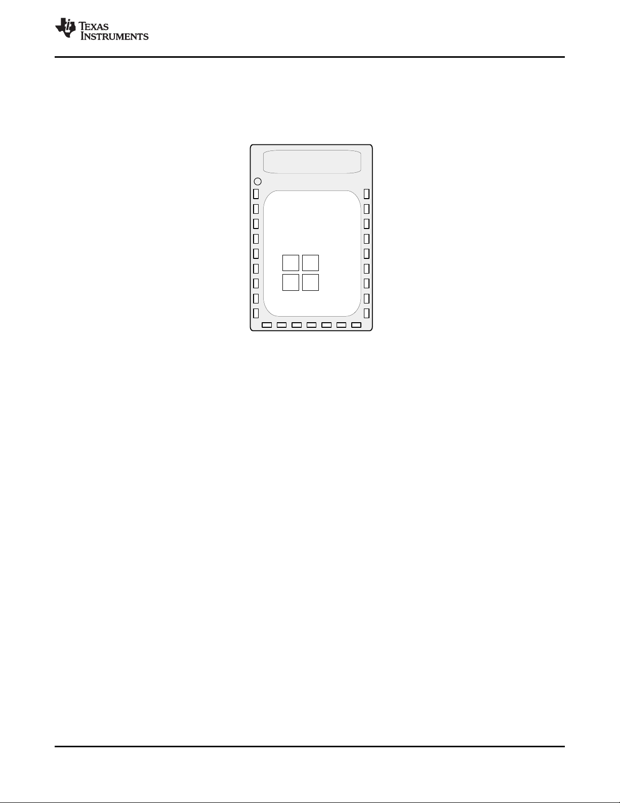
4 Terminal Configuration and Functions
Section 4.1 shows pin assignments for the CC2650MODA device.
4.1 Module Pin Diagram
CC2650MODA
SWRS187D –AUGUST 2016–REVISED JULY 2019
(1) The following I/O pins marked in bold in the pinout have high-drive capabilities:
• DIO 2
• DIO 3
• DIO 4
• JTAG_TMS
• DIO 5/JTAG_TDO
• DIO 6/JTAG_TDI
(2) The following I/O pins marked in italics in the pinout have analog capabilities:
• DIO 7
• DIO 8
• DIO 9
• DIO 10
• DIO 11
• DIO 12
• DIO 13
• DIO 14
Figure 4-1. CC2650MODA MOH Package
(16.9-mm × 11-mm) Module Pinout
Terminal Configuration and FunctionsCopyright © 2016–2019, Texas Instruments Incorporated
7
Submit Documentation Feedback
Product Folder Links: CC2650MODA
Page 8
CC2650MODA
SWRS187D –AUGUST 2016–REVISED JULY 2019
www.ti.com
4.2 Pin Functions
Table 4-1 describes the CC2650MODA pins.
Table 4-1. Signal Descriptions – MOH Package
PIN NAME PIN NO. PIN TYPE DESCRIPTION
DIO_0 4 Digital I/O GPIO, Sensor Controller
DIO_1 5 Digital I/O GPIO, Sensor Controller
DIO_2 6 Digital I/O GPIO, Sensor Controller, high-drive capability
DIO_3 7 Digital I/O GPIO, Sensor Controller, high-drive capability
DIO_4 8 Digital I/O GPIO, Sensor Controller, high-drive capability
DIO_5/JTAG_TDO 11 Digital I/O GPIO, high-drive capability, JTAG_TDO
DIO_6/JTAG_TDI 12 Digital I/O GPIO, high-drive capability, JTAG_TDI
DIO_7 14 Digital I/O, Analog I/O GPIO, Sensor Controller, analog
DIO_8 15 Digital I/O, Analog I/O GPIO, Sensor Controller, analog
DIO_9 16 Digital I/O, Analog I/O GPIO, Sensor Controller, analog
DIO_10 17 Digital I/O, Analog I/O GPIO, Sensor Controller, analog
DIO_11 18 Digital I/O, Analog I/O GPIO, Sensor Controller, analog
DIO_12 19 Digital I/O, Analog I/O GPIO, Sensor Controller, analog
DIO_13 20 Digital I/O, Analog I/O GPIO, Sensor Controller, analog
DIO_14 21 Digital I/O, Analog I/O GPIO, Sensor Controller, analog
EGP G1, G2, G3, G4 Power Ground – Exposed ground pad
GND 1, 3, 25 — Ground
JTAG_TCK 10 Digital I/O JTAG TCKC
JTAG_TMS 9 Digital I/O JTAG TMSC, high-drive capability
NC 2, 24 NC Not Connected—TI recommends leaving these pins floating
nRESET 13 Digital input Reset, active low. No internal pullup
VDD 22, 23 Power 1.8-V to 3.8-V main chip supply
8
Terminal Configuration and Functions Copyright © 2016–2019, Texas Instruments Incorporated
Submit Documentation Feedback
Product Folder Links: CC2650MODA
Page 9
CC2650MODA
www.ti.com
SWRS187D –AUGUST 2016–REVISED JULY 2019
5 Specifications
5.1 Absolute Maximum Ratings
over operating free-air temperature range (unless otherwise noted)
VDD Supply voltage –0.3 4.1 V
Voltage on any digital pin
V
T
(1) Stresses beyond those listed under Absolute Maximum Ratings may cause permanent damage to the device. These are stress ratings
(2) All voltage values are with respect to ground, unless otherwise noted.
(3) Including analog capable DIO.
Voltage on ADC input
in
Input RF level 5 dBm
Storage temperature –40 85 °C
stg
only, and functional operation of the device at these or any other conditions beyond those indicated under Recommended Operating
Conditions is not implied. Exposure to absolute-maximum-rated conditions for extended periods may affect device reliability.
(3)
Voltage scaling enabled –0.3 VDD
Voltage scaling disabled, VDD as reference –0.3 VDD / 2.9
5.2 ESD Ratings
Human body model (HBM), per ANSI/ESDA/JEDEC
(1)
V
ESD
(1) JEDEC document JEP155 states that 500-V HBM allows safe manufacturing with a standard ESD control process.
(2) JEDEC document JEP157 states that 250-V CDM allows safe manufacturing with a standard ESD control process.
Electrostatic discharge
JS001
Charged device model (CDM), per JESD22-C101
(1)(2)
MIN MAX UNIT
–0.3 VDD + 0.3, max 4.1 V
VALUE UNIT
All pins ±1000
(2)
RF pins ±500
Non-RF pins ±500
V
VVoltage scaling disabled, internal reference –0.3 1.49
5.3 Recommended Operating Conditions
MIN MAX UNIT
Ambient temperature –40 85 °C
Operating supply voltage (VDD)
For operation in battery-powered and 3.3-V systems
(internal DC-DC can be used to minimize power
consumption)
1.8 3.8 V
Submit Documentation Feedback
Product Folder Links: CC2650MODA
SpecificationsCopyright © 2016–2019, Texas Instruments Incorporated
9
Page 10
CC2650MODA
SWRS187D –AUGUST 2016–REVISED JULY 2019
5.4 Power Consumption Summary
Tc= 25°C, VDD= 3.0 V with internal DC-DC converter, unless otherwise noted
PARAMETER TEST CONDITIONS MIN TYP MAX UNIT
Reset. RESET_N pin asserted or VDD below Power-onReset threshold
Shutdown. No clocks running, no retention 150
Standby. With RTC, CPU, RAM and (partial) register
retention. RCOSC_LF
Standby. With RTC, CPU, RAM and (partial) register
retention. XOSC_LF
I
core
Core current
consumption
Peripheral Current Consumption (Adds to core current I
Peripheral power
domain
Serial power domain Delta current with domain enabled 13
RF core
I
peri
µDMA Delta current with clock enabled, module idle 130
Timers Delta current with clock enabled, module idle 113
I2C Delta current with clock enabled, module idle 12
I2S Delta current with clock enabled, module idle 36
SSI Delta current with clock enabled, module idle 93
UART Delta current with clock enabled, module idle 164
(1) I
is not supported in Standby or Shutdown.
peri
Standby. With Cache, RTC, CPU, RAM and (partial)
register retention. RCOSC_LF
Standby. With Cache, RTC, CPU, RAM and (partial)
register retention. XOSC_LF
Idle. Supply systems and RAM powered. 550
Active. Core running CoreMark
Radio RX 6.2
Radio TX, 5-dBm output power 9.4
for each peripheral unit activated)
core
Delta current with domain enabled 20
Delta current with power domain enabled, clock
enabled, RF Core Idle
www.ti.com
100
nA
1
1.2
2.5
µA
2.7
1.45 mA +
31 µA/MHz
mARadio TX, 0-dBm output power 6.8
(1)
237
µA
5.5 General Characteristics
Tc= 25°C, VDD= 3.0 V, unless otherwise noted
PARAMETER TEST CONDITIONS MIN TYP MAX UNIT
FLASH MEMORY
Supported flash erase cycles before
failure
Flash page/sector erase current Average delta current 12.6 mA
Flash page/sector erase time
(1)
Flash page/sector size 4 KB
Flash write current Average delta current, 4 bytes at a time 8.15 mA
Flash write time
(1)
4 bytes at a time 8 µs
(1) This number is dependent on flash aging and will increase over time and erase cycles.
10
Specifications Copyright © 2016–2019, Texas Instruments Incorporated
Submit Documentation Feedback
Product Folder Links: CC2650MODA
100 k Cycles
8 ms
Page 11
CC2650MODA
www.ti.com
SWRS187D –AUGUST 2016–REVISED JULY 2019
5.6 Antenna
Tc= 25°C, VDD= 3.0 V, unless otherwise noted.
PARAMETER TEST CONDITIONS MIN TYP MAX UNIT
Polarization Linear
Peak Gain 2450 MHz 1.26 dBi
Efficiency 2450 MHz 57%
5.7 1-Mbps GFSK (Bluetooth low energy) – RX
RF performance is specified in a single ended 50-Ω reference plane at the antenna feeding point with Tc= 25°C,
VDD= 3.0 V, fRF= 2440 MHz, unless otherwise noted.
PARAMETER TEST CONDITIONS MIN TYP MAX UNIT
Receiver sensitivity BER = 10
Receiver saturation BER = 10
Frequency error tolerance
Difference between center frequency of the received RF signal
and local oscillator frequency.
Data rate error tolerance –750 750 ppm
Co-channel rejection
Selectivity, ±1 MHz
Selectivity, ±2 MHz
Selectivity, ±3 MHz
Selectivity, ±4 MHz
(1)
(1)
(1)
(1)
(1)
Selectivity, ±5 MHz or more
Selectivity, Image frequency
Selectivity,
Image frequency ±1 MHz
Out-of-band blocking
(3)
Wanted signal at –67 dBm, modulated interferer in channel,
BER = 10
Wanted signal at –67 dBm, modulated interferer at ±1 MHz,
BER = 10
Wanted signal at –67 dBm, modulated interferer at ±2 MHz,
BER = 10
Wanted signal at –67 dBm, modulated interferer at ±3 MHz,
BER = 10
Wanted signal at –67 dBm, modulated interferer at ±4 MHz,
BER = 10
Wanted signal at –67 dBm, modulated interferer at ≥ ±5 MHz,
(1)
BER = 10
Wanted signal at –67 dBm, modulated interferer at image
(1)
frequency, BER = 10
Wanted signal at –67 dBm, modulated interferer at ±1 MHz from
(1)
image frequency, BER = 10
30 MHz to 2000 MHz –20 dBm
Out-of-band blocking 2003 MHz to 2399 MHz –5 dBm
Out-of-band blocking 2484 MHz to 2997 MHz –8 dBm
Out-of-band blocking 3000 MHz to 12.75 GHz –8 dBm
Intermodulation
Spurious emissions,
30 MHz to 1000 MHz
Spurious emissions,
1 GHz to 12.75 GHz
Wanted signal at 2402 MHz, –64 dBm. Two interferers at 2405
and 2408 MHz respectively, at the given power level
Conducted measurement in a 50-Ω single-ended load. Suitable
for systems targeting compliance with EN 300 328, EN 300 440
class 2, FCC CFR47, Part 15 and ARIB STD-T-66
Conducted measurement in a 50-Ω single-ended load. Suitable
for systems targeting compliance with EN 300 328, EN 300 440
class 2, FCC CFR47, Part 15 and ARIB STD-T-66
RSSI dynamic range 70 dB
RSSI accuracy ±4 dB
(1) Numbers given as I/C dB
(2) X / Y, where X is +N MHz and Y is –N MHz
(3) Excluding one exception at F
wanted
–3
–3
–3
–3
–3
–3
–3
–3
–3
–3
/ 2, per Bluetooth Specification
–97 dBm
4 dBm
–350 350 kHz
–6 dB
(2)
7 / 3
(2)
29 / 23
(2)
38 / 26
(2)
42 / 29
32 dB
23 dB
(2)
3 / 26
–34 dBm
–71 dBm
–62 dBm
dB
dB
dB
dB
dB
Submit Documentation Feedback
Product Folder Links: CC2650MODA
SpecificationsCopyright © 2016–2019, Texas Instruments Incorporated
11
Page 12
CC2650MODA
SWRS187D –AUGUST 2016–REVISED JULY 2019
www.ti.com
5.8 1-Mbps GFSK (Bluetooth low energy) – TX
RF performance is specified in a single ended 50-Ω reference plane at the antenna feeding point with Tc= 25°C,
VDD= 3.0 V, fRF= 2440 MHz, unless otherwise noted.
PARAMETER TEST CONDITIONS MIN TYP MAX UNIT
Output power, highest setting 5 dBm
Output power, lowest setting –21 dBm
f < 1 GHz, outside restricted bands –43
Spurious emission conducted
measurement
(1) Suitable for systems targeting compliance with worldwide radio-frequency regulations ETSI EN 300 328 and EN 300 440 Class 2
(Europe), FCC CFR47 Part 15 (US), and ARIB STD-T66 (Japan)
(1)
f < 1 GHz, restricted bands ETSI –58
f < 1 GHz, restricted bands FCC –57
f > 1 GHz, including harmonics –45
dBm
5.9 IEEE 802.15.4 (Offset Q-PSK DSSS, 250 kbps) – RX
RF performance is specified in a single ended 50-Ω reference plane at the antenna feeding point with Tc= 25°C,
VDD= 3.0 V, unless otherwise noted.
PARAMETER TEST CONDITIONS MIN TYP MAX UNIT
Receiver sensitivity PER = 1% –100 dBm
Receiver saturation PER = 1% –7 dBm
Adjacent channel rejection
Alternate channel rejection
Channel rejection, ±15 MHz or
more
Blocking and desensitization,
5 MHz from upper band edge
Blocking and desensitization,
10 MHz from upper band edge
Blocking and desensitization,
20 MHz from upper band edge
Blocking and desensitization,
50 MHz from upper band edge
Blocking and desensitization,
–5 MHz from lower band edge
Blocking and desensitization,
–10 MHz from lower band edge
Blocking and desensitization,
–20 MHz from lower band edge
Blocking and desensitization,
–50 MHz from lower band edge
Spurious emissions,
30 MHz to 1000 MHz
Spurious emissions,
1 GHz to 12.75 GHz
Frequency error tolerance
RSSI dynamic range 100 dB
RSSI accuracy ±4 dB
Wanted signal at –82 dBm, modulated interferer at ±5 MHz,
PER = 1%
Wanted signal at –82 dBm, modulated interferer at ±10 MHz,
PER = 1%
Wanted signal at –82 dBm, undesired signal is IEEE 802.15.4
modulated channel, stepped through all channels 2405 to
2480 MHz, PER = 1%
Wanted signal at –97 dBm (3 dB above the sensitivity level),
CW jammer, PER = 1%
Wanted signal at –97 dBm (3 dB above the sensitivity level),
CW jammer, PER = 1%
Wanted signal at –97 dBm (3 dB above the sensitivity level),
CW jammer, PER = 1%
Wanted signal at –97 dBm (3 dB above the sensitivity level),
CW jammer, PER = 1%
Wanted signal at –97 dBm (3 dB above the sensitivity level),
CW jammer, PER = 1%
Wanted signal at –97 dBm (3 dB above the sensitivity level),
CW jammer, PER = 1%
Wanted signal at –97 dBm (3 dB above the sensitivity level),
CW jammer, PER = 1%
Wanted signal at –97 dBm (3 dB above the sensitivity level),
CW jammer, PER = 1%
Conducted measurement in a 50-Ω single-ended load.
Suitable for systems targeting compliance with EN 300 328,
EN 300 440 class 2, FCC CFR47, Part 15 and ARIB STD-T66
Conducted measurement in a 50-Ω single-ended load.
Suitable for systems targeting compliance with EN 300 328,
EN 300 440 class 2, FCC CFR47, Part 15 and ARIB STD-T66
Difference between center frequency of the received RF
signal and local oscillator frequency
35 dB
52 dB
57 dB
64 dB
64 dB
65 dB
68 dB
63 dB
63 dB
65 dB
67 dB
–71 dBm
–62 dBm
>200 ppm
12
Specifications Copyright © 2016–2019, Texas Instruments Incorporated
Submit Documentation Feedback
Product Folder Links: CC2650MODA
Page 13
CC2650MODA
www.ti.com
SWRS187D –AUGUST 2016–REVISED JULY 2019
5.10 IEEE 802.15.4 (Offset Q-PSK DSSS, 250 kbps) – TX
RF performance is specified in a single ended 50-Ω reference plane at the antenna feeding point with Tc= 25°C,
VDD= 3.0 V, unless otherwise noted.
PARAMETER TEST CONDITIONS MIN TYP MAX UNIT
Output power, highest setting 5 dBm
Output power, lowest setting –21 dBm
Error vector magnitude At maximum output power 2%
f < 1 GHz, outside restricted bands –43
Spurious emission conducted
measurement
(1) Suitable for systems targeting compliance with worldwide radio-frequency regulations ETSI EN 300 328 and EN 300 440 Class 2
(Europe), FCC CFR47 Part 15 (US), and ARIB STD-T66 (Japan)
(1)
f < 1 GHz, restricted bands ETSI –58
f < 1 GHz, restricted bands FCC –57
f > 1 GHz, including harmonics –45
dBm
5.11 24-MHz Crystal Oscillator (XOSC_HF)
(1)
over operating free-air temperature range (unless otherwise noted)
PARAMETER TEST CONDITIONS MIN TYP MAX UNIT
Crystal frequency 24 MHz
Crystal frequency tolerance
Start-up time
(1) Probing or otherwise stopping the XTAL while the DC-DC converter is enabled may cause permanent damage to the device.
(2) Includes initial tolerance of the crystal, drift over temperature, aging and frequency pulling due to incorrect load capacitance. As per
Bluetooth and IEEE 802.15.4 specification
(3) Kick-started based on a temperature and aging compensated RCOSC_HF using precharge injection
(3)
(2)
–40 40 ppm
150 µs
5.12 32.768-kHz Crystal Oscillator (XOSC_LF)
over operating free-air temperature range (unless otherwise noted)
PARAMETER TEST CONDITIONS MIN TYP MAX UNIT
Crystal frequency 32.768 kHz
Initial crystal frequency tolerance, Bluetooth
low energy applications
Crystal aging -3 3 ppm/year
Tc= 25°C
–20 20 ppm
5.13 48-MHz RC Oscillator (RCOSC_HF)
Tc= 25°C, VDD= 3.0 V, unless otherwise noted
PARAMETER TEST CONDITIONS MIN TYP MAX UNIT
Frequency 48 MHz
Uncalibrated frequency accuracy ±1%
Calibrated frequency accuracy
Start-up time 5 µs
(1) Accuracy relatively to the calibration source (XOSC_HF).
(1)
±0.25%
5.14 32-kHz RC Oscillator (RCOSC_LF)
Tc= 25°C, VDD= 3.0 V, unless otherwise noted
PARAMETER TEST CONDITIONS MIN TYP MAX UNIT
Calibrated frequency 32.8 kHz
Temperature coefficient 50 ppm/°C
SpecificationsCopyright © 2016–2019, Texas Instruments Incorporated
Submit Documentation Feedback
Product Folder Links: CC2650MODA
13
Page 14
CC2650MODA
SWRS187D –AUGUST 2016–REVISED JULY 2019
5.15 ADC Characteristics
Tc= 25°C, VDD= 3.0 V and voltage scaling enabled, unless otherwise noted
PARAMETER TEST CONDITIONS MIN TYP MAX UNIT
Input voltage range 0 V
Resolution 12 Bits
Sample rate 200 ksps
Offset Internal 4.3-V equivalent reference
Gain error Internal 4.3-V equivalent reference
(3)
DNL
INL
(4)
Differential nonlinearity >–1 LSB
Integral nonlinearity ±3 LSB
Internal 4.3-V equivalent reference
9.6-kHz input tone
ENOB Effective number of bits
Internal 1.44-V reference, voltage scaling disabled,
32 samples average, 200 ksps, 300-Hz input tone
Internal 4.3-V equivalent reference
9.6-kHz input tone
THD
Total harmonic
distortion
Internal 1.44-V reference, voltage scaling disabled,
32 samples average, 200 ksps, 300-Hz input tone
Internal 4.3-V equivalent reference
9.6-kHz input tone
SINAD
and SNDR
Signal-to-noise and
distortion ratio
Internal 1.44-V reference, voltage scaling disabled,
32 samples average, 200 ksps, 300-Hz input tone
Internal 4.3-V equivalent reference
9.6-kHz input tone
SFDR
Spurious-free dynamic
range
Internal 1.44-V reference, voltage scaling disabled, 32
samples average, 200 ksps, 300-Hz input tone
Conversion time Serial conversion, time-to-output, 24-MHz clock 50
Current consumption Internal 4.3-V equivalent reference
Current consumption VDD as reference 0.75 mA
Equivalent fixed internal reference (input voltage
scaling enabled). For best accuracy, the ADC
Reference voltage
conversion should be initiated through the TI-RTOS™
API to include the gain or offset compensation factors
stored in FCFG1.
Fixed internal reference (input voltage scaling
disabled). For best accuracy, the ADC conversion
Reference voltage
should be initiated through the TI-RTOS API to include
the gain or offset compensation factors stored in
FCFG1. This value is derived from the scaled value
Reference voltage
Reference voltage
(4.3 V) as follows: V
VDD as reference (Also known as RELATIVE) (input
voltage scaling enabled)
VDD as reference (Also known as RELATIVE) (input
voltage scaling disabled)
= 4.3 V × 1408 / 4095
ref
200 ksps, voltage scaling enabled. Capacitive input,
Input Impedance
input impedance depends on sampling frequency and
sampling time
(1) Using IEEE Std 1241™-2010 for terminology and test methods.
(2) Input signal scaled down internally before conversion, as if voltage range was 0 to 4.3 V.
(3) No missing codes. Positive DNL typically varies from +0.3 to +3.5 depending on device, see Figure 5-24.
(4) For a typical example, see Figure 5-25.
(5) Applied voltage must be within absolute maximum ratings (see Section 5.1) at all times.
(2)
(2)
(2)
, 200 ksps,
(2)
, 200 ksps,
(2)
, 200 ksps,
(2)
, 200 ksps,
(2)
(1)
4.3
VDD V
VDD / 2.82
www.ti.com
V
DD
2 LSB
2.4 LSB
9.8
BitsVDD as reference, 200 ksps, 9.6-kHz input tone 10
11.1
–65
dBVDD as reference, 200 ksps, 9.6-kHz input tone –69
–71
60
dBVDD as reference, 200 ksps, 9.6-kHz input tone 63
69
67
dBVDD as reference, 200 ksps, 9.6-kHz input tone 72
73
clockcycles
0.66 mA
(2)(5)
V
1.48 V
(5)
V
>1 MΩ
14
Specifications Copyright © 2016–2019, Texas Instruments Incorporated
Submit Documentation Feedback
Product Folder Links: CC2650MODA
Page 15
CC2650MODA
www.ti.com
SWRS187D –AUGUST 2016–REVISED JULY 2019
5.16 Temperature Sensor
Tc= 25°C, VDD= 3.0 V, unless otherwise noted
PARAMETER TEST CONDITIONS MIN TYP MAX UNIT
Resolution 4 °C
Range –40 85 °C
Accuracy ±5 °C
Supply voltage coefficient
(1) Automatically compensated when using supplied driver libraries.
(1)
3.2 °C/V
5.17 Battery Monitor
Tc= 25°C, VDD= 3.0 V, unless otherwise noted
PARAMETER TEST CONDITIONS MIN TYP MAX UNIT
Resolution 50 mV
Range 1.8 3.8 V
Accuracy 13 mV
5.18 Continuous Time Comparator
Tc= 25°C, VDD= 3.0 V, unless otherwise noted
PARAMETER TEST CONDITIONS MIN TYP MAX UNIT
Input voltage range 0 V
External reference voltage 0 V
Internal reference voltage DCOUPL as reference 1.27 V
Offset 3 mV
Hysteresis <2 mV
Decision time Step from –10 mV to +10 mV 0.72 µs
Current consumption when enabled
(1) Additionally, the bias module must be enabled when running in standby mode.
(1)
8.6 µA
DD
DD
V
V
5.19 Low-Power Clocked Comparator
Tc= 25°C, VDD= 3.0 V, unless otherwise noted
PARAMETER TEST CONDITIONS MIN TYP MAX UNIT
Input voltage range 0 VDD V
Clock frequency 32 kHz
Internal reference voltage, VDD / 2 1.49–1.51 V
Internal reference voltage, VDD / 3 1.01–1.03 V
Internal reference voltage, VDD / 4 0.78–0.79 V
Internal reference voltage, DCOUPL / 1 1.25–1.28 V
Internal reference voltage, DCOUPL / 2 0.63–0.65 V
Internal reference voltage, DCOUPL / 3 0.42–0.44 V
Internal reference voltage, DCOUPL / 4 0.33–0.34 V
Offset <2 mV
Hysteresis <5 mV
Decision time Step from –50 mV to +50 mV <1 clock-cycle
Current consumption when enabled 362 nA
Submit Documentation Feedback
Product Folder Links: CC2650MODA
SpecificationsCopyright © 2016–2019, Texas Instruments Incorporated
15
Page 16
CC2650MODA
SWRS187D –AUGUST 2016–REVISED JULY 2019
www.ti.com
5.20 Programmable Current Source
Tc= 25°C, VDD= 3.0 V, unless otherwise noted.
PARAMETER TEST CONDITIONS MIN TYP MAX UNIT
Current source programmable output range 0.25–20 µA
Resolution 0.25 µA
Current consumption
(1) Additionally, the bias module must be enabled when running in standby mode.
(1)
Including current source at maximum
programmable output
23 µA
5.21 DC Characteristics
PARAMETER TEST CONDITIONS MIN TYP MAX UNIT
TA= 25°C, VDD= 1.8 V
GPIO VOH at 8-mA load IOCURR = 2, high-drive GPIOs only 1.32 1.54 V
GPIO VOL at 8-mA load IOCURR = 2, high-drive GPIOs only 0.26 0.32 V
GPIO VOH at 4-mA load IOCURR = 1 1.32 1.58 V
GPIO VOL at 4-mA load IOCURR = 1 0.21 0.32 V
GPIO pullup current Input mode, pullup enabled, Vpad = 0 V 71.7 µA
GPIO pulldown current Input mode, pulldown enabled, Vpad = VDD 21.1 µA
GPIO high/low input transition,
no hysteresis
GPIO low-to-high input transition,
with hysteresis
GPIO high-to-low input transition,
with hysteresis
GPIO input hysteresis IH = 1, difference between 0 → 1 and 1 → 0 points 0.33 V
TA= 25°C, VDD= 3.0 V
GPIO VOH at 8-mA load IOCURR = 2, high-drive GPIOs only 2.68 V
GPIO VOL at 8-mA load IOCURR = 2, high-drive GPIOs only 0.33 V
GPIO VOH at 4-mA load IOCURR = 1 2.72 V
GPIO VOL at 4-mA load IOCURR = 1 0.28 V
TA= 25°C, VDD= 3.8 V
GPIO pullup current Input mode, pullup enabled, Vpad = 0 V 277 µA
GPIO pulldown current Input mode, pulldown enabled, Vpad = VDD 113 µA
GPIO high/low input transition,
no hysteresis
GPIO low-to-high input transition,
with hysteresis
GPIO high-to-low input transition,
with hysteresis
GPIO input hysteresis IH = 1, difference between 0 → 1 and 1 → 0 points 0.4 V
TA= 25°C
VIH
VIL
IH = 0, transition between reading 0 and reading 1 0.88 V
IH = 1, transition voltage for input read as 0 → 1 1.07 V
IH = 1, transition voltage for input read as 1 → 0 0.74 V
IH = 0, transition between reading 0 and reading 1 1.67 V
IH = 1, transition voltage for input read as 0 → 1 1.94 V
IH = 1, transition voltage for input read as 1 → 0 1.54 V
Lowest GPIO input voltage reliably interpreted as a
«High»
Highest GPIO input voltage reliably interpreted as a
«Low»
0.2 VDD
0.8 VDD
16
Specifications Copyright © 2016–2019, Texas Instruments Incorporated
Submit Documentation Feedback
Product Folder Links: CC2650MODA
Page 17

CC2650MODA
www.ti.com
SWRS187D –AUGUST 2016–REVISED JULY 2019
5.22 Thermal Resistance Characteristics for MOH Package
NAME DESCRIPTION °C/W
RΘ
RΘ
RΘ
RΘ
Psi
Psi
JC
JB
JA
JMA
JT
JB
Junction-to-case 20.0
Junction-to-board 15.3
Junction-to-free air 29.6 0
Junction-to-moving air 25.0 1
Junction-to-package top 8.8 0
Junction-to-board 14.8 0
(1) °C/W = degrees Celsius per watt.
(2) These values are based on a JEDEC-defined 2S2P system (with the exception of the Theta JC [RΘJC] value, which is based on a
JEDEC-defined 1S0P system) and will change based on environment as well as application. For more information, see these
EIA/JEDEC standards:
• JESD51-2, Integrated Circuits Thermal Test Method Environmental Conditions - Natural Convection (Still Air)
• JESD51-3, Low Effective Thermal Conductivity Test Board for Leaded Surface Mount Packages
• JESD51-7, High Effective Thermal Conductivity Test Board for Leaded Surface Mount Packages
• JESD51-9, Test Boards for Area Array Surface Mount Package Thermal Measurements
Power dissipation of 2 W and an ambient temperature of 70ºC is assumed.
(3) m/s = meters per second.
(1) (2)
AIR FLOW (m/s)
5.23 Timing Requirements
MIN NOM MAX UNIT
Rising supply-voltage slew rate 0 100 mV/µs
Falling supply-voltage slew rate 0 20 mV/µs
Falling supply-voltage slew rate, with low-power flash settings
Positive temperature gradient in standby
CONTROL INPUT AC CHARACTERISTICS
(2)
(3)
RESET_N low duration 1 µs
SYNCHRONOUS SERIAL INTERFACE (SSI)
S1 (SLAVE)
(5)
S2
(5)
S3
(5)
t
clk_per
t
clk_high
t
clk_low
(4)
(1) For smaller coin cell batteries, with high worst-case end-of-life equivalent source resistance, a 22-µF VDD input capacitor (see
Section 7.1.1) must be used to ensure compliance with this slew rate.
(2) Applications using RCOSC_LF as sleep timer must also consider the drift in frequency caused by a change in temperature (see
Section 5.14).
(3) TA= –40°C to +85°C, VDD= 1.7 V to 3.8 V, unless otherwise noted.
(4) Tc= 25°C, VDD= 3.0 V, unless otherwise noted. Device operating as slave. For SSI master operation, see Section 5.24.
(5) Refer to the SSI timing diagrams Figure 5-1, Figure 5-2, and Figure 5-3.
(1)
No limitation for negative
temperature gradient, or
outside standby mode
SSIClk period 12 65024
SSIClk high time 0.5 t
SSIClk low time 0.5 t
3 mV/µs
5 °C/s
System
clocks
clk_per
clk_per
(3)
5.24 Switching Characteristics
Measured on the TI CC2650EM-5XD reference design with Tc= 25°C, VDD= 3.0 V, unless otherwise noted.
PARAMETER TEST CONDITIONS MIN TYP MAX UNIT
WAKEUP AND TIMING
Idle → Active 14 µs
Standby → Active 151 µs
Shutdown → Active 1015 µs
SpecificationsCopyright © 2016–2019, Texas Instruments Incorporated
Submit Documentation Feedback
Product Folder Links: CC2650MODA
17
Page 18

0
SSIClk
SSIFss
SSITx
SSIRx
MSB LSB
MSB LSB
S2
S3
S1
8-bit control
4 to 16 bits output data
SSIClk
SSIFss
SSITx
SSIRx
MSB LSB
S2
S3
S1
4 to 16 bits
CC2650MODA
SWRS187D –AUGUST 2016–REVISED JULY 2019
Switching Characteristics (continued)
Measured on the TI CC2650EM-5XD reference design with Tc= 25°C, VDD= 3.0 V, unless otherwise noted.
PARAMETER TEST CONDITIONS MIN TYP MAX UNIT
SYNCHRONOUS SERIAL INTERFACE (SSI)
S1 (TX only)
S1 (TX and RX)
(2)
S2
(2)
S3
(1) Device operating as master. For SSI slave operation, see Section 5.23.
(2) Refer to SSI timing diagrams Figure 5-1, Figure 5-2, and Figure 5-3.
(2)
t
(SSIClk period) One-way communication to SLAVE 4 65024
clk_per
(2)
t
(SSIClk period) Normal duplex operation 8 65024
clk_per
t
(SSIClk high time) 0.5 t
clk_high
t
(SSIClk low time) 0.5 t
clk_low
(1)
www.ti.com
System
clocks
System
clocks
clk_per
clk_per
Figure 5-1. SSI Timing for TI Frame Format (FRF = 01), Single Transfer Timing Measurement
Figure 5-2. SSI Timing for MICROWIRE Frame Format (FRF = 10), Single Transfer
18
Specifications Copyright © 2016–2019, Texas Instruments Incorporated
Submit Documentation Feedback
Product Folder Links: CC2650MODA
Page 19

SSIClk
(SPO = 1)
SSITx
(Master)
SSIRx
(Slave)
LSB
SSIClk
(SPO = 0)
S2
S1
SSIFss
LSB
S3
MSB
MSB
www.ti.com
CC2650MODA
SWRS187D –AUGUST 2016–REVISED JULY 2019
Figure 5-3. SSI Timing for SPI Frame Format (FRF = 00), With SPH = 1
Submit Documentation Feedback
Product Folder Links: CC2650MODA
SpecificationsCopyright © 2016–2019, Texas Instruments Incorporated
19
Page 20

Frequency (MHz)
Sensitivity Level (dBm)
2400 2410 2420 2430 2440 2450 2460 2470 2480
-101
-100
-99
-98
-97
-96
-95
D008
Sensitivity
Frequency (MHz)
Sensitivity Level (dBm)
2400 2410 2420 2430 2440 2450 2460 2470 2480
-99
-98.5
-98
-97.5
-97
-96.5
-96
-95.5
-95
D009
Sensitivity
VDDS (V)
Sensitivity (dBm)
1.8 2.3 2.8 3.3 3.8
-101
-100
-99
-98
-97
-96
-95
D006
BLE Sensitivity
VDDS (V)
Sensitivity (dBm)
1.9 2.4 2.9 3.4 3.8
-101
-100
-99
-98
-97
-96
-95
D007
IEEE 802.15.4 Sensitivity
Temperature (qC)
Sensitivity (dBm)
-40 -30 -20 -10 0 10 20 30 40 50 60 70 80
-99
-98
-97
-96
-95
-94
-93
D004
Sensitivity
Temperature (qC)
Sensitivity (dBm)
-40 -30 -20 -10 0 10 20 30 40 50 60 70 80
-103
-102
-101
-100
-99
-98
-97
-96
-95
D005
Sensitivity
CC2650MODA
SWRS187D –AUGUST 2016–REVISED JULY 2019
www.ti.com
5.25 Typical Characteristics
This section contains typical performance plots measured on the CC2650F128RHB device. They are published in the
CC2650 data sheet, and the plots relevant for the CC2650MODA device are repeated here. RF performance is specified in a
single-ended 50-Ω reference plane at the antenna feeding point with Tc= 25°C and VDD= 3.0 V, unless otherwise noted.
Figure 5-4. Bluetooth low energy Sensitivity vs Temperature
Figure 5-6. Bluetooth low energy Sensitivity
vs Supply Voltage (VDD)
Figure 5-5. IEEE 802.15.4 Sensitivity vs Temperature
Figure 5-7. IEEE 802.15.4 Sensitivity
vs Supply Voltage (VDD)
20
Specifications Copyright © 2016–2019, Texas Instruments Incorporated
Figure 5-8. IEEE 802.15.4 Sensitivity
vs Channel Frequency
Submit Documentation Feedback
Product Folder Links: CC2650MODA
Figure 5-9. Bluetooth low energy Sensitivity
vs Channel Frequency
Page 21

Voltage (V)
Current Consumption (mA)
1.75 2 2.25 2.5 2.75 3 3.25 3.5 3.75 4 4.25 4.5
4.5
5
5.5
6
6.5
7
7.5
8
8.5
9
9.5
10
10.5
D014
Temperature (qC)
RX Current (mA)
-40 -30 -20 -10 0 10 20 30 40 50 60 70 80
5.5
5.6
5.7
5.8
5.9
6
6.1
6.2
6.3
6.4
6.5
6.6
6.7
6.8
6.9
7
D015
RX Current
Frequency (MHz)
Output Power (dBm)
2400 2410 2420 2430 2440 2450 2460 2470 2480
-1
0
1
2
3
4
5
6
7
8
D012
5-dBm setting
VDDS (V)
TX Current (mA)
1.8 2 2.2 2.4 2.6 2.8 3 3.2 3.4 3.6 3.8
4
5
6
7
8
9
10
11
12
13
14
15
16
D013
5-dBm Setting
Temperature (qC)
Output Power (dBm)
-40 -30 -20 -10 0 10 20 30 40 50 60 70 80
0
1
2
3
4
5
6
D010
5-dBm Setting
VDDS (V)
Output power (dBm)
1.8 2.3 2.8 3.3 3.8
0
1
2
3
4
5
6
D011
5-dBm Setting
CC2650MODA
www.ti.com
SWRS187D –AUGUST 2016–REVISED JULY 2019
Typical Characteristics (continued)
This section contains typical performance plots measured on the CC2650F128RHB device. They are published in the
CC2650 data sheet, and the plots relevant for the CC2650MODA device are repeated here. RF performance is specified in a
single-ended 50-Ω reference plane at the antenna feeding point with Tc= 25°C and VDD= 3.0 V, unless otherwise noted.
Figure 5-10. TX Output Power vs Temperature Figure 5-11. TX Output Power vs Supply Voltage (VDD)
Figure 5-12. TX Output Power
vs Channel Frequency
Figure 5-14. RX Mode Current vs Supply Voltage (VDD) Figure 5-15. RX Mode Current Consumption vs Temperature
Submit Documentation Feedback
Product Folder Links: CC2650MODA
Figure 5-13. TX Current Consumption
vs Supply Voltage (VDD)
SpecificationsCopyright © 2016–2019, Texas Instruments Incorporated
21
Page 22

Input Frequency (Hz)
Effective Number of Bits
200300 500 1000 2000 5000 10000 20000 100000
9.4
9.6
9.8
10
10.2
10.4
10.6
10.8
11
11.2
11.4
D009
Fs= 200 kHz, No Averaging
Fs= 200 kHz, 32 samples averaging
VDDS (V)
ADC Code
1.8 2.3 2.8 3.3 3.8
1004.8
1005
1005.2
1005.4
1005.6
1005.8
1006
1006.2
1006.4
D012
VDDS (V)
Current Consumption (mA)
1.8 2.3 2.8 3.3 3.8
2
2.5
3
3.5
4
4.5
5
D007
Active Mode Current
Temperature (qC)
Current (uA)
-20 -10 0 10 20 30 40 50 60 70 80
0
0.5
1
1.5
2
2.5
3
3.5
4
D008
Standby Mode Current
Temperature (qC)
Active Mode Current Consumpstion (mA)
-40 -30 -20 -10 0 10 20 30 40 50 60 70 80
2.85
2.9
2.95
3
3.05
3.1
D006
Active Mode Current
Temperature (qC)
TX Current (mA)
-40 -30 -20 -10 0 10 20 30 40 50 60 70 80
0
2
4
6
8
10
12
D016
5-dBm Setting
CC2650MODA
SWRS187D –AUGUST 2016–REVISED JULY 2019
www.ti.com
Typical Characteristics (continued)
This section contains typical performance plots measured on the CC2650F128RHB device. They are published in the
CC2650 data sheet, and the plots relevant for the CC2650MODA device are repeated here. RF performance is specified in a
single-ended 50-Ω reference plane at the antenna feeding point with Tc= 25°C and VDD= 3.0 V, unless otherwise noted.
Figure 5-16. TX Mode Current Consumption vs Temperature
Figure 5-18. Active Mode (MCU Running, No Peripherals)
Current Consumption vs Supply Voltage (VDD)
Figure 5-17. Active Mode (MCU Running, No Peripherals)
Current Consumption vs Temperature
Figure 5-19. Standby Mode Current Consumption
With RCOSC RTC vs Temperature
22
Figure 5-20. SoC ADC Effective Number of Bits vs Input
Frequency (Internal Reference)
Specifications Copyright © 2016–2019, Texas Instruments Incorporated
Submit Documentation Feedback
Product Folder Links: CC2650MODA
Figure 5-21. SoC ADC Output vs Supply Voltage (Fixed Input,
Internal Reference)
Page 23

ADC Code
INL
0 200 400 600 800 1000 1200 1400 1600 1800 2000 2200 2400 2600 2800 3000 3200 3400 3600 3800 4000 4200
-4
-3
-2
-1
0
1
2
3
D011
ADC Code
DNL
0
200
400
600
800
1000
1200
1400
1600
1800
2000
2200
2400
2600
2800
3000
3200
3400
3600
3800
4000
4200
-1.5
-1
-0.5
0
0.5
1
1.5
2
2.5
3
3.5
D010
Temperature (qC)
ADC Code
-40 -30 -20 -10 0 10 20 30 40 50 60 70 80
1004.5
1005
1005.5
1006
1006.5
1007
1007.5
D013
Sampling Frequency (Hz)
ENOB
9.6
9.7
9.8
9.9
10
10.1
10.2
10.3
10.4
10.5
1k 10k 100k 200k
D009A
ENOB Internal Reference (No Averaging)
ENOB Internal Reference (32 Samples Averaging)
CC2650MODA
www.ti.com
SWRS187D –AUGUST 2016–REVISED JULY 2019
Typical Characteristics (continued)
This section contains typical performance plots measured on the CC2650F128RHB device. They are published in the
CC2650 data sheet, and the plots relevant for the CC2650MODA device are repeated here. RF performance is specified in a
single-ended 50-Ω reference plane at the antenna feeding point with Tc= 25°C and VDD= 3.0 V, unless otherwise noted.
Figure 5-22. SoC ADC Output vs Temperature (Fixed Input,
Internal Reference)
Figure 5-24. SoC ADC DNL vs ADC Code (Internal Reference)
Figure 5-23. SoC ADC ENOB vs Sampling Frequency
(Input Frequency = FS / 10)
Figure 5-25. SoC ADC INL vs ADC Code (Internal Reference)
Submit Documentation Feedback
Product Folder Links: CC2650MODA
SpecificationsCopyright © 2016–2019, Texas Instruments Incorporated
23
Page 24

Main CPU
128-KB
Flash
Sensor Controller
cJTAG
20-KB
SRAM
ROM
ARM
Cortex-M3
DC-DC Converter
RF core
ARM
Cortex-M0
DSP Modem
4-KB
SRAM
ROM
Sensor Controller Engine
2× Analog Comparators
12-bit ADC, 200 ks/s
Constant Current Source
SPI / I2C Digital Sensor IF
2-KB SRAM
Time-to-Digital Converter
General Peripherals / Modules
4× 32-bit Timers
2× SSI (SPI, µWire, TI)
Watchdog Timer
Temp. / Batt. Monitor
RTC
I2C
UART
I2S
15 GPIOs
AES
32 ch. µDMA
ADC
ADC
Digital PLL
SimpleLink CC2650MODA Wireless MCU Module
TRNG
8-KB
Cache
24-MHz Crystal
Oscillator
32.768-kHz
Crystal
Oscillator
RF Balun
Copyright © 2017, Texas Instruments Incorporated
CC2650MODA
SWRS187D –AUGUST 2016–REVISED JULY 2019
6 Detailed Description
6.1 Overview
Figure 6-1 shows the core modules of the CC2650MODA device.
6.2 Functional Block Diagram
www.ti.com
24
Detailed Description Copyright © 2016–2019, Texas Instruments Incorporated
Figure 6-1. CC2650MODA Functional Block Diagram
Submit Documentation Feedback
Product Folder Links: CC2650MODA
Page 25

www.ti.com
6.3 Main CPU
The SimpleLink CC2650MODA wireless MCU contains an ARM Cortex-M3 32-bit CPU, which runs the
application and the higher layers of the protocol stack.
The Cortex-M3 processor provides a high-performance, low-cost platform that meets the system
requirements of minimal memory implementation, and low-power consumption, while delivering
outstanding computational performance and exceptional system response to interrupts.
Cortex-M3 features include:
• 32-bit ARM Cortex-M3 architecture optimized for small-footprint embedded applications
• Outstanding processing performance combined with fast interrupt handling
• ARM Thumb®-2 mixed 16- and 32-bit instruction set delivers the high performance expected of a 32-bit
ARM core in a compact memory size usually associated with 8- and 16-bit devices, typically in the
range of a few kilobytes of memory for microcontroller-class applications:
– Single-cycle multiply instruction and hardware divide
– Atomic bit manipulation (bit-banding), delivering maximum memory use and streamlined peripheral
control
– Unaligned data access, enabling data to be efficiently packed into memory
• Fast code execution permits slower processor clock or increases sleep mode time
• Harvard architecture characterized by separate buses for instruction and data
• Efficient processor core, system, and memories
• Hardware division and fast digital-signal-processing oriented multiply accumulate
• Saturating arithmetic for signal processing
• Deterministic, high-performance interrupt handling for time-critical applications
• Enhanced system debug with extensive breakpoint and trace capabilities
• Serial wire trace reduces the number of pins required for debugging and tracing
• Migration from the ARM7™ processor family for better performance and power efficiency
• Optimized for single-cycle flash memory use
• Ultra-low-power consumption with integrated sleep modes
• 1.25 DMIPS per MHz
CC2650MODA
SWRS187D –AUGUST 2016–REVISED JULY 2019
6.4 RF Core
The RF core contains an ARM Cortex-M0 processor that interfaces the analog RF and base-band
circuitries, handles data to and from the system side, and assembles the information bits in a given packet
structure. The RF core offers a high-level, command-based API to the main CPU.
The RF core can autonomously handle the time-critical aspects of the radio protocols (802.15.4 RF4CE
and ZigBee, Bluetooth low energy) thus offloading the main CPU and leaving more resources for the user
application.
The RF core has a dedicated 4-KB SRAM block and runs initially from separate ROM memory. The ARM
Cortex-M0 processor is not programmable by customers.
Submit Documentation Feedback
Product Folder Links: CC2650MODA
Detailed DescriptionCopyright © 2016–2019, Texas Instruments Incorporated
25
Page 26

CC2650MODA
SWRS187D –AUGUST 2016–REVISED JULY 2019
6.5 Sensor Controller
The Sensor Controller contains circuitry that can be selectively enabled in standby mode. The peripherals
in this domain may be controlled by the Sensor Controller Engine, which is a proprietary power-optimized
CPU. This CPU can read and monitor sensors or perform other tasks autonomously, thereby significantly
reducing power consumption and offloading the main Cortex-M3 CPU.
The Sensor Controller is set up using a PC-based configuration tool, called Sensor Controller Studio, and
typical use cases may be (but are not limited to):
• Analog sensors using integrated ADC
• Digital sensors using GPIOs and bit-banged I2C or SPI
• UART communication for sensor reading or debugging
• Capacitive sensing
• Waveform generation
• Pulse counting
• Keyboard scan
• Quadrature decoder for polling rotation sensors
• Oscillator calibration
The peripherals in the Sensor Controller include the following:
• The low-power clocked comparator can be used to wake the device from any state in which the
comparator is active. A configurable internal reference can be used with the comparator. The output of
the comparator can also be used to trigger an interrupt or the ADC.
• Capacitive sensing functionality is implemented through the use of a constant current source, a timeto-digital converter, and a comparator. The continuous time comparator in this block can also be used
as a higher-accuracy alternative to the low-power clocked comparator. The Sensor Controller will take
care of baseline tracking, hysteresis, filtering and other related functions.
• The ADC is a 12-bit, 200-ksamples/s ADC with eight inputs and a built-in voltage reference. The ADC
can be triggered by many different sources, including timers, I/O pins, software, the analog
comparator, and the RTC.
• The Sensor Controller also includes a SPI/I2C digital interface.
• The analog modules can be connected to up to eight different GPIOs.
www.ti.com
26
The peripherals in the Sensor Controller can also be controlled from the main application processor.
Detailed Description Copyright © 2016–2019, Texas Instruments Incorporated
Submit Documentation Feedback
Product Folder Links: CC2650MODA
Page 27

www.ti.com
Table 6-1 lists the GPIOs that are connected to the Sensor Controller.
CC2650MODA
SWRS187D –AUGUST 2016–REVISED JULY 2019
6.6 Memory
The flash memory provides nonvolatile storage for code and data. The flash memory is in-system
programmable.
The SRAM (static RAM) can be used for both storage of data and execution of code and is split into two
4-KB blocks and two 6-KB blocks. Retention of the RAM contents in standby mode can be enabled or
disabled individually for each block to minimize power consumption. In addition, if flash cache is disabled,
the 8KB of cache can be used as a general-purpose RAM.
Table 6-1. GPIOs Connected to the Sensor Controller
ANALOG CAPABLE 16.9 × 11 MOH DIO NUMBER
Y 14
Y 13
Y 12
Y 11
Y 9
Y 10
Y 8
Y 7
N 4
N 3
N 2
N 1
N 0
(1) Up to 13 pins can be connected to the Sensor Controller. Up to eight
of these pins can be connected to analog modules
(1)
The ROM provides preprogrammed embedded TI-RTOS kernel, Driverlib and lower layer protocol stack
software (802.15.4 MAC and Bluetooth low energy Controller). The ROM also contains a bootloader that
can be used to reprogram the device using SPI or UART.
6.7 Debug
The on-chip debug support is done through a dedicated cJTAG (IEEE 1149.7) or JTAG (IEEE 1149.1)
interface.
Submit Documentation Feedback
Product Folder Links: CC2650MODA
Detailed DescriptionCopyright © 2016–2019, Texas Instruments Incorporated
27
Page 28

CC2650MODA
SWRS187D –AUGUST 2016–REVISED JULY 2019
6.8 Power Management
To minimize power consumption, the CC2650MODA device supports a number of power modes and
power-management features (see Table 6-2).
www.ti.com
Table 6-2. Power Modes
MODE
CPU Active Off Off Off Off
Flash On Available Off Off Off
SRAM On On On Off Off
Radio Available Available Off Off Off
Supply System On On Duty Cycled Off Off
Current 1.45 mA + 31 µA/MHz 550 µA 1 µA 0.15 µA 0.1 µA
Wake-up time to CPU active
Register retention Full Full Partial No No
SRAM retention Full Full Full No No
High-speed clock
Low-speed clock
Peripherals Available Available Off Off Off
Sensor Controller Available Available Available Off Off
Wake up on RTC Available Available Available Off Off
Wake up on pin edge Available Available Available Available Off
Wake up on reset pin Available Available Available Available Available
Brown Out Detector (BOD) Active Active Duty Cycled
Power On Reset (POR) Active Active Active Active N/A
(1) Not including RTOS overhead
(2) The Brown Out Detector is disabled between recharge periods in STANDBY. Lowering the supply voltage below the BOD threshold
between two recharge periods while in STANDBY may cause the BOD to lock the device upon wake-up until a Reset or POR releases
it. To avoid this, TI recommends that STANDBY mode is avoided if there is a risk that the supply voltage (VDD) may drop below the
specified operating voltage range. For the same reason, it is also good practice to ensure that a power cycling operation, such as a
battery replacement, triggers a Power-on-reset by ensuring that the VDD decoupling network is fully depleted before applying supply
voltage again (for example, inserting new batteries).
(1)
ACTIVE IDLE STANDBY SHUTDOWN
XOSC_HF or
RCOSC_HF
XOSC_LF or
RCOSC_LF
SOFTWARE-CONFIGURABLE POWER MODES
– 14 µs 151 µs 1015 µs 1015 µs
XOSC_HF or
RCOSC_HF
XOSC_LF or
RCOSC_LF
Off Off Off
XOSC_LF or
RCOSC_LF
(2)
Off Off
Off N/A
RESET PIN
HELD
28
In active mode, the application Cortex-M3 CPU is actively executing code. Active mode provides normal
operation of the processor and all of the peripherals that are currently enabled. The system clock can be
any available clock source (see Table 6-2).
In idle mode, all active peripherals can be clocked, but the Application CPU core and memory are not
clocked and no code is executed. Any interrupt event will bring the processor back into active mode.
In standby mode, only the always-on domain (AON) is active. An external wake event, RTC event, or
sensor-controller event is required to bring the device back to active mode. MCU peripherals with retention
do not need to be reconfigured when waking up again, and the CPU continues execution from where it
went into standby mode. All GPIOs are latched in standby mode.
In shutdown mode, the device is turned off entirely, including the AON domain and the Sensor Controller.
The I/Os are latched with the value they had before entering shutdown mode. A change of state on any
I/O pin, defined as a wake from Shutdown pin, wakes up the device and functions as a reset trigger. The
CPU can differentiate between a reset in this way, a reset-by-reset pin, or a power-on-reset by reading the
reset status register. The only state retained in this mode is the latched I/O state and the flash memory
contents.
Detailed Description Copyright © 2016–2019, Texas Instruments Incorporated
Submit Documentation Feedback
Product Folder Links: CC2650MODA
Page 29

www.ti.com
The Sensor Controller is an autonomous processor that can control the peripherals in the Sensor
Controller independently of the main CPU, which means that the main CPU does not have to wake up, for
example, to execute an ADC sample or poll a digital sensor over SPI. The main CPU saves both current
and wake-up time that would otherwise be wasted. The Sensor Controller Studio enables the user to
configure the sensor controller and choose which peripherals are controlled and which conditions wake up
the main CPU.
6.9 Clock Systems
The CC2650MODA device supports two external and two internal clock sources.
A 24-MHz crystal is required as the frequency reference for the radio. This signal is doubled internally to
create a 48-MHz clock.
The 32-kHz crystal is optional. Bluetooth low energy requires a slow-speed clock with better than
±500-ppm accuracy if the device is to enter any sleep mode while maintaining a connection. The internal
32-kHz RC oscillator can in some use cases be compensated to meet the requirements. The low-speed
crystal oscillator is designed for use with a 32-kHz watch-type crystal.
The internal high-speed oscillator (48 MHz) can be used as a clock source for the CPU subsystem.
The internal low-speed oscillator (32.768 kHz) can be used as a reference if the low-power crystal
oscillator is not used.
CC2650MODA
SWRS187D –AUGUST 2016–REVISED JULY 2019
The 32-kHz clock source can be used as external clocking reference through GPIO.
6.10 General Peripherals and Modules
The I/O controller controls the digital I/O pins and contains multiplexer circuitry to allow a set of peripherals
to be assigned to I/O pins in a flexible manner. All digital I/Os are interrupt and wake-up capable, have a
programmable pullup and pulldown function and can generate an interrupt on a negative or positive edge
(configurable). When configured as an output, pins can function as either push-pull or open-drain. Five
GPIOs have high-drive capabilities (marked in bold in Section 4).
The SSIs are synchronous serial interfaces that are compatible with SPI, MICROWIRE, and TI's
synchronous serial interfaces. The SSIs support both SPI master and slave up to 4 MHz.
The UART implements a universal asynchronous receiver/transmitter function. It supports flexible baudrate generation up to a maximum of 3 Mbps.
Timer 0 is a general-purpose timer module (GPTM), which provides two 16-bit timers. The GPTM can be
configured to operate as a single 32-bit timer, dual 16-bit timers or as a PWM module.
Timer 1, Timer 2, and Timer 3 are also GPTMs. Each of these timers is functionally equivalent to Timer 0.
In addition to these four timers, the RF core has its own timer to handle timing for RF protocols; the RF
timer can be synchronized to the RTC.
The I2C interface is used to communicate with devices compatible with the I2C standard. The I2C interface
is capable of 100-kHz and 400-kHz operation, and can serve as both I2C master and I2C slave.
The TRNG module provides a true, nondeterministic noise source for the purpose of generating keys,
initialization vectors (IVs), and other random number requirements. The TRNG is built on 24 ring
oscillators that create unpredictable output to feed a complex nonlinear combinatorial circuit.
The watchdog timer is used to regain control if the system fails due to a software error after an external
device fails to respond as expected. The watchdog timer can generate an interrupt or a reset when a
predefined time-out value is reached.
Detailed DescriptionCopyright © 2016–2019, Texas Instruments Incorporated
Submit Documentation Feedback
Product Folder Links: CC2650MODA
29
Page 30

CC2650MODA
SWRS187D –AUGUST 2016–REVISED JULY 2019
The device includes a direct memory access (µDMA) controller. The µDMA controller provides a way to
offload data transfer tasks from the Cortex-M3 CPU, allowing for more efficient use of the processor and
the available bus bandwidth. The µDMA controller can perform transfer between memory and peripherals.
The µDMA controller has dedicated channels for each supported on-chip module and can be programmed
to automatically perform transfers between peripherals and memory as the peripheral is ready to transfer
more data. Some features of the µDMA controller include the following (this is not an exhaustive list):
• Highly flexible and configurable channel operation of up to 32 channels
• Transfer modes: memory-to-memory, memory-to-peripheral, peripheral-to-memory, and peripheral-toperipheral
• Data sizes of 8, 16, and 32 bits
The AON domain contains circuitry that is always enabled, except in Shutdown mode (where the digital
supply is off). This circuitry includes the following:
• The RTC can be used to wake the device from any state where it is active. The RTC contains three
compare and one capture registers. With software support, the RTC can be used for clock and
calendar operation. The RTC is clocked from the 32-kHz RC oscillator or crystal. The RTC can also be
compensated to tick at the correct frequency even when the internal 32-kHz RC oscillator is used
instead of a crystal.
• The battery monitor and temperature sensor are accessible by software and give a battery status
indication as well as a coarse temperature measure.
www.ti.com
6.11 System Architecture
Depending on the product configuration, CC26xx can function either as a Wireless Network Processor
(WNP—an IC running the wireless protocol stack, with the application running on a separate MCU), or as
a System-on-Chip (SoC), with the application and protocol stack running on the ARM Cortex-M3 core
inside the device.
In the first case, the external host MCU communicates with the device using SPI or UART. In the second
case, the application must be written according to the application framework supplied with the wireless
protocol stack.
6.12 Certification
The CC2650MODA module is certified to the standards listed in Table 6-3 (with IDs where applicable).
Table 6-3. CC2650MODA List of Certifications
REGULATORY BODY SPECIFICATION ID (IF APPLICABLE)
FCC (USA)
IC (Canada)
ETSI/CE (Europe)
Japan MIC
Part 15C:2015 + MPE FCC 1.1307 RF Exposure (Bluetooth)
Part 15C:2015 + MPE FCC 1.1307 RF Exposure (802.15.4)
RSS-102 (MPE) and RSS-247 (Bluetooth)
RSS-102 (MPE) and RSS-247 (IEEE 802.15.4)
EN 300 328 V2.1.1 (Bluetooth)
EN 300 328 V2.1.1 (802.15.4)
EN 62479:2010 (MPE)
Draft EN 301 489-1 V2.2.0 (2017-03)
Draft EN 301 489-1 V3.2.0 (2017-03)
EN 55024:2010 + A1:2015
EN 55032:2015 + AC:2016-07
EN 60950-1:2006/A11:2009/A1:2010/A12:2011/A2:2013
ARIB STD-T66 No: 201-160413/00
JATE D 16 0093 201/00
FCC ID: ZAT26M1
ID: 451H-26M1
30
Detailed Description Copyright © 2016–2019, Texas Instruments Incorporated
Submit Documentation Feedback
Product Folder Links: CC2650MODA
Page 31

www.ti.com
6.12.1 Regulatory Information Europe
Hereby, Texas Instruments Inc. declares that the radio equipment type CC2650MODA is in compliance
with Directive 2014/53/EU.
The full text of the EU Declaration of Conformity (DoC) is available on the CC2650MODA technical
documents page. The compliance has been verified in the operating frequency band of 2400 MHz to
2483.5 MHz. Developers and integrators that incorporate the CC2650MODA RF Module in any end
products are responsible for obtaining applicable regulatory approvals for such end product.
NOTE
The CC2650MODA has been tested in the 2400-GHz to 2483.5-GHz ISM frequency band at
3.3 V with a maximum peak power of 5.056-dBm EIRP across the temperature range –40°C
to +85°C and tolerance.
6.12.2 Federal Communications Commission Statement
You are cautioned that changes or modifications not expressly approved by the part responsible for
compliance could void the user’s authority to operate the equipment.
This device complies with Part 15 of the FCC Rules. Operation is subject to the following two
conditions:
1. This device may not cause harmful interference and
2. This device must accept any interference received, including interference that may cause undesired
operation of the device.
CC2650MODA
SWRS187D –AUGUST 2016–REVISED JULY 2019
FCC RF Radiation Exposure Statement:
This equipment complies with FCC radiation exposure limits set forth for an uncontrolled environment. End
users must follow the specific operating instructions for satisfying RF exposure limits. This transmitter
must not be colocated or operating with any other antenna or transmitter.
6.12.3 Canada, Industry Canada (IC)
This device complies with Industry Canada licence-exempt RSS standards.
Operation is subject to the following two conditions:
1. This device may not cause interference, and
2. This device must accept any interference, including interference that may cause undesired operation of
the device
Le présent appareil est conforme aux CNR d'Industrie Canada applicables aux appareils radio
exempts de licence
L'exploitation est autorisée aux deux conditions suivantes:
1. l'appareil ne doit pas produire de brouillage, et
2. l'utilisateur de l'appareil doit accepter tout brouillage radioélectrique subi, même si le brouillage est
susceptible d'en compromettre le fonctionnement.
IC RF Radiation Exposure Statement:
To comply with IC RF exposure requirements, this device and its antenna must not be co-located or
operating in conjunction with any other antenna or transmitter.
Pour se conformer aux exigences de conformité RF canadienne l'exposition, cet appareil et son antenne
ne doivent pas étre co-localisés ou fonctionnant en conjonction avec une autre antenne ou transmetteur.
Detailed DescriptionCopyright © 2016–2019, Texas Instruments Incorporated
Submit Documentation Feedback
Product Folder Links: CC2650MODA
31
Page 32

CC2650MODA
SWRS187D –AUGUST 2016–REVISED JULY 2019
6.12.4 Japan (JATE ID)
JATE ID is D 16 0093 201
For units already sold and marked with JATE ID: D 16 0086 201, please publicize to users that the JATE
ID: D 16 0086 201 should be read as D 16 0093 201 (for example, clients web page, by software update,
or similar).
6.13 End Product Labeling
This module is designed to comply with the FCC statement, FCC ID: ZAT26M1. The host system using
this module must display a visible label indicating the following text:
"Contains FCC ID: ZAT26M1"
This module is designed to comply with the IC statement, IC: 451H-26M1. The host system using this
module must display a visible label indicating the following text:
"Contains IC: 451H-26M1"
6.14 Manual Information to the End User
The OEM integrator must be aware not to provide information to the end user regarding how to install or
remove this RF module in the user’s manual of the end product that integrates this module.
www.ti.com
NOTE
Operation outside of test conditions as documented in this datasheet is not supported and
may void TI’s warranty. Should the user choose to configure the CC2650MODA to operate
outside of the test conditions, the device must be operated inside a protected and controlled
environment, such as an RF shielded chamber and user must ensure compliance with
regulatory requirements.
The end user's manual must include all required regulatory information and warnings as shown in this
document.
32
Detailed Description Copyright © 2016–2019, Texas Instruments Incorporated
Submit Documentation Feedback
Product Folder Links: CC2650MODA
Page 33

T D160093201
R 201-160413
www.ti.com
6.15 Module Marking
Figure 6-2 shows the marking for the SimpleLink™ CC2650MODA module.
CC2650MODA
SWRS187D –AUGUST 2016–REVISED JULY 2019
Figure 6-2. SimpleLink CC2650MODA Module Marking
Table 6-4. Module Descriptions
MARKING DESCRIPTION
CC2650MODA Model
LTC (lot trace code):
YMWLLLC
ZAT26M1 FCC ID: single modular FCC grant ID
451H-26M1 IC: single modular IC grant ID
CE CE compliance mark
• Y = Year
• M = Month
• WLLLLC = Reserved for internal use
MIC compliance mark
JATE ID: Japan module grant ID
ARIB STD-T66 ID: Japan modular grant ID
Bluetooth compliance mark
Submit Documentation Feedback
Product Folder Links: CC2650MODA
Detailed DescriptionCopyright © 2016–2019, Texas Instruments Incorporated
33
Page 34

nReset
JTAG-TCK
JTAG-TMS
DIO0
DIO1
DIO2
DIO3
DIO4
DIO5
DIO6
DIO7
DIO8
DIO9
DIO10
DIO11
DIO12
DIO13
DIO14
VDDS
VDDS
CC2650MODAMOH
U1
NC_2
2
DIO_0
4
DIO_1
5
DIO_2
6
DIO_3
7
DIO_4
8
DIO_5/JTAG_TDO
11
DIO_6/JTAG_TDI
12
DIO_7
14
DIO_8
15
DIO_9
16
DIO_10
17
DIO_11
18
DIO_12
19
DIO_13
20
DIO_14
21
VDDS
22
nRESET
13
JTAG_TMSC
9
JTAG_TCKC
10
VDDS
23
NC_24
24
GND
1
GND
3
GND
25
EGP
26
EGP
27
EGP
28
EGP
29
R28
100k
Copyright © 2016, Texas Instruments Incorporated
CC2650MODA
SWRS187D –AUGUST 2016–REVISED JULY 2019
7 Application, Implementation, and Layout
Information in the following applications sections is not part of the TI component
specification, and TI does not warrant its accuracy or completeness. TI's customers are
responsible for determining suitability of components for their purposes. Customers should
validate and test their design implementation to confirm system functionality.
TI does not recommend the use of conformal coating or similar material on the module. This
coating can lead to localized stress on the solder connections inside the module and impact
the module reliability. Use caution during the module assembly process to the final PCB to
avoid the presence of foreign material inside the module.
7.1 Application Information
7.1.1 Typical Application Circuit
No external components are required for the operation of the CC2650MODA device. Figure 7-1 shows the
application circuit.
www.ti.com
NOTE
NOTE
34
Figure 7-1. CC2650MODA Application Circuit
Application, Implementation, and Layout Copyright © 2016–2019, Texas Instruments Incorporated
Submit Documentation Feedback
Product Folder Links: CC2650MODA
Page 35

www.ti.com
7.2 Layout
7.2.1 Layout Guidelines
Use the following guidelines to lay out the CC2650MODA device:
• The module must be placed close to the edge of the PCB.
• TI recommends leaving copper clearance on all PCB layers underneath the antenna area, as shown in
Figure 7-2 and Figure 7-3.
• TI recommends using a generous amount of ground vias to stitch together the ground planes on
different layers. Several ground vias should be placed close to the exposed ground pads of the
module.
• No external decoupling is required.
• The reset line should have an external pullup resistor unless the line is actively driven. Placement of
this component is not critical.
• TI recommends leaving a clearance in the top-side copper plane underneath the RF test pads.
CC2650MODA
SWRS187D –AUGUST 2016–REVISED JULY 2019
Figure 7-2. Top Layer Figure 7-3. Bottom Layer
Application, Implementation, and LayoutCopyright © 2016–2019, Texas Instruments Incorporated
Submit Documentation Feedback
Product Folder Links: CC2650MODA
35
Page 36

CC2650MODA
SWRS187D –AUGUST 2016–REVISED JULY 2019
8 Environmental Requirements and Specifications
8.1 PCB Bending
The PCB follows IPC-A-600J for PCB twist and warpage < 0.75% or 7.5 mil per inch.
8.2 Handling Environment
8.2.1 Terminals
The product is mounted with motherboard through land-grid array (LGA). To prevent poor soldering, do
not make skin contact with the LGA portion.
8.2.2 Falling
The mounted components will be damaged if the product falls or is dropped. Such damage may cause the
product to malfunction.
8.3 Storage Condition
8.3.1 Moisture Barrier Bag Before Opened
A moisture barrier bag must be stored in a temperature of less than 30°C with humidity under 85% RH.
The calculated shelf life for the dry-packed product will be 12 months from the date the bag is sealed.
www.ti.com
8.3.2 Moisture Barrier Bag Open
Humidity indicator cards must be blue, < 30%.
8.4 Baking Conditions
Products require baking before mounting if:
• Humidity indicator cards read > 30%
• Temp < 30°C, humidity < 70% RH, over 96 hours
Baking condition: 90°C, 12 to 24 hours
Baking times: 1 time
36
Environmental Requirements and Specifications Copyright © 2016–2019, Texas Instruments Incorporated
Submit Documentation Feedback
Product Folder Links: CC2650MODA
Page 37

www.ti.com
8.5 Soldering and Reflow Condition
• Heating method: Conventional convection or IR convection
• Temperature measurement: Thermocouple d = 0.1 mm to 0.2 mm CA (K) or CC (T) at soldering
portion or equivalent method
• Solder paste composition: Sn/3.0 Ag/0.5 Cu
• Allowable reflow soldering times: 2 times based on the reflow soldering profile (see Figure 8-1)
• Temperature profile: Reflow soldering will be done according to the temperature profile
(see Figure 8-1)
CC2650MODA
SWRS187D –AUGUST 2016–REVISED JULY 2019
Figure 8-1. Temperature Profile for Evaluation of Solder Heat Resistance of a Component
(at Solder Joint)
Table 8-1. Temperature Profile
Profile Elements Convection or IR
Peak temperature range 235 to 240°C typical (260°C maximum)
Pre-heat / soaking (150 to 200°C) 60 to 120 seconds
Time above melting point 60 to 90 seconds
Time with 5°C to peak 30 seconds maximum
Ramp up < 3°C / second
Ramp down < -6°C / second
(1) For details, refer to the solder paste manufacturer's recommendation.
NOTE
TI does not recommend the use of conformal coating or similar material on the SimpleLink™
module. This coating can lead to localized stress on the solder connections inside the
module and impact the module reliability. Use caution during the module assembly process
to the final PCB to avoid the presence of foreign material inside the module.
Environmental Requirements and SpecificationsCopyright © 2016–2019, Texas Instruments Incorporated
Submit Documentation Feedback
Product Folder Links: CC2650MODA
(1)
37
Page 38

SimpleLink™ Multistandard
Wireless MCU
DEVICE FAMILY
PREFIX
CC2650 MOD
X = Experimental device
Blank = Qualified device
MOH
A
ROM version 1
Flash = 128KB
DEVICE
PACKAGE DESIGNATOR
MOH = 29-pin Module
MOD = Module
CC2650MODA
SWRS187D –AUGUST 2016–REVISED JULY 2019
9 Device and Documentation Support
9.1 Device Nomenclature
To designate the stages in the product development cycle, TI assigns prefixes to all part numbers and/or
date-code. Each device has one of three prefixes/identifications: X, P, or null (no prefix) (for example,
CC2650MODA is in production; therefore, no prefix/identification is assigned).
Device development evolutionary flow:
X Experimental device that is not necessarily representative of the final device's electrical
specifications and may not use production assembly flow.
P Prototype device that is not necessarily the final silicon die and may not necessarily meet
final electrical specifications.
null Production version of the silicon die that is fully qualified.
Production devices have been characterized fully, and the quality and reliability of the device have been
demonstrated fully. TI's standard warranty applies.
Predictions show that prototype devices (X or P) have a greater failure rate than the standard production
devices. Texas Instruments recommends that these devices not be used in any production system
because their expected end-use failure rate still is undefined. Only qualified production devices are to be
used.
www.ti.com
TI device nomenclature also includes a suffix with the device family name. This suffix indicates the
package type (for example, MOH).
For orderable part numbers of CC2650MODA devices in the MOH package type, see the Package Option
Addendum of this document, the TI website (www.ti.com), or contact your TI sales representative.
Figure 9-1. Device Nomenclature
38
Device and Documentation Support Copyright © 2016–2019, Texas Instruments Incorporated
Submit Documentation Feedback
Product Folder Links: CC2650MODA
Page 39

www.ti.com
9.2 Tools and Software
TI offers an extensive line of development tools, including tools to evaluate the performance of the
processors, generate code, develop algorithm implementations, and fully integrate and debug software
and hardware modules.
The following products support development of the CC2650MODA device applications:
Software Tools
SmartRF Studio 7:
SmartRF Studio is a PC application that helps designers of radio systems to easily evaluate the RF-IC at
an early stage in the design process.
• Test functions for sending and receiving radio packets, continuous wave transmit and receive
• Evaluate RF performance on custom boards by wiring it to a supported evaluation board or debugger
• Can also be used without any hardware, but then only to generate, edit and export radio configuration
settings
• Can be used in combination with several development kits for TI's CCxxxx RF-ICs
Sensor Controller Studio:
Sensor Controller Studio provides a development environment for the CC26xx Sensor Controller. The
Sensor Controller is a proprietary, power-optimized CPU in the CC26xx, which can perform simple
background tasks autonomously and independent of the System CPU state.
• Allows for Sensor Controller task algorithms to be implemented using a C-like programming language
• Outputs a Sensor Controller Interface driver, which incorporates the generated Sensor Controller
machine code and associated definitions
• Allows for rapid development by using the integrated Sensor Controller task testing and debugging
functionality. This allows for live visualization of sensor data and algorithm verification.
CC2650MODA
SWRS187D –AUGUST 2016–REVISED JULY 2019
IDEs and Compilers
Code Composer Studio:
• Integrated development environment with project management tools and editor
• Code Composer Studio (CCS) 6.1 and later has built-in support for the CC26xx device family
• Best support for XDS debuggers; XDS100v3, XDS110 and XDS200
• High integration with TI-RTOS with support for TI-RTOS Object View
IAR Embedded Workbench for ARM
• Integrated development environment with project management tools and editor
• IAR EWARM 7.30.3 and later has built-in support for the CC26xx device family
• Broad debugger support, supporting XDS100v3, XDS200, IAR I-Jet and Segger J-Link
• Integrated development environment with project management tools and editor
• RTOS plugin is available for TI-RTOS
For a complete listing of development-support tools for the CC2650MODA platform, visit the Texas
Instruments website at www.ti.com. For information on pricing and availability, contact the nearest TI field
sales office or authorized distributor.
Submit Documentation Feedback
Product Folder Links: CC2650MODA
Device and Documentation SupportCopyright © 2016–2019, Texas Instruments Incorporated
39
Page 40

CC2650MODA
SWRS187D –AUGUST 2016–REVISED JULY 2019
9.3 Documentation Support
To receive notification of documentation updates, navigate to the device product folder on ti.com. In the
upper right corner, click on Alert me to register and receive a weekly digest of any product information that
has changed. For change details, review the revision history included in any revised document.
The following documents describe the CC2650MODA device. Copies of these documents are available on
the Internet at www.ti.com.
Declaration of Conformity
CC2650MODA EU Declaration of Conformity (DoC)
Errata
CC2630 and CC2650 SimpleLink™ Wireless MCU Errata
Technical Reference Manual
CC13x0, CC26x0 SimpleLink™ Wireless MCU
Application Reports
Running Standalone Bluetooth® low energy Applications on CC2650 Module
How to Qualify Your Bluetooth(R) Low Energy Product
www.ti.com
User's Guide
CC2650 Module BoosterPack™ Getting Started Guide
White Paper
Which TI Bluetooth® Solution Should I Choose?
More Literature
Streamline the Challenges of RF Design With Certified Wireless Modules
9.4 Texas Instruments Low-Power RF Website
TI's Low-Power RF website has all the latest products, application and design notes, FAQ section, news
and events updates. Go to Wireless Connectivity: TI’s SimpleLink™ Sub-1 GHz Wireless MCUs.
9.5 Low-Power RF eNewsletter
The Low-Power RF eNewsletter is up-to-date on new products, news releases, developers’ news, and
other news and events associated with low-power RF products from TI. The Low-Power RF eNewsletter
articles include links to get more online information.
Sign up at: www.ti.com/lprfnewsletter
40
Device and Documentation Support Copyright © 2016–2019, Texas Instruments Incorporated
Submit Documentation Feedback
Product Folder Links: CC2650MODA
Page 41

www.ti.com
9.6 Community Resources
The following links connect to TI community resources. Linked contents are provided "AS IS" by the
respective contributors. They do not constitute TI specifications and do not necessarily reflect TI's views;
see TI's Terms of Use.
TI E2E™ Online Community The TI engineer-to-engineer (E2E) community was created to foster
collaboration among engineers. At e2e.ti.com, you can ask questions, share knowledge,
explore ideas and help solve problems with fellow engineers.
Texas Instruments Embedded Processors WikiEstablished to help developers get started with
Embedded Processors from Texas Instruments and to foster innovation and growth of
general knowledge about the hardware and software surrounding these devices.
Low-Power RF Online Community Wireless Connectivity Section of the TI E2E Support Community
• Forums, videos, and blogs
• RF design help
• E2E interaction
Join here.
Low-Power RF Developer Network Texas Instruments has launched an extensive network of low-power
RF development partners to help customers speed up their application development. The
network consists of recommended companies, RF consultants, and independent design
houses that provide a series of hardware module products and design services, including:
• RF circuit, low-power RF, and ZigBee design services
• Low-power RF and ZigBee module solutions and development tools
• RF certification services and RF circuit manufacturing
For help with modules, engineering services or development tools:
Search the Low-Power RF Developer Network to find a suitable partner.
CC2650MODA
SWRS187D –AUGUST 2016–REVISED JULY 2019
9.7 Additional Information
Texas Instruments offers a wide selection of cost-effective, low-power RF solutions for proprietary and
standard-based wireless applications for use in industrial and consumer applications. The selection
includes RF transceivers, RF transmitters, RF front ends, modules, and Systems-on-Chips as well as
various software solutions for the Sub-1 GHz and 2.4-GHz frequency bands.
In addition, Texas Instruments provides a large selection of support collateral such as development tools,
technical documentation, reference designs, application expertise, customer support, third-party and
university programs.
The Low-Power RF E2E Online Community provides technical support forums, videos and blogs, and the
chance to interact with engineers from all over the world.
With a broad selection of product solutions, end-application possibilities, and a range of technical support,
Texas Instruments offers the broadest low-power RF portfolio.
9.8 Trademarks
IAR Embedded Workbench is a registered trademark of IAR Systems AB.
SmartRF, Code Composer Studio, SimpleLink, Z-Stack, LaunchPad, TI-RTOS, BoosterPack, E2E are
trademarks of Texas Instruments.
ARM7 is a trademark of ARM Limited (or its subsidiaries).
ARM, Cortex, Thumb are registered trademarks of ARM Limited (or its subsidiaries).
Bluetooth is a registered trademark of Bluetooth SIG, Inc.
CoreMark is a registered trademark of Embedded Microprocessor Benchmark Consortium.
IEEE Std 1241 is a trademark of The Institute of Electrical and Electronics Engineers, Inc.
IEEE is a registered trademark of The Institute of Electrical and Electronics Engineers, Inc.
ZigBee is a registered trademark of ZigBee Alliance, Inc.
ZigBee RF4CE is a trademark of Zigbee Alliance, Inc.
All other trademarks are the property of their respective owners.
Submit Documentation Feedback
Product Folder Links: CC2650MODA
Device and Documentation SupportCopyright © 2016–2019, Texas Instruments Incorporated
41
Page 42

CC2650MODA
SWRS187D –AUGUST 2016–REVISED JULY 2019
9.9 Electrostatic Discharge Caution
This integrated circuit can be damaged by ESD. Texas Instruments recommends that all integrated circuits be handled with
appropriate precautions. Failure to observe proper handling and installation procedures can cause damage.
ESD damage can range from subtle performance degradation to complete device failure. Precision integrated circuits may be more
susceptible to damage because very small parametric changes could cause the device not to meet its published specifications.
9.10 Export Control Notice
Recipient agrees to not knowingly export or re-export, directly or indirectly, any product or technical data
(as defined by the U.S., EU, and other Export Administration Regulations) including software, or any
controlled product restricted by other applicable national regulations, received from Disclosing party under
this Agreement, or any direct product of such technology, to any destination to which such export or reexport is restricted or prohibited by U.S. or other applicable laws, without obtaining prior authorization from
U.S. Department of Commerce and other competent Government authorities to the extent required by
those laws.
9.11 Glossary
TI Glossary This glossary lists and explains terms, acronyms, and definitions.
10 Mechanical, Packaging, and Orderable Information
10.1 Packaging Information
www.ti.com
The following pages include mechanical, packaging, and orderable information. This information is the
most current data available for the designated devices. This data is subject to change without notice and
revision of this document. For browser-based versions of this data sheet, refer to the left-hand navigation.
42
Mechanical, Packaging, and Orderable Information Copyright © 2016–2019, Texas Instruments Incorporated
Submit Documentation Feedback
Product Folder Links: CC2650MODA
Page 43

CC2650MODA
www.ti.com
SWRS187D –AUGUST 2016–REVISED JULY 2019
10.2 PACKAGE OPTION ADDENDUM
10.2.1 PACKAGING INFORMATION
Package
Orderable Device Status
(1)
Type
CC2650MODAMOHR ACTIVE QFM MOH 29 1200
(1) The marketing status values are defined as follows:
ACTIVE: Product device recommended for new designs.
LIFEBUY: TI has announced that the device will be discontinued, and a lifetime-buy period is in effect.
NRND: Not recommended for new designs. Device is in production to support existing customers, but TI does not recommend using this part in a new design.
PRE_PROD Unannounced device, not in production, not available for mass market, nor on the web, samples not available.
PREVIEW: Device has been announced but is not in production. Samples may or may not be available.
OBSOLETE: TI has discontinued the production of the device.
space
(2) Eco Plan - The planned eco-friendly classification: Pb-Free (RoHS), Pb-Free (RoHS Exempt), or Green (RoHS & no Sb/Br) - please check http://www.ti.com/productcontent for the latest
availability information and additional product content details.
TBD: The Pb-Free/Green conversion plan has not been defined.
Pb-Free (RoHS): TI's terms "Lead-Free" or "Pb-Free" mean semiconductor products that are compatible with the current RoHS requirements for all 6 substances, including the
requirement that lead not exceed 0.1% by weight in homogeneous materials. Where designed to be soldered at high temperatures, TI Pb-Free products are suitable for use in specified
lead-free processes.
Pb-Free (RoHS Exempt): This component has a RoHS exemption for either 1) lead-based flip-chip solder bumps used between the die and package, or 2) lead-based die adhesive used
between the die and leadframe. The component is otherwise considered Pb-Free (RoHS compatible) as defined above.
Green (RoHS & no Sb/Br): TI defines "Green" to mean Pb-Free (RoHS compatible), and free of Bromine (Br) and Antimony (Sb) based flame retardants (Br or Sb do not exceed 0.1% by
weight in homogeneous material)
space
(3) MSL, Peak Temp. -- The Moisture Sensitivity Level rating according to the JEDEC industry standard classifications, and peak solder temperature.
space
(4) There may be additional marking, which relates to the logo, the lot trace code information, or the environmental category on the device
space
(5) Multiple Device markings will be inside parentheses. Only on Device Marking contained in parentheses and separated by a "~" will appear on a device. If a line is indented then it is a
continuation of the previous line and the two combined represent the entire Device Marking for that device.
Package
Drawing
Pins
Package
Qty
Eco Plan
(2)
Green (RoHS & no
Sb/Br)
Lead/Ball
Finish
MSL Peak
(3)
Temp
Op Temp (°C) Device Marking
ENIG 3, 250°C –40 to 85 CC2650MODA
(4) (5)
Important Information and Disclaimer: The information provided on this page represents TI's knowledge and belief as of the date that it is provided. TI bases its knowledge and belief
on information provided by third parties, and makes no representation or warranty as to the accuracy of such information. Efforts are underway to better integrate information from third
parties. TI has taken and continues to take reasonable steps to provide representative and accurate information but may not have conducted destructive testing or chemical analysis on
incoming materials and chemicals. TI and TI suppliers consider certain information to be proprietary, and thus CAS numbers and other limited information may not be available for release.
In no event shall TI's liability arising out of such information exceed the total purchase price of the TI part(s) at issue in this document sold by TI to Customer on an annual basis.
Copyright © 2016–2019, Texas Instruments Incorporated Mechanical, Packaging, and Orderable Information
Submit Documentation Feedback
Product Folder Links: CC2650MODA
43
Page 44

Reel Width (W1)
REEL DIMENSIONS
A0
B0
K0
W
Dimension designed to accommodate the component length
Dimension designed to accommodate the component thickness
Overall width of the carrier tape
Pitch between successive cavity centers
Dimension designed to accommodate the component width
TAPE DIMENSIONS
K0
P1
B0
W
A0
Cavity
QUADRANT ASSIGNMENTS FOR PIN 1 ORIENTATION IN TAPE
Pocket Quadrants
Sprocket Holes
Q1
Q1
Q2 Q2
Q3 Q3Q4
Q4
Reel
Diameter
User Direction of Feed
P1
CC2650MODA
SWRS187D –AUGUST 2016–REVISED JULY 2019
10.3 PACKAGE MATERIALS INFORMATION
10.3.1 TAPE AND REEL INFORMATION
www.ti.com
Device
CC2650MODAMOHR QFM MOH 29 1200 330 32.5 11.4 17.4 2.9 16 32 Q1
All dimensions are nominal.
Package
Type
Package
Drawing
Pins SPQ
Reel
Diameter
(mm)
Reel Width
W1 (mm)A0(mm)B0(mm)K0(mm)P1(mm)W(mm)
Pin1
Quadrant
44
Mechanical, Packaging, and Orderable Information Copyright © 2016–2019, Texas Instruments Incorporated
Submit Documentation Feedback
Product Folder Links: CC2650MODA
Page 45

TAPE AND REEL BOX DIMENSIONS
Width (mm)
W
L
H
www.ti.com
CC2650MODA
SWRS187D –AUGUST 2016–REVISED JULY 2019
Device Package Type
CC2650MODAMOHR QFM MOH 29 1200 352 348 56
Package
Drawing
Pins SPQ Length (mm) Width (mm) Height (mm)
Submit Documentation Feedback
Mechanical, Packaging, and Orderable InformationCopyright © 2016–2019, Texas Instruments Incorporated
45
Product Folder Links: CC2650MODA
Page 46

PACKAGE MATERIALS INFORMATION
www.ti.com 10-Mar-2021
TAPE AND REEL INFORMATION
*All dimensions are nominal
Device Package
Type
CC2650MODAMOHR QFM MOH 29 1200 330.0 32.4 11.4 17.4 2.9 16.0 32.0 Q1
Package
Drawing
Pins SPQ Reel
Diameter
(mm)
Reel
Width
W1 (mm)
A0
(mm)B0(mm)K0(mm)P1(mm)W(mm)
Pin1
Quadrant
Pack Materials-Page 1
Page 47

PACKAGE MATERIALS INFORMATION
www.ti.com 10-Mar-2021
*All dimensions are nominal
Device Package Type Package Drawing Pins SPQ Length (mm) Width (mm) Height (mm)
CC2650MODAMOHR QFM MOH 29 1200 383.0 353.0 58.0
Pack Materials-Page 2
Page 48

PACKAGE OUTLINE
PIN 1 ID AREA
PICK & PLACE
NOZZLE AREA
SCALE 1.000
SCALE 1.000
QFM - 2.69 mm max heightMOH0029A
QUAD FLAT MODULE
A
11.1
10.9
B
17.0
16.8
( 10.77)
2.69 MAX
4.065±0.05
TYP0.45 0.05
22X 1.15
2X
6.9
2X
9.2
2X ( )0.7
1.27±0.05
PKG
C
SEATING PLANE
6.9
1.7±0.05
28
16
17
4.125±0.05
1.7±0.05
10
9
27
26
29
1.5 0.05
5.721
±0.05
(1)
25X
0.6
0.5
25
25X
0.95
0.85
0.1 C A B
0.05
C
2
1
PKG
4222814/A 04/2016
NOTES:
1. All linear dimensions are in millimeters. Any dimensions in parenthesis are for reference only. Dimensioning and tolerancing
per ASME Y14.5M.
2. This drawing is subject to change without notice.
www.ti.com
Page 49

NO TRACES, VIAS, GND PLANE
OR SILK SCREEN SHOULD BE
LOCATED WITHIN THIS AREA
EXAMPLE BOARD LAYOUT
QFM - 2.69 mm max heightMOH0029A
QUAD FLAT MODULE
(11)
25X (0.55)
25X (0.9)
2X (6.9)
22X (1.15)
(8.45)
(R ) TYP0.05
1
( 1.5)
26
27
( ) VIA
0.2
TYP
9
10
PKG
(10.1)
29
(2.625)
(1.7)
28
(0.265)
(1.7)
16
25
PKG
(16.9)
(8)
17
LAND PATTERN EXAMPLE
SCALE:7X
0.05 MAX
ALL AROUND
METAL
SOLDER MASK
OPENING
NON SOLDER MASK
DEFINED
PADS 1-25
0.05 MIN
ALL AROUND
METAL UNDER
SOLDER MASK
SOLDER MASK
OPENING
SOLDER MASK
DEFINED
PADS 26-29
SOLDER MASK DETAILS
4222814/A 04/2016
NOTES: (continued)
3. This package is designed to be soldered to a thermal pad on the board. For more information, see Texas Instruments
literature number SLUA271 (www.ti.com/lit/slua271).
www.ti.com
Page 50

25X (0.55)
PKG
EXAMPLE STENCIL DESIGN
QFM - 2.69 mm max heightMOH0029A
QUAD FLAT MODULE
(R ) TYP0.05
25X (0.9)
(2X 6.9)
22X (1.15)
1
4X METAL
ALL AROUND
26
4X
1.383)
(
27
(1.7)
9
29
(2.625)
(1.7)
28
(0.265)
25
PKG
(8)
17
10
(10.1)
16
SOLDER PASTE EXAMPLE
BASED ON 0.125 mm THICK STENCIL
PRINTED SOLDER COVERAGE BY AREA
PADS 26-29: 85%
NOTES: (continued)
4. Laser cutting apertures with trapezoidal walls and rounded corners may offer better paste release. IPC-7525 may have alternate
design recommendations.
SCALE:10X
4222814/A 04/2016
www.ti.com
Page 51

IMPORTANT NOTICE AND DISCLAIMER
TI PROVIDES TECHNICAL AND RELIABILITY DATA (INCLUDING DATASHEETS), DESIGN RESOURCES (INCLUDING REFERENCE
DESIGNS), APPLICATION OR OTHER DESIGN ADVICE, WEB TOOLS, SAFETY INFORMATION, AND OTHER RESOURCES “AS IS”
AND WITH ALL FAULTS, AND DISCLAIMS ALL WARRANTIES, EXPRESS AND IMPLIED, INCLUDING WITHOUT LIMITATION ANY
IMPLIED WARRANTIES OF MERCHANTABILITY, FITNESS FOR A PARTICULAR PURPOSE OR NON-INFRINGEMENT OF THIRD
PARTY INTELLECTUAL PROPERTY RIGHTS.
These resources are intended for skilled developers designing with TI products. You are solely responsible for (1) selecting the appropriate
TI products for your application, (2) designing, validating and testing your application, and (3) ensuring your application meets applicable
standards, and any other safety, security, or other requirements. These resources are subject to change without notice. TI grants you
permission to use these resources only for development of an application that uses the TI products described in the resource. Other
reproduction and display of these resources is prohibited. No license is granted to any other TI intellectual property right or to any third party
intellectual property right. TI disclaims responsibility for, and you will fully indemnify TI and its representatives against, any claims, damages,
costs, losses, and liabilities arising out of your use of these resources.
TI’s products are provided subject to TI’s Terms of Sale (https:www.ti.com/legal/termsofsale.html) or other applicable terms available either
on ti.com or provided in conjunction with such TI products. TI’s provision of these resources does not expand or otherwise alter TI’s
applicable warranties or warranty disclaimers for TI products.IMPORTANT NOTICE
Mailing Address: Texas Instruments, Post Office Box 655303, Dallas, Texas 75265
Copyright © 2021, Texas Instruments Incorporated
 Loading...