

Page 1
678910
2019181716
1
2
3
4
5
15
14
13
12
11
CC1101
Low-Power Sub-1 GHz RF Transceiver
Applications
CC1101
Ultra low-power wireless applications
operating in the 315/433/868/915 MHz
ISM/SRD bands
Wireless alarm and security systems
Industrial monitoring and control
Product Description
CC1101
designed for very low-power wireless applications. The circuit is mainly intended for the
ISM (Industrial, Scientific and Medical) and
SRD (Short Range Device) frequency bands
at 315, 433, 868, and 915 MHz, but can easily
be programmed for operation at other
frequencies in the 300-348 MHz, 387-464 MHz
and 779-928 MHz bands.
The RF transceiver is integrated with a highly
configurable baseband modem. The modem
supports various modulation formats and has
a configurable data rate up to 600 kbps.
CC1101
for packet handling, data buffering, burst
transmissions, clear channel assessment, link
quality indication, and wake-on-radio.
is a low-cost sub-1 GHz transceiver
provides extensive hardware support
Wireless sensor networks
AMR – Automatic Meter Reading
Home and building automation
Wireless MBUS
microcontroller and a few additional passive
components.
The
CC1190
850-950 MHz range extender [21]
can be used with
CC1101
in long range
applications for improved sensitivity and higher
output power.
The main operating parameters and the 64byte transmit/receive FIFOs of
CC1101
controlled via an SPI interface. In a typical
system, the
CC1101
will be used together with a
SWRS061H Page 1 of 98
can be
Page 2

Key Features
CC1101
RF Performance
High sensitivity
o -116 dBm at 0.6 kBaud, 433 MHz,
1% packet error rate
o -112 dBm at 1.2 kBaud, 868 MHz,
1% packet error rate
Low current consumption (14.7 mA in RX,
1.2 kBaud, 868 MHz)
Programmable output power up to +12
dBm for all supported frequencies
Excellent receiver selectivity and blocking
performance
Programmable data rate from 0.6 to 600
kbps
Frequency bands: 300-348 MHz, 387-464
MHz and 779-928 MHz
Analog Features
2-FSK, 4-FSK, GFSK, and MSK supported
as well as OOK and flexible ASK shaping
Suitable for frequency hopping systems
due to a fast settling frequency
synthesizer; 75 μs settling time
Automatic Frequency Compensation
(AFC) can be used to align the frequency
synthesizer to the received signal centre
frequency
Integrated analog temperature sensor
Low-Power Features
200 nA sleep mode current consumption
Fast startup time; 240 μs from sleep to RX
or TX mode (measured on EM reference
design [1] and [2])
Wake-on-radio functionality for automatic
low-power RX polling
Separate 64-byte RX and TX data FIFOs
(enables burst mode data transmission)
General
Few external components; Completely on-
chip frequency synthesizer, no external
filters or RF switch needed
Green package: RoHS compliant and no
antimony or bromine
Small size (QLP 4x4 mm package, 20
pins)
Suited for systems targeting compliance
with EN 300 220 (Europe) and FCC CFR
Part 15 (US)
Suited for systems targeting compliance
with the Wireless MBUS standard
EN 13757-4:2005
Support for asynchronous and
synchronous serial receive/transmit mode
for backwards compatibility with existing
radio communication protocols
Digital Features
Flexible support for packet oriented
systems; On-chip support for sync word
detection, address check, flexible packet
length, and automatic CRC handling
Efficient SPI interface; All registers can be
programmed with one “burst” transfer
Digital RSSI output
Programmable channel filter bandwidth
Programmable Carrier Sense (CS)
indicator
Programmable Preamble Quality Indicator
(PQI) for improved protection against false
sync word detection in random noise
Support for automatic Clear Channel
Assessment (CCA) before transmitting (for
listen-before-talk systems)
Support for per-package Link Quality
Indication (LQI)
Optional automatic whitening and de-
whitening of data
Improved Range using CC1190
The
High sensitivity
+20 dBm output power at 868 MHz
+27 dBm output power at 915 MHz
Refer to AN094 [22] and AN096 [23] for
CC1190
[21] is a range extender for
850-950 MHz and is an ideal fit for
to enhance RF performance
o -118 dBm at 1.2 kBaud, 868 MHz,
1% packet error rate
o -120 dBm at 1.2 kBaud, 915 MHz,
1% packet error rate
more performance figures of the
CC1190
combination
CC1101 +
CC1101
SWRS061H Page 2 of 98
Page 3

CC1101
Reduced Battery Current using
TPS62730
The
In RX, the current drawn from a 3.6 V
In TX, at maximum output power (+12
TPS62730
converter with bypass mode for ultra low
power wireless applications.
battery is typically less than 11 mA when
TPS62730
connecting
battery the current drawn is typically 17
mA (see Figure 1)
dBm), the current drawn from a 3.6 V
[26] is a step down
output voltage is 2.1 V. When
CC1101
directly to a 3.6 V
battery is typically 22 mA when
output voltage is 2.1 V. When connecting
CC1101
current drawn is typically 34 mA (see
Figure 2).
When
TPS62730
very low power down current
The typical
is 30 nA in bypass mode.
The
an integrated 2.1 Ω (typical) switch in
bypass mode
TPS62730
directly to a 3.6 V battery the
CC1101
CC1101
enters SLEEP mode, the
can be put in bypass mode for
TPS62730
is connected to the battery via
current consumption
Figure 1: Typical RX Battery Current vs Battery Voltage
Figure 2: Typical TX Battery Current vs Battery Voltage at Maximum CC1101 Output Power (+12
dBm)
SWRS061H Page 3 of 98
Page 4

2-FSK
Binary Frequency Shift Keying
MSB
Most Significant Bit
4-FSK
Quaternary Frequency Shift Keying
MSK
Minimum Shift Keying
ACP
Adjacent Channel Power
N/A
Not Applicable
ADC
Analog to Digital Converter
NRZ
Non Return to Zero (Coding)
AFC
Automatic Frequency Compensation
OOK
On-Off Keying
AGC
Automatic Gain Control
PA
Power Amplifier
AMR
Automatic Meter Reading
PCB
Printed Circuit Board
ASK
Amplitude Shift Keying
PD
Power Down
BER
Bit Error Rate
PER
Packet Error Rate
BT
Bandwidth-Time product
PLL
Phase Locked Loop
CCA
Clear Channel Assessment
POR
Power-On Reset
CFR
Code of Federal Regulations
PQI
Preamble Quality Indicator
CRC
Cyclic Redundancy Check
PQT
Preamble Quality Threshold
CS
Carrier Sense
PTAT
Proportional To Absolute Temperature
CW
Continuous Wave (Unmodulated Carrier)
QLP
Quad Leadless Package
DC
Direct Current
QPSK
Quadrature Phase Shift Keying
DVGA
Digital Variable Gain Amplifier
RC
Resistor-Capacitor
ESR
Equivalent Series Resistance
RF
Radio Frequency
FCC
Federal Communications Commission
RSSI
Received Signal Strength Indicator
FEC
Forward Error Correction
RX
Receive, Receive Mode
FIFO
First-In-First-Out
SAW
Surface Aqustic Wave
FHSS
Frequency Hopping Spread Spectrum
SMD
Surface Mount Device
FS
Frequency Synthesizer
SNR
Signal to Noise Ratio
GFSK
Gaussian shaped Frequency Shift Keying
SPI
Serial Peripheral Interface
IF
Intermediate Frequency
SRD
Short Range Devices
I/Q
In-Phase/Quadrature
TBD
To Be Defined
ISM
Industrial, Scientific, Medical
T/R
Transmit/Receive
LC
Inductor-Capacitor
TX
Transmit, Transmit Mode
LNA
Low Noise Amplifier
UHF
Ultra High frequency
LO
Local Oscillator
VCO
Voltage Controlled Oscillator
LSB
Least Significant Bit
WOR
Wake on Radio, Low power polling
LQI
Link Quality Indicator
XOSC
Crystal Oscillator
MCU
Microcontroller Unit
XTAL
Crystal
Abbreviations
Abbreviations used in this data sheet are described below.
CC1101
SWRS061H Page 4 of 98
Page 5

CC1101
Table Of Contents
APPLICATIONS .................................................................................................................................................. 1
PRODUCT DESCRIPTION ................................................................................................................................ 1
KEY FEATURES ................................................................................................................................................. 2
RF PERFORMANCE .......................................................................................................................................... 2
ANALOG FEATURES ........................................................................................................................................ 2
DIGITAL FEATURES ......................................................................................................................................... 2
LOW-POWER FEATURES ................................................................................................................................ 2
GENERAL ............................................................................................................................................................ 2
IMPROVED RANGE USING CC1190 .............................................................................................................. 2
REDUCED BATTERY CURRENT USING TPS62730 .................................................................................... 3
ABBREVIATIONS ............................................................................................................................................... 4
TABLE OF CONTENTS ..................................................................................................................................... 5
1 ABSOLUTE MAXIMUM RATINGS ..................................................................................................... 8
2 OPERATING CONDITIONS ................................................................................................................. 8
3 GENERAL CHARACTERISTICS ......................................................................................................... 8
4 ELECTRICAL SPECIFICATIONS ....................................................................................................... 9
4.1 CURRENT CONSUMPTION ............................................................................................................................ 9
4.2 RF RECEIVE SECTION ................................................................................................................................ 12
4.3 RF TRANSMIT SECTION ............................................................................................................................. 16
4.4 CRYSTAL OSCILLATOR .............................................................................................................................. 18
4.5 LOW POWER RC OSCILLATOR ................................................................................................................... 18
4.6 FREQUENCY SYNTHESIZER CHARACTERISTICS .......................................................................................... 19
4.7 ANALOG TEMPERATURE SENSOR .............................................................................................................. 19
4.8 DC CHARACTERISTICS .............................................................................................................................. 20
4.9 POWER-ON RESET ..................................................................................................................................... 20
5 PIN CONFIGURATION ........................................................................................................................ 20
6 CIRCUIT DESCRIPTION .................................................................................................................... 22
7 APPLICATION CIRCUIT .................................................................................................................... 22
7.1 BIAS RESISTOR .......................................................................................................................................... 22
7.2 BALUN AND RF MATCHING ....................................................................................................................... 23
7.3 CRYSTAL ................................................................................................................................................... 23
7.4 REFERENCE SIGNAL .................................................................................................................................. 23
7.5 ADDITIONAL FILTERING ............................................................................................................................ 24
7.6 POWER SUPPLY DECOUPLING .................................................................................................................... 24
7.7 ANTENNA CONSIDERATIONS ..................................................................................................................... 24
7.8 PCB LAYOUT RECOMMENDATIONS ........................................................................................................... 26
8 CONFIGURATION OVERVIEW ................................ ................................................................ ........ 27
9 CONFIGURATION SOFTWARE ........................................................................................................ 29
10 4-WIRE SERIAL CONFIGURATION AND DATA INTERFACE .................................................. 29
10.1 CHIP STATUS BYTE ................................................................................................................................... 31
10.2 REGISTER ACCESS ..................................................................................................................................... 31
10.3 SPI READ .................................................................................................................................................. 32
10.4 COMMAND STROBES ................................................................................................................................. 32
10.5 FIFO ACCESS ................................ ................................................................ ................................ ............ 32
10.6 PATABLE ACCESS ................................................................................................................................... 33
11 MICROCONTROLLER INTERFACE AND PIN CONFIGURATION .......................................... 34
11.1 CONFIGURATION INTERFACE ..................................................................................................................... 34
11.2 GENERAL CONTROL AND STATUS PINS ..................................................................................................... 34
11.3 OPTIONAL RADIO CONTROL FEATURE ...................................................................................................... 34
12 DATA RATE PROGRAMMING .......................................................................................................... 35
SWRS061H Page 5 of 98
Page 6

13 RECEIVER CHANNEL FILTER BANDWIDTH .............................................................................. 35
14 DEMODULATOR, SYMBOL SYNCHRONIZER, AND DATA DECISION .................................. 36
14.1 FREQUENCY OFFSET COMPENSATION........................................................................................................ 36
14.2 BIT SYNCHRONIZATION ............................................................................................................................. 36
14.3 BYTE SYNCHRONIZATION .......................................................................................................................... 36
15 PACKET HANDLING HARDWARE SUPPORT .............................................................................. 37
15.1 DATA WHITENING ..................................................................................................................................... 37
15.2 PACKET FORMAT ....................................................................................................................................... 38
15.3 PACKET FILTERING IN RECEIVE MODE ...................................................................................................... 40
15.4 PACKET HANDLING IN TRANSMIT MODE ................................................................................................... 40
15.5 PACKET HANDLING IN RECEIVE MODE ..................................................................................................... 41
15.6 PACKET HANDLING IN FIRMWARE ............................................................................................................. 41
16 MODULATION FORMATS ................................................................................................................. 42
16.1 FREQUENCY SHIFT KEYING ....................................................................................................................... 42
16.2 MINIMUM SHIFT KEYING ........................................................................................................................... 43
16.3 AMPLITUDE MODULATION ........................................................................................................................ 43
17 RECEIVED SIGNAL QUALIFIERS AND LINK QUALITY INFORMATION ............................ 43
17.1 SYNC WORD QUALIFIER ............................................................................................................................ 43
17.2 PREAMBLE QUALITY THRESHOLD (PQT) .................................................................................................. 44
17.3 RSSI .......................................................................................................................................................... 44
17.4 CARRIER SENSE (CS)................................................................................................................................. 46
17.5 CLEAR CHANNEL ASSESSMENT (CCA) ..................................................................................................... 48
17.6 LINK QUALITY INDICATOR (LQI) .............................................................................................................. 48
18 FORWARD ERROR CORRECTION WITH INTERLEAVING ..................................................... 48
18.1 FORWARD ERROR CORRECTION (FEC) ...................................................................................................... 48
18.2 INTERLEAVING .......................................................................................................................................... 49
19 RADIO CONTROL ................................................................................................................................ 50
19.1 POWER-ON START-UP SEQUENCE ............................................................................................................. 50
19.2 CRYSTAL CONTROL ................................................................................................................................... 51
19.3 VOLTAGE REGULATOR CONTROL .............................................................................................................. 52
19.4 ACTIVE MODES (RX AND TX)................................................................................................................... 52
19.5 WAKE ON RADIO (WOR) .......................................................................................................................... 53
19.6 TIMING ................................................................................................ ...................................................... 54
19.7 RX TERMINATION TIMER .......................................................................................................................... 55
20 DATA FIFO ............................................................................................................................................ 56
21 FREQUENCY PROGRAMMING ........................................................................................................ 57
22 VCO ......................................................................................................................................................... 58
22.1 VCO AND PLL SELF-CALIBRATION ................................................................................................ .......... 58
23 VOLTAGE REGULATORS ................................................................................................................. 58
24 OUTPUT POWER PROGRAMMING ................................................................................................ 59
25 SHAPING AND PA RAMPING ............................................................................................................ 60
26 GENERAL PURPOSE / TEST OUTPUT CONTROL PINS ............................................................. 61
27 ASYNCHRONOUS AND SYNCHRONOUS SERIAL OPERATION .............................................. 63
27.1 ASYNCHRONOUS SERIAL OPERATION ........................................................................................................ 63
27.2 SYNCHRONOUS SERIAL OPERATION .......................................................................................................... 63
28 SYSTEM CONSIDERATIONS AND GUIDELINES ................................ ................................ ......... 64
28.1 SRD REGULATIONS ................................................................................................................................ ... 64
28.2 FREQUENCY HOPPING AND MULTI-CHANNEL SYSTEMS ............................................................................ 64
28.3 WIDEBAND MODULATION WHEN NOT USING SPREAD SPECTRUM ............................................................. 65
28.4 WIRELESS MBUS ................................................................................................................................ ...... 65
28.5 DATA BURST TRANSMISSIONS ................................................................................................................... 65
28.6 CONTINUOUS TRANSMISSIONS .................................................................................................................. 65
28.7 BATTERY OPERATED SYSTEMS ................................................................................................................. 66
28.8 INCREASING RANGE .................................................................................................................................. 66
CC1101
SWRS061H Page 6 of 98
Page 7

29 CONFIGURATION REGISTERS ........................................................................................................ 66
29.1 CONFIGURATION REGISTER DETAILS – REGISTERS WITH PRESERVED VALUES IN SLEEP STATE ............... 71
29.2 CONFIGURATION REGISTER DETAILS – REGISTERS THAT LOOSE PROGRAMMING IN SLEEP STATE ......... 91
29.3 STATUS REGISTER DETAILS....................................................................................................................... 92
30 SOLDERING INFORMATION ............................................................................................................ 95
31 DEVELOPMENT KIT ORDERING INFORMATION ..................................................................... 95
32 REFERENCES ....................................................................................................................................... 96
33 GENERAL INFORMATION ................................................................................................................ 97
33.1 DOCUMENT HISTORY ................................................................................................................................ 97
CC1101
SWRS061H Page 7 of 98
Page 8

Caution! ESD sensitive device.
Precaution should be used when handling
the device in order to prevent permanent
damage.
Parameter
Min
Max
Units
Condition
Supply voltage
–0.3
3.9
V
All supply pins must have the same voltage
Voltage on any digital pin
–0.3
VDD + 0.3,
max 3.9
V
Voltage on the pins RF_P, RF_N,
DCOUPL, RBIAS
–0.3
2.0
V
Voltage ramp-up rate
120
kV/µs
Input RF level
+10
dBm
Storage temperature range
–50
150
C
Solder reflow temperature
260
C
According to IPC/JEDEC J-STD-020
ESD 750
V
According to JEDEC STD 22, method A114,
Human Body Model (HBM)
ESD 400
V
According to JEDEC STD 22, C101C,
Charged Device Model (CDM)
Parameter
Min
Max
Unit
Condition
Operating temperature
-40
85
C
Operating supply voltage
1.8
3.6
V
All supply pins must have the same voltage
Parameter
Min
Typ
Max
Unit
Condition/Note
Frequency
range
300 348
MHz
387 464
MHz
If using a 27 MHz crystal, the lower frequency limit for
this band is 392 MHz
779 928
MHz
Data rate
0.6
0.6
0.6
26
500
250
300
500
kBaud
kBaud
kBaud
kBaud
2-FSK
GFSK, OOK, and ASK
4-FSK (the data rate in kbps will be twice the baud rate)
(Shaped) MSK (also known as differential offset QPSK).
Optional Manchester encoding (the data rate in kbps will
be half the baud rate)
CC1101
1 Absolute Maximum Ratings
Under no circumstances must the absolute maximum ratings given in Table 1 be violated. Stress
exceeding one or more of the limiting values may cause permanent damage to the device.
Table 1: Absolute Maximum Ratings
2 Operating Conditions
The operating conditions for
CC1101
are listed Table 2 in below.
Table 2: Operating Conditions
3 General Characteristics
SWRS061H Page 8 of 98
Table 3: General Characteristics
Page 9
Parameter
Min
Typ
Max
Unit
Condition
Current consumption in power
down modes
0.2
1
A
Voltage regulator to digital part off, register values retained
(SLEEP state). All GDO pins programmed to 0x2F (HW to 0)
0.5
A
Voltage regulator to digital part off, register values retained, lowpower RC oscillator running (SLEEP state with WOR enabled)
100
A
Voltage regulator to digital part off, register values retained,
XOSC running (SLEEP state with MCSM0.OSC_FORCE_ON set)
165
A
Voltage regulator to digital part on, all other modules in power
down (XOFF state)
Current consumption
8.8
A
Automatic RX polling once each second, using low-power RC
oscillator, with 542 kHz filter bandwidth and 250 kBaud data rate,
PLL calibration every 4th wakeup. Average current with signal in
channel below carrier sense level (MCSM2.RX_TIME_RSSI=1)
35.3
A
Same as above, but with signal in channel above carrier sense
level, 1.96 ms RX timeout, and no preamble/sync word found
1.4
A
Automatic RX polling every 15th second, using low-power RC
oscillator, with 542 kHz filter bandwidth and 250 kBaud data rate,
PLL calibration every 4th wakeup. Average current with signal in
channel below carrier sense level (MCSM2.RX_TIME_RSSI=1)
39.3
A
Same as above, but with signal in channel above carrier sense
level, 36.6 ms RX timeout, and no preamble/sync word found
1.7 mA
Only voltage regulator to digital part and crystal oscillator running
(IDLE state)
8.4 mA
Only the frequency synthesizer is running (FSTXON state). This
currents consumption is also representative for the other
intermediate states when going from IDLE to RX or TX, including
the calibration state
Current consumption,
315 MHz
15.4 mA
Receive mode, 1.2 kBaud, reduced current, input at sensitivity
limit
14.4 mA
Receive mode, 1.2 kBaud, register settings optimized for
reduced current, input well above sensitivity limit
15.2 mA
Receive mode, 38.4 kBaud, register settings optimized for
reduced current, input at sensitivity limit
14.3 mA
Receive mode, 38.4 kBaud, register settings optimized for
reduced current, input well above sensitivity limit
16.5 mA
Receive mode, 250 kBaud, register settings optimized for
reduced current, input at sensitivity limit
15.1 mA
Receive mode, 250 kBaud, register settings optimized for
reduced current, input well above sensitivity limit
27.4 mA
Transmit mode, +10 dBm output power
15.0 mA
Transmit mode, 0 dBm output power
12.3 mA
Transmit mode, –6 dBm output power
CC1101
4 Electrical Specifications
4.1 Current Consumption
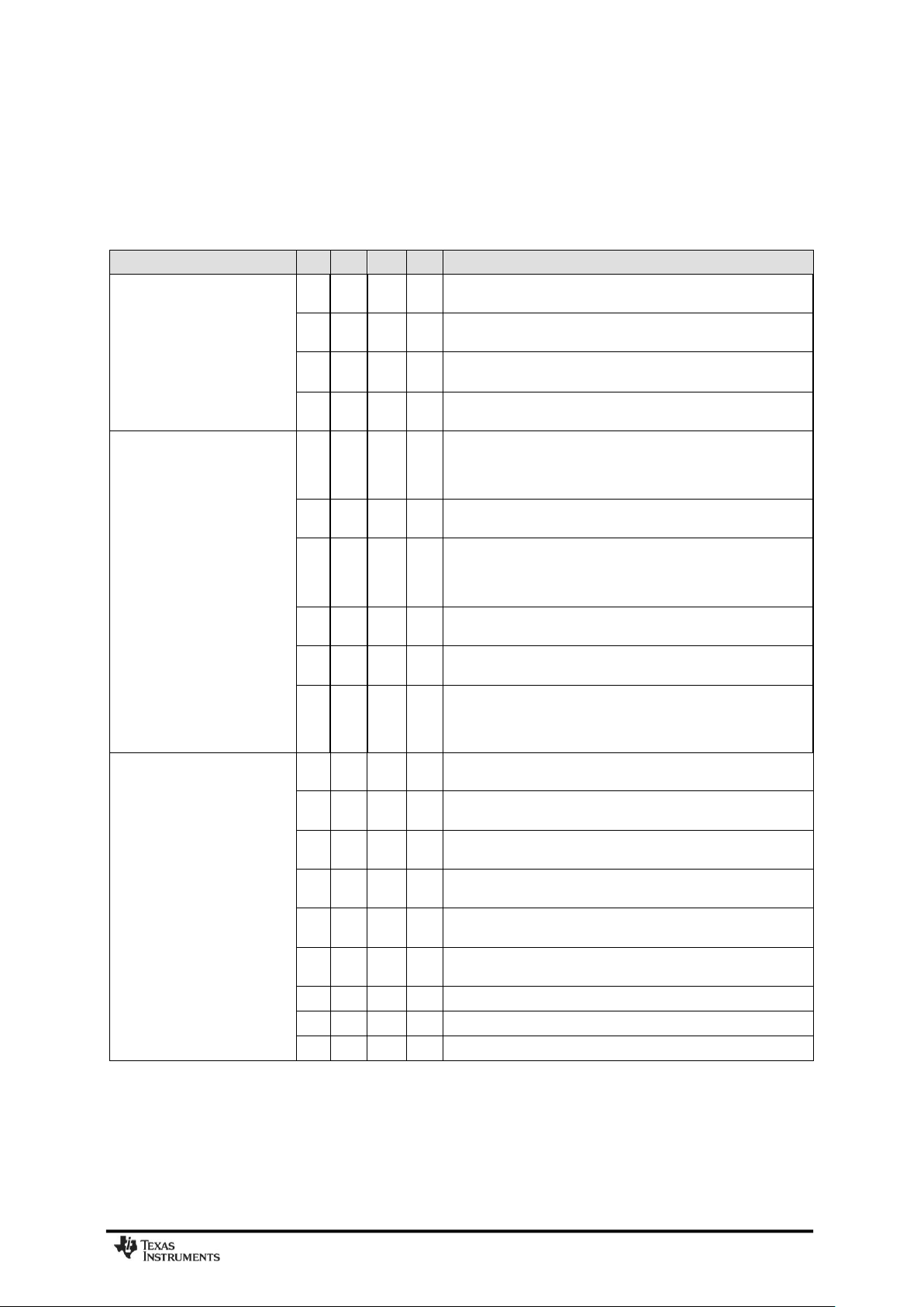
TA = 25C, VDD = 3.0 V if nothing else stated. All measurement results are obtained using the CC1101EM reference designs
([1] and [2]). Reduced current settings (MDMCFG2.DEM_DCFILT_OFF=1) gives a slightly lower current consumption at the cost
of a reduction in sensitivity. See Table 7 for additional details on current consumption and sensitivity.
SWRS061H Page 9 of 98
Page 10
Parameter
Min
Typ
Max
Unit
Condition
Current consumption,
433 MHz
16.0 mA
Receive mode, 1.2 kBaud, register settings optimized for reduced
current, input at sensitivity limit
15.0 mA
Receive mode, 1.2 kBaud, register settings optimized for reduced
current, input well above sensitivity limit
15.7 mA
Receive mode, 38.4 kBaud, register settings optimized for
reduced current, input at sensitivity limit
15.0 mA
Receive mode, 38.4 kBaud, register settings optimized for
reduced current, input well above sensitivity limit
17.1 mA
Receive mode, 250 kBaud, register settings optimized for
reduced current, input at sensitivity limit
15.7 mA
Receive mode, 250 kBaud, register settings optimized for
reduced current, input well above sensitivity limit
29.2 mA
Transmit mode, +10 dBm output power
16.0 mA
Transmit mode, 0 dBm output power
13.1 mA
Transmit mode, –6 dBm output power
Current consumption,
868/915 MHz
15.7 mA
Receive mode, 1.2 kBaud, register settings optimized for
reduced current, input at sensitivity limit.
See Figure 3 for current consumption with register settings
optimized for sensitivity.
14.7 mA
Receive mode, 1.2 kBaud, register settings optimized for
reduced current, input well above sensitivity limit.
See Figure 3 for current consumption with register settings
optimized for sensitivity.
15.6 mA
Receive mode, 38.4 kBaud, register settings optimized for
reduced current, input at sensitivity limit.
See Figure 3 for current consumption with register settings
optimized for sensitivity.
14.6 mA
Receive mode, 38.4 kBaud, register settings optimized for
reduced current, input well above sensitivity limit.
See Figure 3 for current consumption with register settings
optimized for sensitivity.
16.9 mA
Receive mode, 250 kBaud, register settings optimized for
reduced current, input at sensitivity limit.
See Figure 3 for current consumption with register settings
optimized for sensitivity.
15.6 mA
Receive mode, 250 kBaud, register settings optimized for
reduced current, input well above sensitivity limit.
See Figure 3 for current consumption with register settings
optimized for sensitivity.
34.2 mA
Transmit mode, +12 dBm output power, 868 MHz
30.0 mA
Transmit mode, +10 dBm output power, 868 MHz
16.8 mA
Transmit mode, 0 dBm output power, 868 MHz
16.4 mA
Transmit mode, –6 dBm output power, 868 MHz.
33.4 mA
Transmit mode, +11 dBm output power, 915 MHz
30.7 mA
Transmit mode, +10 dBm output power, 915 MHz
17.2 mA
Transmit mode, 0 dBm output power, 915 MHz
17.0 mA
Transmit mode, –6 dBm output power, 915 MHz
CC1101
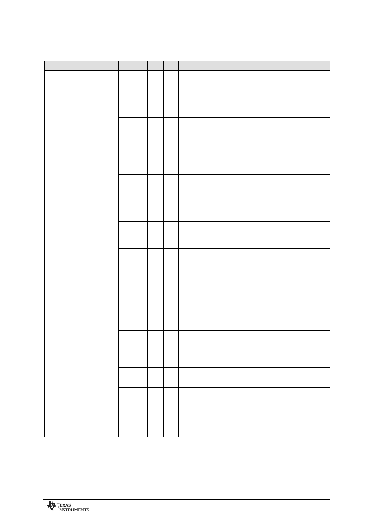
Table 4: Current Consumption
SWRS061H Page 10 of 98
Page 11

16,2
16,4
16,6
16,8
17
17,2
17,4
17,6
17,8
-110 -90 -70 -50 -30 -10
Input Power Level [dBm]
Current [mA]
-40C
+25C
+85C
16,2
16,4
16,6
16,8
17,0
17,2
17,4
17,6
17,8
-100 -80 -60 -40 -20
Input Power Level [dBm]
Current [mA]
-40C
+25C
+85C
16,5
17
17,5
18
18,5
19
19,5
-100 -80 -60 -40 -20
Input Power Level [dBm]
Current [mA]
-40C
+25C
+85C
17,0
17,5
18,0
18,5
19,0
19,5
-90 -70 -50 -30 -10
Input Power Level [dBm]
Current [mA]
-40C
+25C
+85C
Supply Voltage
VDD = 1.8 V
Supply Voltage
VDD = 3.0 V
Supply Voltage
VDD = 3.6 V
Temperature [°C]
-40
25
85
-40
25
85
-40
25
85
Current [mA], PATABLE=0xC0,
+12 dBm
32.7
31.5
30.5
35.3
34.2
33.3
35.5
34.4
33.5
Current [mA], PATABLE=0xC5,
+10 dBm
30.1
29.2
28.3
30.9
30.0
29.4
31.1
30.3
29.6
Current [mA], PATABLE=0x50,
0 dBm
16.4
16.0
15.6
17.3
16.8
16.4
17.6
17.1
16.7
Supply Voltage
VDD = 1.8 V
Supply Voltage
VDD = 3.0 V
Supply Voltage
VDD = 3.6 V
Temperature [°C]
-40
25
85
-40
25
85
-40
25
85
Current [mA], PATABLE=0xC0,
+11 dBm
31.9
30.7
29.8
34.6
33.4
32.5
34.8
33.6
32.7
Current [mA], PATABLE=0xC3,
+10 dBm
30.9
29.8
28.9
31.7
30.7
30.0
31.9
31.0
30.2
Current [mA], PATABLE=0x8E,
0 dBm
17.2
16.8
16.4
17.6
17.2
16.9
17.8
17.4
17.1
Table 5: Typical TX Current Consumption over Temperature and Supply Voltage, 868 MHz
Table 6: Typical TX Current Consumption over Temperature and Supply Voltage, 915 MHz
CC1101
1.2 kBaud GFSK
38.4 kBaud GFSK
250 kBaud GFSK
500 kBaud MSK
Figure 3: Typical RX Current Consumption over Temperature and Input Power Level,
868/915 MHz, Sensitivity Optimized Setting
SWRS061H Page 11 of 98
Page 12

Parameter
Min
Typ
Max
Unit
Condition/Note
Digital channel filter
bandwidth
58 812
kHz
User programmable. The bandwidth limits are proportional to
crystal frequency (given values assume a 26.0 MHz crystal)
Spurious emissions
-68
-66
–57
–47
dBm
dBm
25 MHz – 1 GHz
(Maximum figure is the ETSI EN 300 220 limit)
Above 1 GHz
(Maximum figure is the ETSI EN 300 220 limit)
Typical radiated spurious emission is -49 dBm measured at the
VCO frequency
RX latency
9
bit
Serial operation. Time from start of reception until data is
available on the receiver data output pin is equal to 9 bit
315 MHz
1.2 kBaud data rate, sensitivity optimized, MDMCFG2.DEM_DCFILT_OFF=0
(2-FSK, 1% packet error rate, 20 bytes packet length, 5.2 kHz deviation, 58 kHz digital channel filter bandwidth)
Receiver sensitivity
-111 dBm
Sensitivity can be traded for current consumption by setting
MDMCFG2.DEM_DCFILT_OFF=1. The typical current
consumption is then reduced from 17.2 mA to 15.4 mA at the
sensitivity limit. The sensitivity is typically reduced to -109 dBm
500 kBaud data rate, sensitivity optimized, MDMCFG2.DEM_DCFILT_OFF=0
(MSK, 1% packet error rate, 20 bytes packet length, 812 kHz digital channel filter bandwidth)
Receiver sensitivity
-88 dBm
MDMCFG2.DEM_DCFILT_OFF=1 cannot be used for data rates >
250 kBaud
433 MHz
0.6 kBaud data rate, sensitivity optimized, MDMCFG2.DEM_DCFILT_OFF=0
(GFSK, 1% packet error rate, 20 bytes packet length, 14.3 kHz deviation, 58 kHz digital channel filter bandwidth)
Receiver sensitivity
-116 dBm
1.2 kBaud data rate, sensitivity optimized, MDMCFG2.DEM_DCFILT_OFF=0
(GFSK, 1% packet error rate, 20 bytes packet length, 5.2 kHz deviation, 58 kHz digital channel filter bandwidth)
Receiver sensitivity
-112 dBm
Sensitivity can be traded for current consumption by setting
MDMCFG2.DEM_DCFILT_OFF=1. The typical current
consumption is then reduced from 18.0 mA to 16.0 mA at the
sensitivity limit. The sensitivity is typically reduced to -110 dBm
38.4 kBaud data rate, sensitivity optimized, MDMCFG2.DEM_DCFILT_OFF=0
(GFSK, 1% packet error rate, 20 bytes packet length, 20 kHz deviation, 100 kHz digital channel filter bandwidth)
Receiver sensitivity
–104 dBm
250 kBaud data rate, sensitivity optimized, MDMCFG2.DEM_DCFILT_OFF=0
(GFSK, 1% packet error rate, 20 bytes packet length, 127 kHz deviation, 540 kHz digital channel filter bandwidth)
Receiver sensitivity
-95 dBm
868/915 MHz
1.2 kBaud data rate, sensitivity optimized, MDMCFG2.DEM_DCFILT_OFF=0
(GFSK, 1% packet error rate, 20 bytes packet length, 5.2 kHz deviation, 58 kHz digital channel filter bandwidth)
Receiver sensitivity
–112 dBm
Sensitivity can be traded for current consumption by setting
MDMCFG2.DEM_DCFILT_OFF=1. The typical current
consumption is then reduced from 17.7 mA to 15.7 mA at
sensitivity limit. The sensitivity is typically reduced to -109 dBm
Saturation
–14 dBm
FIFOTHR.CLOSE_IN_RX=0. See more in DN010 [8]
Adjacent channel
rejection
±100 kHz offset
37
dB
Desired channel 3 dB above the sensitivity limit.
100 kHz channel spacing
See Figure 4 for selectivity performance at other offset
frequencies
Image channel
rejection
31 dB
IF frequency 152 kHz
Desired channel 3 dB above the sensitivity limit
CC1101
4.2 RF Receive Section
TA = 25C, VDD = 3.0 V if nothing else stated. All measurement results are obtained using the CC1101EM reference designs
([1] and [2]).
SWRS061H Page 12 of 98
Page 13
Parameter
Min
Typ
Max
Unit
Condition/Note
Blocking
±2 MHz offset
±10 MHz offset
-50
-40
dBm
dBm
Desired channel 3 dB above the sensitivity limit
See Figure 4 for blocking performance at other offset
frequencies
38.4 kBaud data rate, sensitivity optimized, MDMCFG2.DEM_DCFILT_OFF=0
(GFSK, 1% packet error rate, 20 bytes packet length, 20 kHz deviation, 100 kHz digital channel filter bandwidth)
Receiver sensitivity
–104
dBm
Sensitivity can be traded for current consumption by setting
MDMCFG2.DEM_DCFILT_OFF=1. The typical current
consumption is then reduced from 17.7 mA to 15.6 mA at the
sensitivity limit. The sensitivity is typically reduced to -102
dBm
Saturation
–16
dBm
FIFOTHR.CLOSE_IN_RX=0. See more in DN010 [8]
Adjacent channel rejection
-200 kHz offset
+200 kHz offset
12
25
dB
dB
Desired channel 3 dB above the sensitivity limit.
200 kHz channel spacing
See Figure 5 for blocking performance at other offset
frequencies
Image channel rejection
23 dB
IF frequency 152 kHz
Desired channel 3 dB above the sensitivity limit
Blocking
±2 MHz offset
±10 MHz offset
-50
-40
dBm
dBm
Desired channel 3 dB above the sensitivity limit
See Figure 5 for blocking performance at other offset
frequencies
250 kBaud data rate, sensitivity optimized, MDMCFG2.DEM_DCFILT_OFF=0
(GFSK, 1% packet error rate, 20 bytes packet length, 127 kHz deviation, 540 kHz digital channel filter bandwidth)
Receiver sensitivity
–95
dBm
Sensitivity can be traded for current consumption by setting
MDMCFG2.DEM_DCFILT_OFF=1. The typical current
consumption is then reduced from 18.9 mA to 16.9 mA at the
sensitivity limit. The sensitivity is typically reduced to -91 dBm
Saturation
–17
dBm
FIFOTHR.CLOSE_IN_RX=0. See more in DN010 [8]
Adjacent channel rejection
25 dB
Desired channel 3 dB above the sensitivity limit.
750 kHz channel spacing
See Figure 6 for blocking performance at other offset
frequencies
Image channel rejection
14 dB
IF frequency 304 kHz
Desired channel 3 dB above the sensitivity limit
Blocking
±2 MHz offset
±10 MHz offset
-50
-40
dBm
dBm
Desired channel 3 dB above the sensitivity limit
See Figure 6 for blocking performance at other offset
frequencies
500 kBaud data rate, sensitivity optimized, MDMCFG2.DEM_DCFILT_OFF=0
(MSK, 1% packet error rate, 20 bytes packet length, 812 kHz digital channel filter bandwidth)
Receiver sensitivity
–90
dBm
MDMCFG2.DEM_DCFILT_OFF=1 cannot be used for data
rates > 250 kBaud
Image channel rejection
1
dB
IF frequency 355 kHz
Desired channel 3 dB above the sensitivity limit
Blocking
±2 MHz offset
±10 MHz offset
-50
-40
dBm
dBm
Desired channel 3 dB above the sensitivity limit
See Figure 7 for blocking performance at other offset
frequencies
4-FSK, 125 kBaud data rate (250 kbps), sensitivity optimized, MDMCFG2.DEM_DCFILT_OFF=0
(1% packet error rate, 20 bytes packet length, 127 kHz deviation, 406 kHz digital channel filter bandwidth)
Receiver sensitivity
-96
dBm
4-FSK, 250 kBaud data rate (500 kbps), sensitivity optimized, MDMCFG2.DEM_DCFILT_OFF=0
(1% packet error rate, 20 bytes packet length, 254 kHz deviation, 812 kHz digital channel filter bandwidth)
Receiver sensitivity
-91
dBm
4-FSK, 300 kBaud data rate (600 kbps), sensitivity optimized, MDMCFG2.DEM_DCFILT_OFF=0
(1% packet error rate, 20 bytes packet length, 228 kHz deviation, 812 kHz digital channel filter bandwidth)
Receiver sensitivity
-89
dBm
CC1101
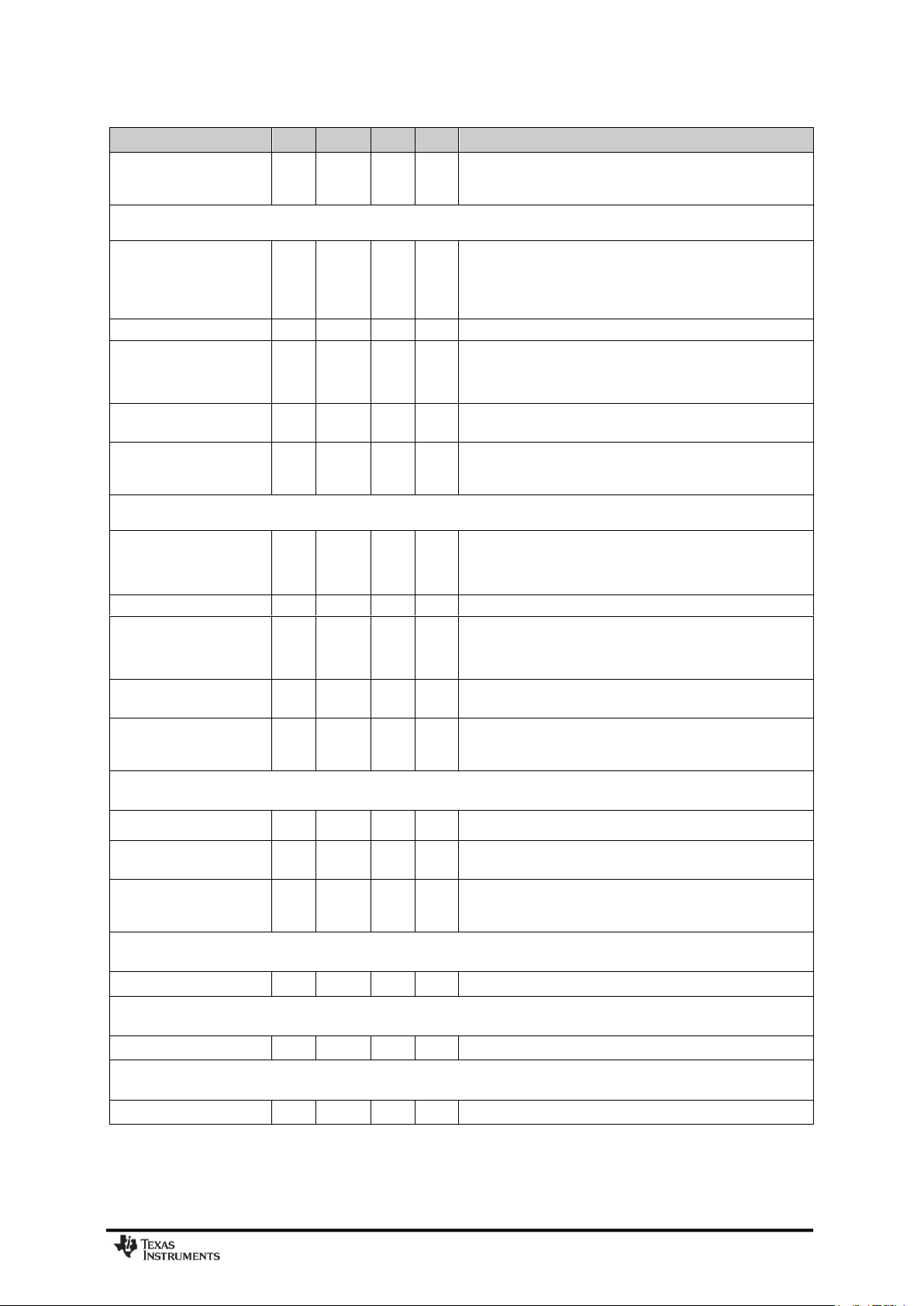
Table 7: RF Receive Section
SWRS061H Page 13 of 98
Page 14
-20
-10
0
10
20
30
40
50
60
70
80
-40 -30 -20 -10 0 10 20 30 40
Offset [MHz]
Blocking [dB]
-10
0
10
20
30
40
50
60
-1 -0,9 -0,8 -0,7 -0,6 -0,5 -0,4 -0,3 -0,2 -0,1 0 0,1 0,2 0,3 0,4 0,5 0,6 0,7 0,8 0,9 1
Offset [MHz]
Selectivity [dB]
Supply Voltage
VDD = 1.8 V
Supply Voltage
VDD = 3.0 V
Supply Voltage
VDD = 3.6 V
Temperature [°C]
-40
25
85
-40
25
85
-40
25
85
Sensitivity [dBm]
1.2 kBaud
-113
-112
-110
-113
-112
-110
-113
-112
-110
Sensitivity [dBm]
38.4 kBaud
-105
-104
-102
-105
-104
-102
-105
-104
-102
Sensitivity [dBm]
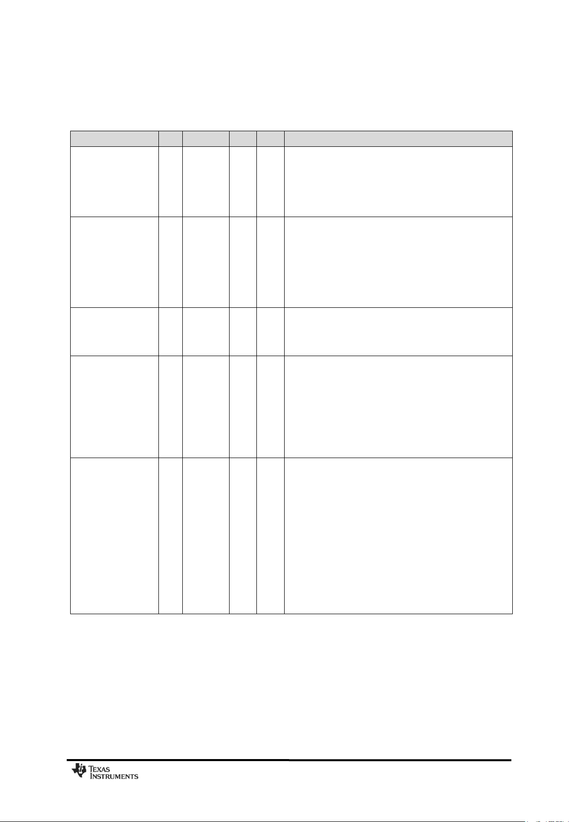
250 kBaud
-97
-96
-92
-97
-95
-92
-97
-94
-92
Sensitivity [dBm]
500 kBaud
-91
-90
-86
-91
-90
-86
-91
-90
-86
Supply Voltage
VDD = 1.8 V
Supply Voltage
VDD = 3.0 V
Supply Voltage
VDD = 3.6 V
Temperature [°C]
-40
25
85
-40
25
85
-40
25
85
Sensitivity [dBm]
1.2 kBaud
-113
-112
-110
-113
-112
-110
-113
-112
-110
Sensitivity [dBm]
38.4 kBaud
-105
-104
-102
-104
-104
-102
-105
-104
-102
Sensitivity [dBm]
250 kBaud
-97
-94
-92
-97
-95
-92
-97
-95
-92
Sensitivity [dBm]
500 kBaud
-91
-89
-86
-91
-90
-86
-91
-89
-86
CC1101
Table 8: Typical Sensitivity over Temperature and Supply Voltage, 868 MHz, Sensitivity Optimized
Setting
Table 9: Typical Sensitivity over Temperature and Supply Voltage, 915 MHz, Sensitivity Optimized
Setting
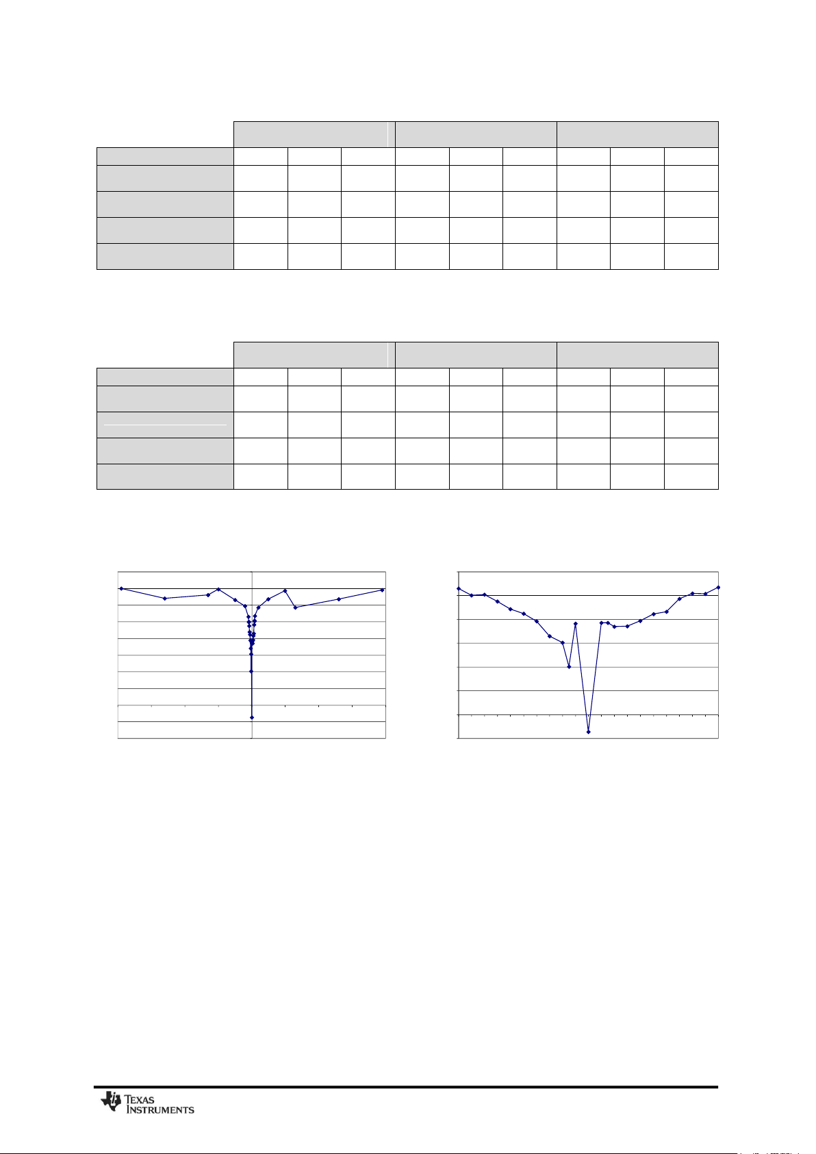
Figure 4: Typical Selectivity at 1.2 kBaud Data Rate, 868.3 MHz, GFSK, 5.2 kHz Deviation. IF
Frequency is 152.3 kHz and the Digital Channel Filter Bandwidth is 58 kHz
SWRS061H Page 14 of 98
Page 15

-20
-10
0
10
20
30
40
50
60
70
-40 -30 -20 -10 0 10 20 30 40
Offset [MHz]
Blocking [dB]
-20
-10
0
10
20
30
40
50
-1 -0,9 -0,8 -0,7 -0,6 -0,5 -0,4 -0,3 -0,2 -0,1 0 0,1 0,2 0,3 0,4 0,5 0,6 0,7 0,8 0,9 1
Offset [MHz]
Selectivity [dB]
-20
-10
0
10
20
30
40
50
60
-40 -30 -20 -10 0 10 20 30 40
Offset [MHz]
Blocking [dB]
-20
-10
0
10
20
30
40
50
-2 -1,5 -1 -0,5 0 0,5 1 1,5 2
Offset [MHz]
Selectivity [dB]
-30
-20
-10
0
10
20
30
40
50
60
-40 -30 -20 -10 0 10 20 30 40
Offset [MHz]
Blocking [dB]
-20
-10
0
10
20
30
40
-2 -1,5 -1 -0,5 0 0,5 1 1,5 2
Offset [MHz]
Selectivity [dB]
CC1101
Figure 5: Typical Selectivity at 38.4 kBaud Data Rate, 868 MHz, GFSK, 20 kHz Deviation. IF
Frequency is 152.3 kHz and the Digital Channel Filter Bandwidth is 100 kHz
Figure 6: Typical Selectivity at 250 kBaud Data Rate, 868 MHz, GFSK, IF Frequency is 304 kHz and
the Digital Channel Filter Bandwidth is 540 kHz
Figure 7: Typical Selectivity at 500 kBaud Data Rate, 868 MHz, GFSK, IF Frequency is 355 kHz and
SWRS061H Page 15 of 98
the Digital Channel Filter Bandwidth is 812 kHz
Page 16
Parameter
Min
Typ
Max
Unit
Condition/Note
Differential load
impedance
315 MHz
433 MHz
868/915 MHz
122 + j31
116 + j41
86.5 + j43
Differential impedance as seen from the RF-port (RF_P and
RF_N) towards the antenna. Follow the CC1101EM reference
designs ([1] and [2]) available from the TI website
Output power,
highest setting
315 MHz
433 MHz
868 MHz
915 MHz
+10
+10
+12
+11
dBm
dBm
dBm
dBm
Output power is programmable, and full range is available in all
frequency bands. Output power may be restricted by
regulatory limits.
See Design Note DN013 [15] for output power and harmonics
figures when using multi-layer inductors. The output power is
then typically +10 dBm when operating at 868/915 MHz.
Delivered to a 50 single-ended load via CC1101EM
reference designs ([1] and [2]) RF matching network
Output power, lowest
setting
-30
dBm
Output power is programmable, and full range is available in all
frequency bands
Delivered to a 50 single-ended load via CC1101EM
reference designs ([1] and [2]) RF matching network
Harmonics, radiated
2
nd
Harm, 433 MHz
3rd Harm, 433 MHz
2
nd
Harm, 868 MHz
3rd Harm, 868 MHz
2
nd
Harm, 915 MHz
3rd Harm, 915 MHz
-49
-40
-47
-55
-50
-54
dBm
dBm
dBm
dBm
dBm
dBm
Measured on CC1101EM reference designs ([1] and [2]) with
CW, maximum output power
The antennas used during the radiated measurements
(SMAFF-433 from R.W. Badland and Nearson S331 868/915)
play a part in attenuating the harmonics
Note: All harmonics are below -41.2 dBm when operating in
the 902 – 928 MHz band
Harmonics, conducted
315 MHz
433 MHz
868 MHz
2
nd
Harm
other harmonics
915 MHz
2
nd
Harm
other harmonics
< -35
< -53
-43
< -45
-36
< -46
-34
< -50
dBm
dBm
dBm
dBm
dBm
dBm
dBm
dBm
Measured with +10 dBm CW at 315 MHz and 433 MHz
Frequencies below 960 MHz
Frequencies above 960 MHz
Frequencies below 1 GHz
Frequencies above 1 GHz
Measured with +12 dBm CW at 868 MHz
Measured with +11 dBm CW at 915 MHz (requirement is -20
dBc under FCC 15.247)
CC1101
4.3 RF Transmit Section
TA = 25C, VDD = 3.0 V, +10 dBm if nothing else stated. All measurement results are obtained using the CC1101EM reference
designs ([1] and [2]).
SWRS061H Page 16 of 98
Page 17
Parameter
Min
Typ
Max
Unit
Condition/Note
Spurious emissions
conducted, harmonics
not included
315 MHz
433 MHz
868 MHz
915 MHz
< -58
< -53
< -50
< -54
< -56
< -50
< -52
< -53
< -51
< -54
dBm
dBm
dBm
dBm
dBm
dBm
dBm
dBm
dBm
dBm
Measured with +10 dBm CW at 315 MHz and 433 MHz
Frequencies below 960 MHz
Frequencies above 960 MHz
Frequencies below 1 GHz
Frequencies above 1 GHz
Frequencies within 47-74, 87.5-118, 174-230, 470-862 MHz
Measured with +12 dBm CW at 868 MHz
Frequencies below 1 GHz
Frequencies above 1 GHz
Frequencies within 47-74, 87.5-118, 174-230, 470-862 MHz
All radiated spurious emissions are within the limits of ETSI.
The peak conducted spurious emission is -53 dBm at 699 MHz
(868 MHz – 169 MHz), which is in a frequency band limited to
-54 dBm by EN 300 220. An alternative filter can be used to
reduce the emission at 699 MHz below -54 dBm, for conducted
measurements, and is shown in Figure 11. See more
information in DN017 [9].
For compliance with modulation bandwidth requirements under
EN 300 220 in the 863 to 870 MHz frequency range it is
recommended to use a 26 MHz crystal for frequencies below
869 MHz and a 27 MHz crystal for frequencies above 869
MHz.
Measured with +11 dBm CW at 915 MHz
Frequencies below 960 MHz
Frequencies above 960 MHz
TX latency
8
bit
Serial operation. Time from sampling the data on the
transmitter data input pin until it is observed on the RF output
ports
Supply Voltage
VDD = 1.8 V
Supply Voltage
VDD = 3.0 V
Supply Voltage
VDD = 3.6 V
Temperature [°C]
-40
25
85
-40
25
85
-40
25
85
Output Power [dBm],
PATABLE=0xC0, +12 dBm
12
11
10
12
12
11
12
12
11
Output Power [dBm],
PATABLE=0xC5, +10 dBm
11
10 9 11
10
10
11
10
10
Output Power [dBm],
PATABLE=0x50, 0 dBm
1 0 -1 2 1 0 2 1 0
Supply Voltage
VDD = 1.8 V
Supply Voltage
VDD = 3.0 V
Supply Voltage
VDD = 3.6 V
Temperature [°C]
-40
25
85
-40
25
85
-40
25
85
Output Power [dBm],
PATABLE=0xC0, +11 dBm
11
10
10
12
11
11
12
11
11
Output Power [dBm],
PATABLE=0x8E, +0 dBm
2 1 0 2 1 0 2 1 0
CC1101
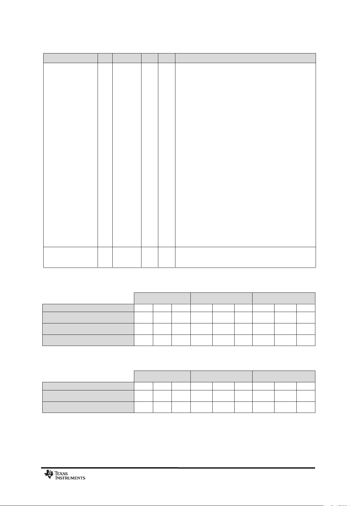
Table 10: RF Transmit Section
Table 11: Typical Variation in Output Power over Temperature and Supply Voltage, 868 MHz
Table 12: Typical Variation in Output Power over Temperature and Supply Voltage, 915 MHz
SWRS061H Page 17 of 98
Page 18
Parameter
Min
Typ
Max
Unit
Condition/Note
Crystal frequency
26
26
27
MHz
For compliance with modulation bandwidth requirements under
EN 300 220 in the 863 to 870 MHz frequency range it is
recommended to use a 26 MHz crystal for frequencies below
869 MHz and a 27 MHz crystal for frequencies above 869 MHz.
Tolerance
±40 ppm
This is the total tolerance including a) initial tolerance, b) crystal
loading, c) aging, and d) temperature dependence. The
acceptable crystal tolerance depends on RF frequency and
channel spacing / bandwidth.
Load capacitance
10
13
20
pF
Simulated over operating conditions
ESR
100
Start-up time
150 µs
This parameter is to a large degree crystal dependent. Measured
on the CC1101EM reference designs ([1] and [2]) using crystal
AT-41CD2 from NDK
Parameter
Min
Typ
Max
Unit
Condition/Note
Calibrated frequency
34.7
34.7
36
kHz
Calibrated RC Oscillator frequency is XTAL
frequency divided by 750
Frequency accuracy after
calibration
±1 %
Temperature coefficient
+0.5
% / C
Frequency drift when temperature changes after
calibration
Supply voltage coefficient
+3 % / V
Frequency drift when supply voltage changes after
calibration
Initial calibration time
2
ms
When the RC Oscillator is enabled, calibration is
continuously done in the background as long as
the crystal oscillator is running
CC1101
4.4 Crystal Oscillator
TA = 25C, VDD = 3.0 V if nothing else is stated. All measurement results obtained using the CC1101EM reference designs ([1]
and [2]).
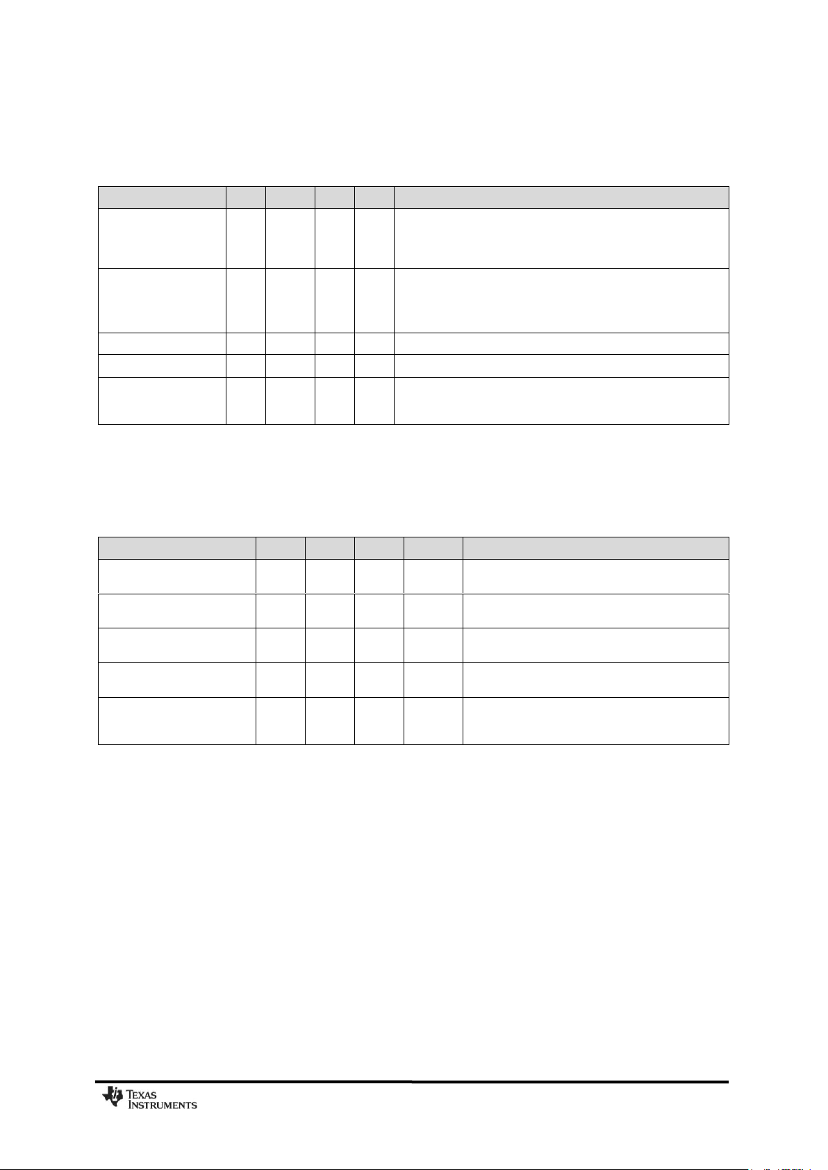
Table 13: Crystal Oscillator Parameters
4.5 Low Power RC Oscillator
TA = 25C, VDD = 3.0 V if nothing else is stated. All measurement results obtained using the CC1101EM reference designs ([1]
and [2]).
Table 14: RC Oscillator Parameters
SWRS061H Page 18 of 98
Page 19

Parameter
Min
Typ
Max
Unit
Condition/Note
Programmed frequency
resolution
397
F
XOSC
/
216
412
Hz
26-27 MHz crystal. The resolution (in Hz) is equal
for all frequency bands
Synthesizer frequency
tolerance
±40 ppm
Given by crystal used. Required accuracy
(including temperature and aging) depends on
frequency band and channel bandwidth / spacing
RF carrier phase noise
–92 dBc/Hz
@ 50 kHz offset from carrier
RF carrier phase noise
–92 dBc/Hz
@ 100 kHz offset from carrier
RF carrier phase noise
–92 dBc/Hz
@ 200 kHz offset from carrier
RF carrier phase noise
–98 dBc/Hz
@ 500 kHz offset from carrier
RF carrier phase noise
–107
dBc/Hz
@ 1 MHz offset from carrier
RF carrier phase noise
–113
dBc/Hz
@ 2 MHz offset from carrier
RF carrier phase noise
–119
dBc/Hz
@ 5 MHz offset from carrier
RF carrier phase noise
–129
dBc/Hz
@ 10 MHz offset from carrier
PLL turn-on / hop time
( See Table 34)
72
75
75
s
Time from leaving the IDLE state until arriving in
the RX, FSTXON or TX state, when not
performing calibration. Crystal oscillator running.
PLL RX/TX settling time
( See Table 34)
29
30
30
s
Settling time for the 1·IF frequency step from RX
to TX
PLL TX/RX settling time
( See Table 34)
30
31
31
s
Settling time for the 1·IF frequency step from TX
to RX. 250 kbps data rate.
PLL calibration time
(See Table 35)
685
712
724
s
Calibration can be initiated manually or
automatically before entering or after leaving
RX/TX
Parameter
Min
Typ
Max
Unit
Condition/Note
Output voltage at –40C
0.651 V
Output voltage at 0C
0.747 V
Output voltage at +40C
0.847 V
Output voltage at +80C
0.945 V Temperature coefficient
2.47
mV/C
Fitted from –20 C to +80 C
Error in calculated
temperature, calibrated
-2
*
0
2
*
C
From –20 C to +80 C when using 2.47 mV / C, after
1-point calibration at room temperature
*
The indicated minimum and maximum error with 1point calibration is based on simulated values for
typical process parameters
Current consumption
increase when enabled
0.3 mA
CC1101
4.6 Frequency Synthesizer Characteristics
TA = 25C, VDD = 3.0 V if nothing else is stated. All measurement results are obtained using the CC1101EM reference designs
([1] and [2]). Min figures are given using a 27 MHz crystal. Typ and max figures are given using a 26 MHz crystal.
Table 15: Frequency Synthesizer Parameters
4.7 Analog Temperature Sensor
TA = 25C, VDD = 3.0 V if nothing else is stated. All measurement results obtained using the CC1101EM reference designs ([1]
and [2]). Note that it is necessary to write 0xBF to the PTEST register to use the analog temperature sensor in the IDLE state.
Table 16: Analog Temperature Sensor Parameters
SWRS061H Page 19 of 98
Page 20

1
20 19 18 17 16
15
14
13
12
11
109876
5
4
3
2
GND
Exposed die
attach pad
SCLK
SO (GDO1)
GDO2
DVDD
DCOUPL
GDO0 (ATEST)
XOSC_Q1
AVDD
XOSC_Q2
AVDD
RF_P
RF_N
GND
AVDD
RBIAS
DGUARD
GND
SI
CSn
AVDD
Digital Inputs/Outputs
Min
Max
Unit
Condition
Logic "0" input voltage
0
0.7
V Logic "1" input voltage
VDD-0.7
VDD
V
Logic "0" output voltage
0
0.5
V
For up to 4 mA output current
Logic "1" output voltage
VDD-0.3
VDD
V
For up to 4 mA output current
Logic "0" input current
N/A
–50
nA
Input equals 0V
Logic "1" input current
N/A
50
nA
Input equals VDD
Parameter
Min
Typ
Max
Unit
Condition/Note
Power-up ramp-up time
5
ms
From 0V until reaching 1.8V
Power off time
1
ms
Minimum time between power-on and power-off
Note: The exposed die attach pad must be connected to a solid ground plane as this is the main
ground connection for the chip
CC1101
4.8 DC Characteristics
TA = 25C if nothing else stated.
Table 17: DC Characteristics
4.9 Power-On Reset
For proper Power-On-Reset functionality the power supply should comply with the requirements in
Table 18 below. Otherwise, the chip should be assumed to have unknown state until transmitting an
SRES strobe over the SPI interface. See Section 19.1 on page 50 for further details.
5 Pin Configuration
The
CC1101
configuration.
pin-out is shown in Figure 8 and Table 19. See Section 26 for details on the I/O
Table 18: Power-On Reset Requirements
Figure 8: Pinout Top View
.
SWRS061H Page 20 of 98
Page 21

Pin #
Pin Name
Pin type
Description
1
SCLK
Digital Input
Serial configuration interface, clock input
2
SO (GDO1)
Digital Output
Serial configuration interface, data output
Optional general output pin when CSn is high
3
GDO2
Digital Output
Digital output pin for general use:
Test signals
FIFO status signals
Clear channel indicator
Clock output, down-divided from XOSC
Serial output RX data
4
DVDD
Power (Digital)
1.8 - 3.6 V digital power supply for digital I/O‟s and for the digital core
voltage regulator
5
DCOUPL
Power (Digital)
1.6 - 2.0 V digital power supply output for decoupling
NOTE: This pin is intended for use with the
CC1101
only. It can not be used
to provide supply voltage to other devices
6
GDO0
(ATEST)
Digital I/O
Digital output pin for general use:
Test signals
FIFO status signals
Clear channel indicator
Clock output, down-divided from XOSC
Serial output RX data
Serial input TX data
Also used as analog test I/O for prototype/production testing
7
CSn
Digital Input
Serial configuration interface, chip select
8
XOSC_Q1
Analog I/O
Crystal oscillator pin 1, or external clock input
9
AVDD
Power (Analog)
1.8 - 3.6 V analog power supply connection
10
XOSC_Q2
Analog I/O
Crystal oscillator pin 2
11
AVDD
Power (Analog)
1.8 - 3.6 V analog power supply connection
12
RF_P
RF I/O
Positive RF input signal to LNA in receive mode
Positive RF output signal from PA in transmit mode
13
RF_N
RF I/O
Negative RF input signal to LNA in receive mode
Negative RF output signal from PA in transmit mode
14
AVDD
Power (Analog)
1.8 - 3.6 V analog power supply connection
15
AVDD
Power (Analog)
1.8 - 3.6 V analog power supply connection
16
GND
Ground (Analog)
Analog ground connection
17
RBIAS
Analog I/O
External bias resistor for reference current
18
DGUARD
Power (Digital)
Power supply connection for digital noise isolation
19
GND
Ground (Digital)
Ground connection for digital noise isolation
20
SI
Digital Input
Serial configuration interface, data input
CC1101
Table 19: Pinout Overview
SWRS061H Page 21 of 98
Page 22

BIAS
PA
RBIAS XOSC_Q1 XOSC_Q2
CSn
SI
SO (GDO1)
XOSC
SCLK
LNA
0
90
FREQ
SYNTH
ADC
ADC
DEMODULATOR
FEC / INTERLEAVER
PACKET HANDLER
RXFIFO
MODULATOR
TXFIFO
DIGITAL INTERFACE TO MCU
RADIO CONTROL
RF_P
RF_N
GDO2
GDO0 (ATEST)
RC OSC
6 Circuit Description
CC1101
A simplified block diagram of
Figure 9:
CC1101
CC1101
Simplified Block Diagram
is shown
in Figure 9.
CC1101
features a low-IF receiver. The received
RF signal is amplified by the low-noise
amplifier (LNA) and down-converted in
quadrature (I and Q) to the intermediate
frequency (IF). At IF, the I/Q signals are
digitised by the ADCs. Automatic gain control
(AGC), fine channel filtering, demodulation,
and bit/packet synchronization are performed
digitally.
The transmitter part of
CC1101
is based on
direct synthesis of the RF frequency. The
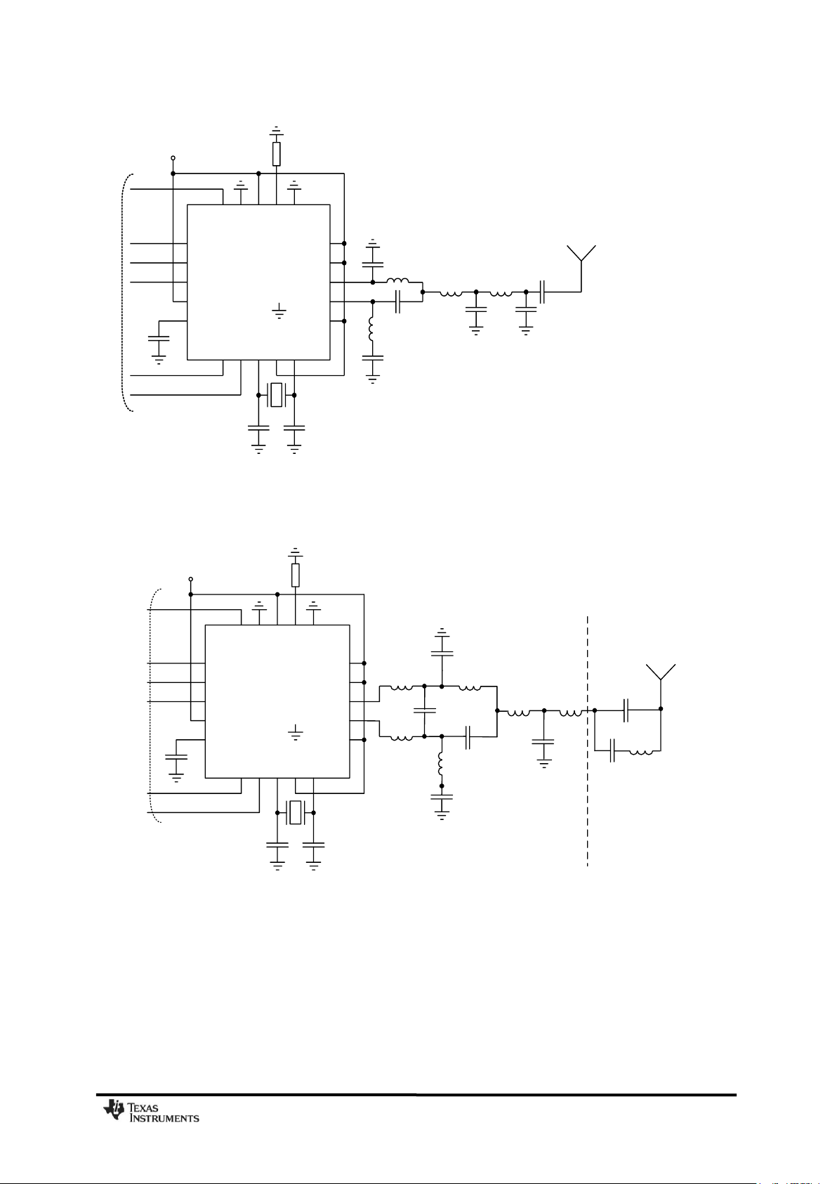
7 Application Circuit
Only a few external components are required
for using the
application circuits for
Figure 10 and
Figure 11. The external components are
described in Table 20, and typical values are
given in Table 21.
The 315 MHz and 433 MHz CC1101EM
reference design [1] use inexpensive multilayer inductors. The 868 MHz and 915 MHz
CC1101EM reference design [2] use wire-
CC1101
. The recommended
CC1101
are shown in
frequency synthesizer includes a completely
on-chip LC VCO and a 90 degree phase
shifter for generating the I and Q LO signals to
the down-conversion mixers in receive mode.
A crystal is to be connected to XOSC_Q1 and
XOSC_Q2. The crystal oscillator generates the
reference frequency for the synthesizer, as
well as clocks for the ADC and the digital part.
A 4-wire SPI serial interface is used for
configuration and data buffer access.
The digital baseband includes support for
channel configuration, packet handling, and
data buffering.
wound inductors as this give better output
power, sensitivity, and attenuation of
harmonics compared to using multi-layer
inductors. Refer to design note DN032 [24] for
information about performance when using
wire-wound inductors from different vendors.
See also Design Note DN013 [15], which gives
the output power and harmonics when using
multi-layer inductors. The output power is then
typically +10 dBm when operating at 868/915
MHz.
7.1 Bias Resistor
The bias resistor R171 is used to set an accurate bias current.
SWRS061H Page 22 of 98
Page 23

parasiticL
C
CC
C
10181
11
1
7.2 Balun and RF Matching
CC1101
The balanced RF input and output of
share two common pins and are designed for
a simple, low-cost matching and balun network
on the printed circuit board. The receive- and
transmit switching at the
controlled by a dedicated on-chip function,
eliminating the need for an external RX/TXswitch.
A few external passive components combined
with the internal RX/TX switch/termination
circuitry ensures match in both RX and TX
mode. The components between the
RF_N/RF_P pins and the point where the two
signals are joined together (C131, C121, L121
and L131 for the 315/433 MHz reference
design [1], and L121, L131, C121, L122,
C131, C122 and L132 for the 868/915 MHz
reference design [2]) form a balun that
converts the differential RF signal on
a single-ended RF signal. C124 is needed for
7.3 Crystal
A crystal in the frequency range 26-27 MHz
must be connected between the XOSC_Q1
and XOSC_Q2 pins. The oscillator is designed
for parallel mode operation of the crystal. In
addition, loading capacitors (C81 and C101)
for the crystal are required. The loading
capacitor values depend on the total load
capacitance, CL, specified for the crystal. The
total load capacitance seen between the
crystal terminals should equal CL for the
crystal to oscillate at the specified frequency.
CC1101
CC1101
front-end is
CC1101
to
DC blocking. Together with an appropriate LC
network, the balun components also transform
the impedance to match a 50 load. C125
provides DC blocking and is only needed if
there is a DC path in the antenna. For the
868/915 MHz reference design, this
component may also be used for additional
filtering, see Section 7.5 below.
Suggested values for 315 MHz, 433 MHz, and
868/915 MHz are listed in Table 21.
The balun and LC filter component values and
their placement are important to keep the
performance optimized. It is highly
recommended to follow the CC1101EM
reference design ([1] and [2]). Gerber files and
schematics for the reference designs are
available for download from the TI website.
swing. This ensures a fast start-up, and keeps
the drive level to a minimum. The ESR of the
crystal should be within the specification in
order to ensure a reliable start-up (see Section
4.4).
The initial tolerance, temperature drift, aging
and load pulling should be carefully specified
in order to meet the required frequency
accuracy in a certain application.
Avoid routing digital signals with sharp edges
close to XOSC_Q1 PCB track or underneath
the crystal Q1 pad as this may shift the crystal
dc operating point and result in duty cycle
variation.
The parasitic capacitance is constituted by pin
input capacitance and PCB stray capacitance.
Total parasitic capacitance is typically 2.5 pF.
The crystal oscillator is amplitude regulated.
This means that a high current is used to start
up the oscillations. When the amplitude builds
up, the current is reduced to what is necessary
to maintain approximately 0.4 Vpp signal
7.4 Reference Signal
The chip can alternatively be operated with a
reference signal from 26 to 27 MHz instead of
a crystal. This input clock can either be a fullswing digital signal (0 V to VDD) or a sine
wave of maximum 1 V peak-peak amplitude.
The reference signal must be connected to the
SWRS061H Page 23 of 98
For compliance with modulation bandwidth
requirements under EN 300 220 in the 863 to
870 MHz frequency range it is recommended
to use a 26 MHz crystal for frequencies below
869 MHz and a 27 MHz crystal for frequencies
above 869 MHz.
XOSC_Q1 input. The sine wave must be
connected to XOSC_Q1 using a serial
capacitor. When using a full-swing digital
signal, this capacitor can be omitted. The
XOSC_Q2 line must be left un-connected. C81
Page 24
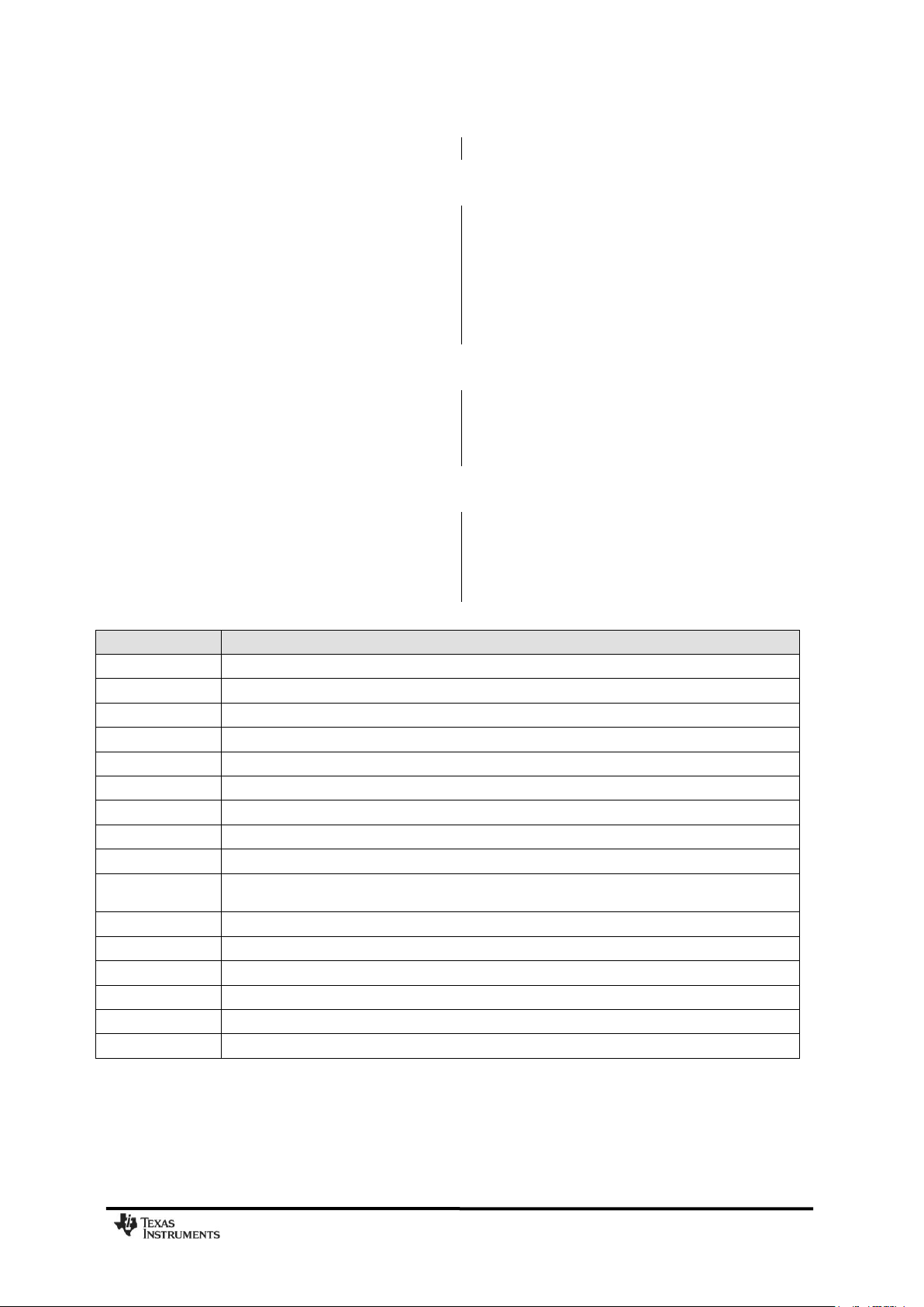
Component
Description
C51
Decoupling capacitor for on-chip voltage regulator to digital part
C81/C101
Crystal loading capacitors
C121/C131
RF balun/matching capacitors
C122
RF LC filter/matching filter capacitor (315/433 MHz). RF balun/matching capacitor (868/915 MHz).
C123
RF LC filter/matching capacitor
C124
RF balun DC blocking capacitor
C125
RF LC filter DC blocking capacitor and part of optional RF LC filter (868/915 MHz)
C126
Part of optional RF LC filter and DC-block (868/915 MHz)
L121/L131
RF balun/matching inductors (inexpensive multi-layer type)
L122
RF LC filter/matching filter inductor (315 and 433 MHz). RF balun/matching inductor (868/915 MHz).
(inexpensive multi-layer type)
L123
RF LC filter/matching filter inductor (inexpensive multi-layer type)
L124
RF LC filter/matching filter inductor (inexpensive multi-layer type)
L125
Optional RF LC filter/matching filter inductor (inexpensive multi-layer type) (868/915 MHz)
L132
RF balun/matching inductor. (inexpensive multi-layer type)
R171
Resistor for internal bias current reference
XTAL
26 – 27 MHz crystal
and C101 can be omitted when using a reference signal.
7.5 Additional Filtering
CC1101
In the 868/915 MHz reference design, C126
and L125 together with C125 build an optional
filter to reduce emission at carrier frequency –
169 MHz. This filter is necessary for
applications with an external antenna
connector that seek compliance with ETSI EN
300-220. For more information, see DN017 [9].
7.6 Power Supply Decoupling
The power supply must be properly decoupled
close to the supply pins. Note that decoupling
capacitors are not shown in the application
circuit. The placement and the size of the
7.7 Antenna Considerations
The reference design ([1] and [2]) contains a
SMA connector and is matched for a 50
load. The SMA connector makes it easy to
connect evaluation modules and prototypes to
different test equipment for example a
If this filtering is not necessary, C125 will work
as a DC block (only necessary if there is a DC
path in the antenna). C126 and L125 should in
that case be left unmounted.
Additional external components (e.g. an RF
SAW filter) may be used in order to improve
the performance in specific applications.
decoupling capacitors are very important to
achieve the optimum performance. The
CC1101EM reference designs ([1] and [2])
should be followed closely.
spectrum analyzer. The SMA connector can
also be replaced by an antenna suitable for
the desired application. Please refer to the
antenna selection guide [13] for further details
regarding antenna solutions provided by TI.
Table 20: Overview of External Components (excluding supply decoupling capacitors)
SWRS061H Page 24 of 98
Page 25
Antenna
(50 Ohm)
Digital Inteface
1.8V-3.6V power supply
6 GDO0
7 CSn
8 XOSC_Q1
9 AVDD
10 XOSC_Q2
SI 20
GND 19
DGUARD 18
RBIAS 17
GND 16
1 SCLK
2 SO
(GDO1)
3 GDO2
4 DVDD
5 DCOUPL
AVDD 15
AVDD 14
RF_N 13
RF_P 12
AVDD 11
XTAL
L122 L123
C122 C123
C125
R171
C81 C101
C51
CSn
GDO0
(optional)
GDO2
(optional)
SO
(GDO1)
SCLK
SI
CC1101
DIE ATTACH PAD:
C131
C121
L121
L131
C124
Antenna
(50 Ohm)
Digital Interface
1.8V-3.6V power supply
6 GDO0
7 CSn
8 XOSC_Q1
9 AVDD
10 XOSC_Q2
SI 20
GND 19
DGUARD 18
RBIAS 17
GND 16
1 SCLK
2 SO
(GDO1)
3 GDO2
4 DVDD
5 DCOUPL
AVDD 15
AVDD 14
RF_N 13
RF_P 12
AVDD 11
XTAL
C121 C122
L122
L132
C131
L121
L123
C125
R171
C81 C101
C51
CSn
GDO0
(optional)
GDO2
(optional)
SO
(GDO1)
SCLK
SI
CC1101
DIE ATTACH PAD:
L131
C124
C123
L124
C126 L125
C126 and L125
may be added to
build an optional
filter to reduce
emission at 699
MHz
Figure 10: Typical Application and Evaluation Circuit 315/433 MHz (excluding supply
decoupling capacitors)
CC1101
Figure 11: Typical Application and Evaluation Circuit 868/915 MHz (excluding supply
decoupling capacitors)
SWRS061H Page 25 of 98
Page 26

1
Component
Value at 315MHz
Value at 433MHz
Value at
868/915MHz
Manufacturer
C51
100 nF ± 10%, 0402 X5R
Murata GRM1555C series
C81
27 pF ± 5%, 0402 NP0
Murata GRM1555C series
C101
27 pF ± 5%, 0402 NP0
Murata GRM1555C series
C121
6.8 pF ± 0.5 pF,
0402 NP0
3.9 pF ± 0.25 pF,
0402 NP0
1.0 pF ± 0.25 pF,
0402 NP0
Murata GRM1555C series
C122
12 pF ± 5%, 0402
NP0
8.2 pF ± 0.5 pF,
0402 NP0
1.5 pF ± 0.25 pF,
0402 NP0
Murata GRM1555C series
C123
6.8 pF ± 0.5 pF,
0402 NP0
5.6 pF ± 0.5 pF,
0402 NP0
3.3 pF ± 0.25 pF,
0402 NP0
Murata GRM1555C series
C124
220 pF ± 5%,
0402 NP0
220 pF ± 5%, 0402
NP0
100 pF ± 5%, 0402
NP0
Murata GRM1555C series
C125
220 pF ± 5%,
0402 NP0
220 pF ± 5%, 0402
NP0
12 pF ± 5%, 0402
NP0
Murata GRM1555C series
C126
47 pF ± 5%, 0402
NP0
Murata GRM1555C series
C131
6.8 pF ± 0.5 pF,
0402 NP0
3.9 pF ± 0.25 pF,
0402 NP0
1.5 pF ± 0.25 pF,
0402 NP0
Murata GRM1555C series
L121
33 nH ± 5%, 0402
monolithic
27 nH ± 5%, 0402
monolithic
12 nH ± 5%, 0402
monolithic
Murata LQG15HS series (315/433 MHz)
Murata LQW15xx series (868/915 MHz)
L122
18 nH ± 5%, 0402
monolithic
22 nH ± 5%, 0402
monolithic
18 nH ± 5%, 0402
monolithic
Murata LQG15HS series (315/433 MHz)
Murata LQW15xx series (868/915 MHz)
L123
33 nH ± 5%, 0402
monolithic
27 nH ± 5%, 0402
monolithic
12 nH ± 5%, 0402
monolithic
Murata LQG15HS series (315/433 MHz)
Murata LQW15xx series (868/915 MHz)
L124
12 nH ± 5%, 0402
monolithic
Murata LQG15HS series (315/433 MHz)
Murata LQW15xx series (868/915 MHz)
L125
3.3 nH ± 5%, 0402
monolithic
Murata LQG15HS series (315/433 MHz)
Murata LQW15xx series (868/915 MHz)
L131
33 nH ± 5%, 0402
monolithic
27 nH ± 5%, 0402
monolithic
12 nH ± 5%, 0402
monolithic
Murata LQG15HS series (315/433 MHz)
Murata LQW15xx series (868/915 MHz)
L132
18 nH ± 5%, 0402
monolithic
Murata LQG15HS series (315/433 MHz)
Murata LQW15xx series (868/915 MHz)
R171
56 kΩ ± 1%, 0402
Koa RK73 series
XTAL
26.0 MHz surface mount crystal
NDK, NX3225GA or AT-41CD2
CC1101
Refer to design note DN032 [24] for information about performance when using inductors from
other vendors than Murata.
7.8 PCB Layout Recommendations
The top layer should be used for signal
routing, and the open areas should be filled
with metallization connected to ground using
several vias.
The area under the chip is used for grounding
and shall be connected to the bottom ground
plane with several vias for good thermal
performance and sufficiently low inductance to
ground.
Table 21: Bill Of Materials for the Application Circuit1
In the CC1101EM reference designs ([1] and
[2]), 5 vias are placed inside the exposed die
attached pad. These vias should be “tented”
(covered with solder mask) on the component
side of the PCB to avoid migration of solder
through the vias during the solder reflow
process.
The solder paste coverage should not be
100%. If it is, out gassing may occur during the
SWRS061H Page 26 of 98
Page 27
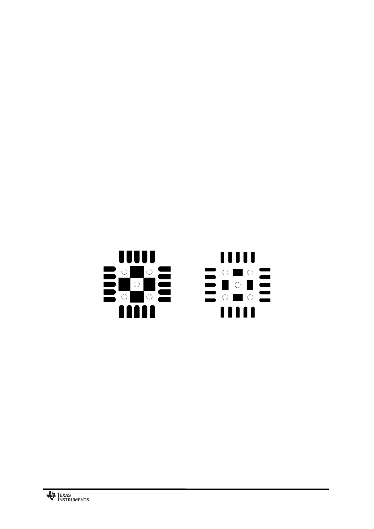
CC1101
reflow process, which may cause defects
(splattering, solder balling). Using “tented” vias
reduces the solder paste coverage below
100%. See Figure 12 for top solder resist and
top paste masks.
Each decoupling capacitor should be placed
as close as possible to the supply pin it is
supposed to decouple. Each decoupling
capacitor should be connected to the power
line (or power plane) by separate vias. The
best routing is from the power line (or power
plane) to the decoupling capacitor and then to
the
CC1101
supply pin. Supply power filtering is
very important.
Each decoupling capacitor ground pad should
be connected to the ground plane by separate
vias. Direct connections between neighboring
power pins will increase noise coupling and
should be avoided unless absolutely
necessary. Routing in the ground plane
underneath the chip or the balun/RF matching
circuit, or between the chip‟s ground vias and
the decoupling capacitor‟s ground vias should
be avoided. This improves the grounding and
ensures the shortest possible current return
path.
Avoid routing digital signals with sharp edges
close to XOSC_Q1 PCB track or underneath
the crystal Q1 pad as this may shift the crystal
dc operating point and result in duty cycle
variation.
The external components should ideally be as
small as possible (0402 is recommended) and
surface mount devices are highly
recommended. Please note that components
with different sizes than those specified may
have differing characteristics.
Precaution should be used when placing the
microcontroller in order to avoid noise
interfering with the RF circuitry.
A CC1101DK Development Kit with a fully
assembled CC1101EM Evaluation Module is
available. It is strongly advised that this
reference layout is followed very closely in
order to get the best performance. The
schematic, BOM and layout Gerber files are all
available from the TI website ([1] and [2]).
Figure 12: Left: Top Solder Resist Mask (Negative). Right: Top Paste Mask. Circles are Vias
8 Configuration Overview
CC1101
performance for many different applications.
Configuration is done using the SPI interface.
See Section 10 below for more description of
the SPI interface. The following key
parameters can be programmed:
Power-down / power up mode
Crystal oscillator power-up / power-down
Receive / transmit mode
RF channel selection
Data rate
Modulation format
RX channel filter bandwidth
RF output power
can be configured to achieve optimum
SWRS061H Page 27 of 98
Data buffering with separate 64-byte
receive and transmit FIFOs
Packet radio hardware support
Forward Error Correction (FEC) with
interleaving
Data whitening
Wake-On-Radio (WOR)
Details of each configuration register can be
found in Section 29, starting on page 66.
Figure 13 shows a simplified state diagram
that explains the main
with typical usage and current consumption.
For detailed information on controlling the
CC1101
states together
Page 28

Transmit mode Receive mode
IDLE
Manual freq.
synth. calibration
RX FIFO
overflow
TX FIFO
underflow
Frequency
synthesizer on
SFSTXON
SRX or wake-on-radio (WOR)
STX
STX
STX or RXOFF_MODE=10
RXOFF_MODE = 00
SFTX
SRX or TXOFF_MODE = 11
SIDLE
SCAL
SFRX
IDLE
TXOFF_MODE = 00
SFSTXON or RXOFF_MODE = 01
SRX or STX or SFSTXON or wake-on-radio (WOR)
Sleep
SPWD or wake-on-radio (WOR)
Crystal
oscillator off
SXOFF
CSn = 0
CSn = 0
TXOFF_MODE = 01
Frequency
synthesizer startup,
optional calibration,
settling
Optional freq.
synth. calibration
Default state when the radio is not
receiving or transmitting. Typ.
current consumption: 1.7 mA.
Lowest power mode. Most
register values are retained.
Current consumption typ
200 nA, or typ 500 nA when
wake-on-radio (WOR) is
enabled.
All register values are
retained. Typ. current
consumption; 165 µA.
Used for calibrating frequency
synthesizer upfront (entering
receive or transmit mode can
then be done quicker).
Transitional state. Typ. current
consumption: 8.4 mA.
Frequency synthesizer is turned on, can optionally be
calibrated, and then settles to the correct frequency.
Transitional state. Typ. current consumption: 8.4 mA.
Frequency synthesizer is on,
ready to start transmitting.
Transmission starts very
quickly after receiving the STX
command strobe.Typ. current
consumption: 8.4 mA.
Typ. current consumption:
16.8 mA at 0 dBm output,
30.0 mA at +10 dBm output,
34.2 mA at +12 dBm output.
Typ. current
consumption:
from 14.7 mA (strong
input signal) to 15.7 mA
(weak input signal).
Optional transitional state. Typ.
current consumption: 8.4 mA.
In FIFO-based modes,
transmission is turned off and
this state entered if the TX
FIFO becomes empty in the
middle of a packet. Typ.
current consumption: 1.7 mA.
In FIFO-based modes,
reception is turned off and this
state entered if the RX FIFO
overflows. Typ. current
consumption: 1.7 mA.
CC1101
CC1101
state machine, and a complete state
diagram, see Section 19, starting on page 50.
Figure 13: Simplified State Diagram, with Typical Current Consumption at 1.2 kBaud Data
Rate and MDMCFG2.DEM_DCFILT_OFF=1 (current optimized). Frequency Band = 868 MHz
SWRS061H Page 28 of 98
Page 29

9 Configuration Software
CC1101
CC1101
can be configured using the SmartRFTM
Studio software [5]. The SmartRF Studio
software is highly recommended for obtaining
optimum register settings, and for evaluating
performance and functionality. A screenshot of
the SmartRF Studio user interface for
shown in Figure 14.
CC1101
is
After chip reset, all the registers have default
values as shown in the tables in Section 29.
The optimum register setting might differ from
the default value. After a reset all registers that
shall be different from the default value
therefore needs to be programmed through
the SPI interface.
Figure 14: SmartRFTM Studio [5] User Interface
10 4-wire Serial Configuration and Data Interface
CC1101
compatible interface (SI, SO, SCLK and CSn)
where
also used to read and write buffered data. All
transfers on the SPI interface are done most
significant bit first.
All transactions on the SPI interface start with
a header byte containing a R/W¯ bit, a burst
access bit (B), and a 6-bit address (A5 – A0).
The CSn pin must be kept low during transfers
on the SPI bus. If CSn goes high during the
is configured via a simple 4-wire SPI-
CC1101
is the slave. This interface is
transfer of a header byte or during read/write
from/to a register, the transfer will be
cancelled. The timing for the address and data
transfer on the SPI interface is shown in Figure
15 with reference to Table 22.
When CSn is pulled low, the MCU must wait
until
CC1101
transfer the header byte. This indicates that
the crystal is running. Unless the chip was in
the SLEEP or XOFF states, the SO pin will
always go low immediately after taking CSn
low.
SO pin goes low before starting to
SWRS061H Page 29 of 98
Page 30
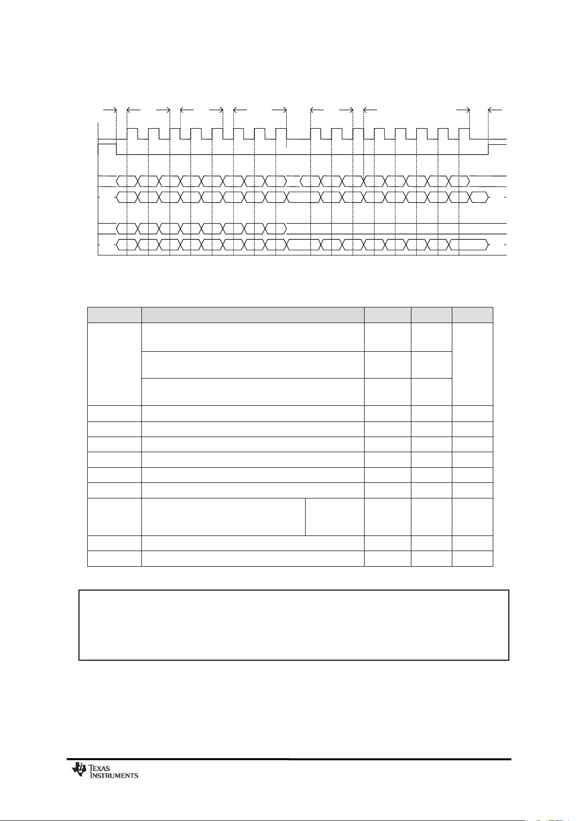
0
A5 A4
A3
A2
A0
A1
DW7
1
Read from register:
Write to register:
Hi-Z
X
SCLK:
CSn:
SI
SO
SI
SO
Hi-Z
t
sp
t
ch
t
cl
t
sd
t
hd
t
ns
X
X
Hi-Z
X
Hi-Z
S7
X
DW6 DW5 D
W
4 DW3 DW2 D
W
1 DW0
B
S5
S4
S3 S2 S1 S0
S7
S6
S5 S4 S3
S2
S1 S0
B
B
A5 A4 A3 A2 A1 A0
S7
B S5 S4 S3 S2 S1 S0
DR7 DR6 D
R
5 DR4 DR3 D
R
2 DR1 DR0
Parameter
Description
Min
Max
Units
f
SCLK
SCLK frequency
100 ns delay inserted between address byte and data byte (single access), or
between address and data, and between each data byte (burst access).
-
10
MHz
SCLK frequency, single access
No delay between address and data byte
- 9 SCLK frequency, burst access
No delay between address and data byte, or between data bytes
-
6.5
t
sp,pd
CSn low to positive edge on SCLK, in power-down mode
150
-
s
tsp
CSn low to positive edge on SCLK, in active mode
20 - ns
tch
Clock high
50 - ns
tcl
Clock low
50 - ns
t
rise
Clock rise time
-
40
ns
t
fall
Clock fall time
-
40
ns
tsd
Setup data (negative SCLK edge) to
positive edge on SCLK
(tsd applies between address and data bytes, and between
data bytes)
Single access
Burst access
55
76 - -
ns
thd
Hold data after positive edge on SCLK
20 - ns
tns
Negative edge on SCLK to CSn high.
20 - ns
Note: The minimum t
sp,pd
figure in Table 22 can be used in cases where the user does not read
the CHIP_RDYn signal. CSn low to positive edge on SCLK when the chip is woken from powerdown depends on the start-up time of the crystal being used. The 150 μs in Table 22 is the
crystal oscillator start-up time measured on CC1101EM reference designs ([1] and [2]) using
crystal AT-41CD2 from NDK.
Figure 15: Configuration Registers Write and Read Operations
CC1101
Table 22: SPI Interface Timing Requirements
SWRS061H Page 30 of 98
Page 31
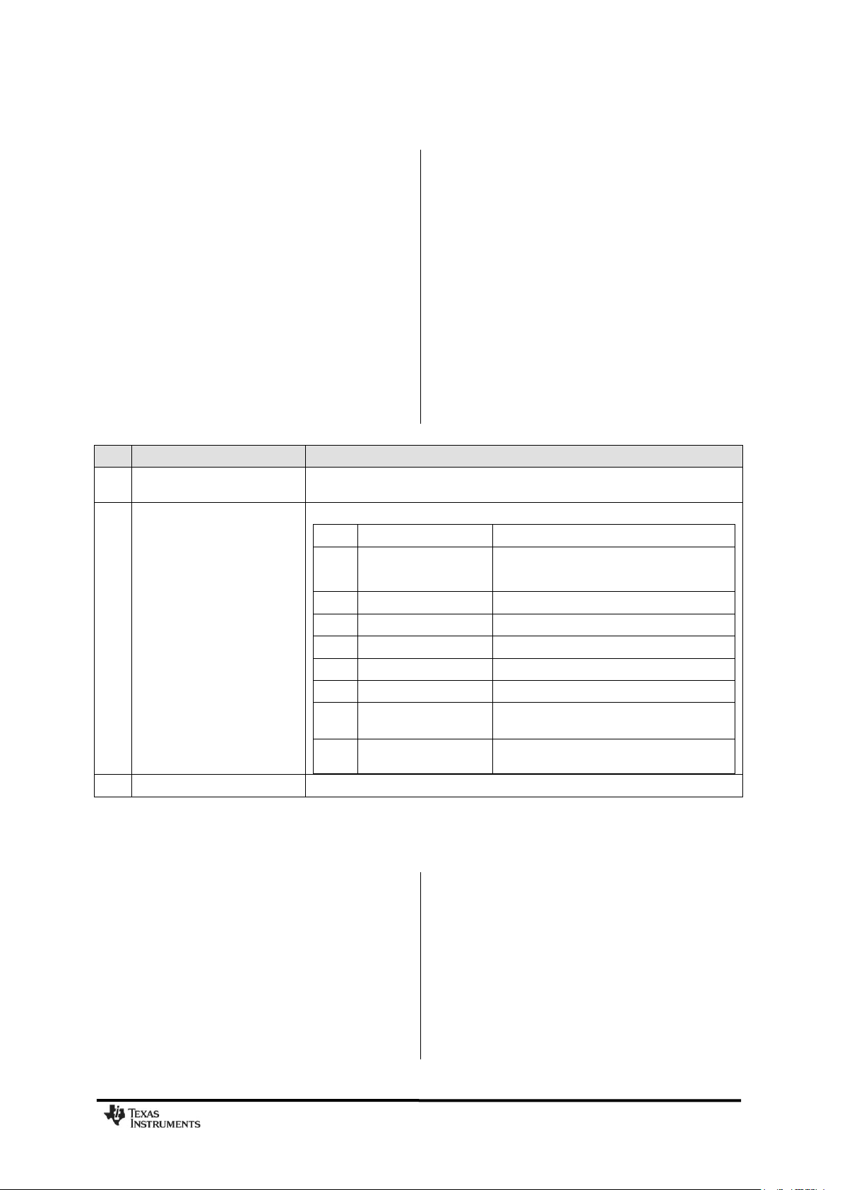
Bits
Name
Description
7
CHIP_RDYn
Stays high until power and crystal have stabilized. Should always be low when using
the SPI interface.
6:4
STATE[2:0]
Indicates the current main state machine mode
Value
State
Description
000
IDLE
IDLE state
(Also reported for some transitional states instead
of SETTLING or CALIBRATE)
001
RX
Receive mode
010
TX
Transmit mode
011
FSTXON
Fast TX ready
100
CALIBRATE
Frequency synthesizer calibration is running
101
SETTLING
PLL is settling
110
RXFIFO_OVERFLOW
RX FIFO has overflowed. Read out any
useful data, then flush the FIFO with SFRX
111
TXFIFO_UNDERFLOW
TX FIFO has underflowed. Acknowledge with
SFTX
3:0
FIFO_BYTES_AVAILABLE[3:0]
The number of bytes available in the RX FIFO or free bytes in the TX FIFO
10.1 Chip Status Byte
CC1101
When the header byte, data byte, or command
strobe is sent on the SPI interface, the chip
status byte is sent by the
CC1101
on the SO pin.
The status byte contains key status signals,
useful for the MCU. The first bit, s7, is the
CHIP_RDYn signal and this signal must go low
before the first positive edge of SCLK. The
CHIP_RDYn signal indicates that the crystal is
running.
Bits 6, 5, and 4 comprise the STATE value.
This value reflects the state of the chip. The
XOSC and power to the digital core are on in
the IDLE state, but all other modules are in
power down. The frequency and channel
configuration should only be updated when the
chip is in this state. The RX state will be active
when the chip is in receive mode. Likewise, TX
is active when the chip is transmitting.
The last four bits (3:0) in the status byte
contains FIFO_BYTES_AVAILABLE. For read
operations (the R/W¯ bit in the header byte is
set to 1), the FIFO_BYTES_AVAILABLE field
contains the number of bytes available for
reading from the RX FIFO. For write
operations (the R/W¯ bit in the header byte is
set to 0), the FIFO_BYTES_AVAILABLE field
contains the number of bytes that can be
written to the TX FIFO. When
FIFO_BYTES_AVAILABLE=15, 15 or more
bytes are available/free.
Table 23 gives a status byte summary.
Table 23: Status Byte Summary
10.2 Register Access
The configuration registers on the
CC1101
are
located on SPI addresses from 0x00 to 0x2E.
Table 43 on page 68 lists all configuration
registers. It is highly recommended to use
SmartRF Studio [5] to generate optimum
register settings. The detailed description of
each register is found in Section 29.1 and
29.2, starting on page 71. All configuration
registers can be both written to and read. The
R/W¯ bit controls if the register should be
written to or read. When writing to registers,
SWRS061H Page 31 of 98
the status byte is sent on the SO pin each time
a header byte or data byte is transmitted on
the SI pin. When reading from registers, the
status byte is sent on the SO pin each time a
header byte is transmitted on the SI pin.
Registers with consecutive addresses can be
accessed in an efficient way by setting the
burst bit (B) in the header byte. The address
bits (A5 – A0) set the start address in an
internal address counter. This counter is
incremented by one each new byte (every 8
Page 32
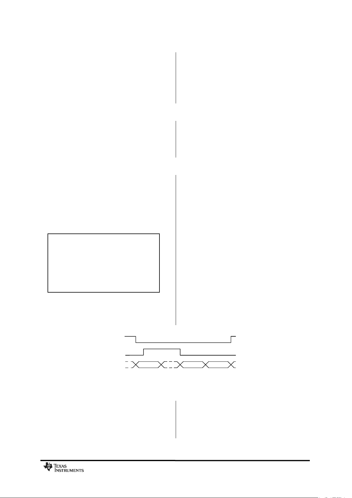
SI
Header
SRES
Header
Addr
Data
SO
CSn
Note: An SIDLE strobe will clear all
pending command strobes until IDLE
state is reached. This means that if for
example an SIDLE strobe is issued
while the radio is in RX state, any other
command strobes issued before the
radio reaches IDLE state will be
ignored.
CC1101
clock pulses). The burst access is either a
read or a write access and must be terminated
by setting CSn high.
For register addresses in the range 0x300x3D, the burst bit is used to select between
status registers when burst bit is one, and
between command strobes when burst bit is
10.3 SPI Read
When reading register fields over the SPI
interface while the register fields are updated
by the radio hardware (e.g. MARCSTATE or
TXBYTES), there is a small, but finite,
probability that a single read from the register
10.4 Command Strobes
Command Strobes may be viewed as single
byte instructions to
CC1101
. By addressing a
command strobe register, internal sequences
will be started. These commands are used to
disable the crystal oscillator, enable receive
mode, enable wake-on-radio etc. The 13
command strobes are listed in Table 42 on
page 67.
The command strobe registers are accessed
by transferring a single header byte (no data is
being transferred). That is, only the R/W¯ bit,
the burst access bit (set to 0), and the six
zero. See more in Section 10.3 below.
Because of this, burst access is not available
for status registers and they must be accessed
one at a time. The status registers can only be
read.
is being corrupt. As an example, the
probability of any single read from TXBYTES
being corrupt, assuming the maximum data
rate is used, is approximately 80 ppm. Refer to
the
CC1101
Errata Notes [3] for more details.
address bits (in the range 0x30 through 0x3D)
are written. The R/W¯ bit can be either one or
zero and will determine how the
FIFO_BYTES_AVAILABLE field in the status
byte should be interpreted.
When writing command strobes, the status
byte is sent on the SO pin.
A command strobe may be followed by any
other SPI access without pulling CSn high.
However, if an SRES strobe is being issued,
one will have to wait for SO to go low again
before the next header byte can be issued as
shown in Figure 16. The command strobes are
executed immediately, with the exception of
the SPWD, SWOR, and the SXOFF strobes,
which are executed when CSn goes high.
10.5 FIFO Access
The 64-byte TX FIFO and the 64-byte RX
FIFO are accessed through the 0x3F address.
When the R/W¯ bit is zero, the TX FIFO is
accessed, and the RX FIFO is accessed when
the R/W¯ bit is one.
SWRS061H Page 32 of 98
Figure 16: SRES Command Strobe
The TX FIFO is write-only, while the RX FIFO
is read-only.
The burst bit is used to determine if the FIFO
access is a single byte access or a burst
access. The single byte access method
Page 33

Read or write consecutive
Read or write n + 1 bytes
registers (burst):
from/to the RX/TX FIFO:
Header
Strobe
Header
Strobe
Header
Strobe
Header
Reg
Header
Reg n
Header
FIFO
Header
Reg
Data
Data
n
Data
Byte 0
Data
Header
Reg
Data Header
Reg
Data
Data
n + 1
Data
n + 2
Header
Strobe
Header
Reg
Data Header
Strobe
Header
FIFO
Data
Byte 1
Data
Byte 2
Data
Byte n - 1
Data
Byte n
Data
Byte 0
Data
Byte 1
CSn:
Command strobe(s):
Read or write register(s):
Combinations:
CC1101
expects a header byte with the burst bit set to
zero and one data byte. After the data byte, a
new header byte is expected; hence, CSn can
remain low. The burst access method expects
one header byte and then consecutive data
bytes until terminating the access by setting
CSn high.
The following header bytes access the FIFOs:
0x3F: Single byte access to TX FIFO
0x7F: Burst access to TX FIFO
0xBF: Single byte access to RX FIFO
0xFF: Burst access to RX FIFO
When writing to the TX FIFO, the status byte
(see Section 10.1) is output on SO for each
new data byte as shown in Figure 15. This
status byte can be used to detect TX FIFO
10.6 PATABLE Access
The 0x3E address is used to access the
PATABLE, which is used for selecting PA
power control settings. The SPI expects up to
eight data bytes after receiving the address.
By programming the PATABLE, controlled PA
power ramp-up and ramp-down can be
achieved, as well as ASK modulation shaping
for reduced bandwidth. See SmartRF Studio
[5] for recommended shaping / PA ramping
sequences. See also Section 24 for details on
output power programming.
The PATABLE is an 8-byte table that defines
the PA control settings to use for each of the
eight PA power values (selected by the 3-bit
value FREND0.PA_POWER). The table is
written and read from the lowest setting (0) to
the highest (7), one byte at a time. An index
counter is used to control the access to the
table. This counter is incremented each time a
byte is read or written to the table, and set to
the lowest index when CSn is high. When the
underflow while writing data to the TX FIFO.
Note that the status byte contains the number
of bytes free before writing the byte in
progress to the TX FIFO. When the last byte
that fits in the TX FIFO is transmitted on SI,
the status byte received concurrently on SO
will indicate that one byte is free in the TX
FIFO.
The TX FIFO may be flushed by issuing a
SFTX command strobe. Similarly, a SFRX
command strobe will flush the RX FIFO. A
SFTX or SFRX command strobe can only be
issued in the IDLE, TXFIFO_UNDERFLOW, or
RXFIFO_OVERFLOW states. Both FIFOs are
flushed when going to the SLEEP state.
Figure 17 gives a brief overview of different
register access types possible.
highest value is reached the counter restarts
at zero.
The access to the PATABLE is either single
byte or burst access depending on the burst
bit. When using burst access the index counter
will count up; when reaching 7 the counter will
restart at 0. The R/W¯ bit controls whether the
access is a read or a write access.
If one byte is written to the PATABLE and this
value is to be read out, CSn must be set high
before the read access in order to set the
index counter back to zero.
Note that the content of the PATABLE is lost
when entering the SLEEP state, except for the
first byte (index 0).
For more information, see Design Note DN501
[18].
Figure 17: Register Access Types
SWRS061H Page 33 of 98
Page 34
CSn
SCLK
SI
Function
1 X X
Chip unaffected by SCLK/SI
0 0 Generates SPWD strobe
0 1 Generates STX strobe
1 0 Generates SIDLE strobe
1
1
Generates SRX strobe
0
SPI
mode
SPI
mode
SPI mode (wakes up into
IDLE if in SLEEP/XOFF)
11 Microcontroller Interface and Pin Configuration
CC1101
In a typical system,
CC1101
will interface to a
microcontroller. This microcontroller must be
able to:
Program
CC1101
into different modes
11.1 Configuration Interface
The microcontroller uses four I/O pins for the
SPI configuration interface (SI, SO, SCLK and
11.2 General Control and Status Pins
The
CC1101
has two dedicated configurable
pins (GDO0 and GDO2) and one shared pin
(GDO1) that can output internal status
information useful for control software. These
pins can be used to generate interrupts on the
MCU. See Section 26 on page 61 for more
details on the signals that can be
programmed.
GDO1 is shared with the SO pin in the SPI
interface. The default setting for GDO1/SO is
3-state output. By selecting any other of the
programming options, the GDO1/SO pin will
become a generic pin. When CSn is low, the
pin will always function as a normal SO pin.
In the synchronous and asynchronous serial
modes, the GDO0 pin is used as a serial TX
data input pin while in transmit mode.
Read and write buffered data
Read back status information via the 4-wire
SPI-bus configuration interface (SI, SO,
SCLK and CSn)
CSn). The SPI is described in Section 10 on
page 29.
The GDO0 pin can also be used for an on-chip
analog temperature sensor. By measuring the
voltage on the GDO0 pin with an external
ADC, the temperature can be calculated.
Specifications for the temperature sensor are
found in Section 4.7. With default PTEST
register setting (0x7F), the temperature sensor
output is only available if the frequency
synthesizer is enabled (e.g. the MANCAL,
FSTXON, RX, and TX states). It is necessary
to write 0xBF to the PTEST register to use the
analog temperature sensor in the IDLE state.
Before leaving the IDLE state, the PTEST
register should be restored to its default value
(0x7F).
11.3 Optional Radio Control Feature
The
CC1101
has an optional way of controlling
the radio by reusing SI, SCLK, and CSn from
the SPI interface. This feature allows for a
simple three-pin control of the major states of
the radio: SLEEP, IDLE, RX, and TX. This
optional functionality is enabled with the
MCSM0.PIN_CTRL_EN configuration bit.
State changes are commanded as follows:
If CSn is high, the SI and SCLK are set to
the desired state according to Table 24.
If CSn goes low, the state of SI and SCLK
is latched and a command strobe is
generated internally according to the pin
configuration.
It is only possible to change state with the
latter functionality. That means that for
instance RX will not be restarted if SI and
SCLK are set to RX and CSn toggles. When
CSn is low the SI and SCLK has normal SPI
functionality.
All pin control command strobes are executed
immediately except the SPWD strobe. The
SPWD strobe is delayed until CSn goes high.
Table 24: Optional Pin Control Coding
SWRS061H Page 34 of 98
Page 35

XOSC
EDRATE
DATA
f
MDRATE
R
28
_
2
2_256
256
2
2
_
2
log_
_
28
20
2
EDRATE
XOSC
DATA
XOSC
DATA
f
R
MDRATE
f
R
EDRATE
Min Data
Rate
[kBaud]
Typical Data
Rate
[kBaud]
Max Data
Rate
[kBaud]
Data rate
Step Size
[kBaud]
0.6
1.0
0.79
0.0015
0.79
1.2
1.58
0.0031
1.59
2.4
3.17
0.0062
3.17
4.8
6.33
0.0124
6.35
9.6
12.7
0.0248
12.7
19.6
25.3
0.0496
25.4
38.4
50.7
0.0992
50.8
76.8
101.4
0.1984
101.6
153.6
202.8
0.3967
203.1
250
405.5
0.7935
406.3
500
500
1.5869
ECHANBW
XOSC
channel
MCHANBW
f
BW
_
2)·_4(8
MDMCFG4.
CHANBW_M
MDMCFG4.CHANBW_E
00
01
10
11
00
812
406
203
102
01
650
325
162
81
10
541
270
135
68
11
464
232
116
58
12 Data Rate Programming
CC1101
The data rate used when transmitting, or the
data rate expected in receive is programmed
by the MDMCFG3.DRATE_M and the
MDMCFG4.DRATE_E configuration registers.
The data rate is given by the formula below.
As the formula shows, the programmed data
rate depends on the crystal frequency.
The following approach can be used to find
suitable values for a given data rate:
If DRATE_M is rounded to the nearest integer
and becomes 256, increment DRATE_E and
use DRATE_M = 0.
The data rate can be set from 0.6 kBaud to
500 kBaud with the minimum step size
according to Table 25 below. See Table 3 for
the minimum and maximum data rates for the
different modulation formats.
Table 25: Data Rate Step Size (assuming a
26 MHz crystal)
13 Receiver Channel Filter Bandwidth
In order to meet different channel width
requirements, the receiver channel filter is
programmable. The MDMCFG4.CHANBW_E and
MDMCFG4.CHANBW_M configuration registers
control the receiver channel filter bandwidth,
which scales with the crystal oscillator
frequency.
The following formula gives the relation
between the register settings and the channel
filter bandwidth:
Table 26 lists the channel filter bandwidths
supported by the
CC1101
.
Table 26: Channel Filter Bandwidths [kHz]
(assuming a 26 MHz crystal)
By compensating for a frequency offset
between the transmitter and the receiver, the
filter bandwidth can be reduced and the
sensitivity improved, see more in DN005 [17]
and in Section 14.1.
SWRS061H Page 35 of 98
Page 36
Note: Frequency offset compensation is
not supported for ASK or OOK modulation.
14 Demodulator, Symbol Synchronizer, and Data Decision
CC1101
CC1101
contains an advanced and highly
configurable demodulator. Channel filtering
and frequency offset compensation is
performed digitally. To generate the RSSI level
14.1 Frequency Offset Compensation
The
CC1101
has a very fine frequency
resolution (see Table 15). This feature can be
used to compensate for frequency offset and
drift.
When using 2-FSK, GFSK, 4-FSK, or MSK
modulation, the demodulator will compensate
for the offset between the transmitter and
receiver frequency within certain limits, by
estimating the centre of the received data. The
frequency offset compensation configuration is
controlled from the FOCCFG register. By
compensating for a large frequency offset
between the transmitter and the receiver, the
sensitivity can be improved, see DN005 [17].
The tracking range of the algorithm is
selectable as fractions of the channel
bandwidth with the FOCCFG.FOC_LIMIT
configuration register.
If the FOCCFG.FOC_BS_CS_GATE bit is set,
the offset compensator will freeze until carrier
sense asserts. This may be useful when the
radio is in RX for long periods with no traffic,
(see Section 17.3 for more information), the
signal level in the channel is estimated. Data
filtering is also included for enhanced
performance.
since the algorithm may drift to the boundaries
when trying to track noise.
The tracking loop has two gain factors, which
affects the settling time and noise sensitivity of
the algorithm. FOCCFG.FOC_PRE_K sets the
gain before the sync word is detected, and
FOCCFG.FOC_POST_K selects the gain after
the sync word has been found.
The estimated frequency offset value is
available in the FREQEST status register. This
can be used for permanent frequency offset
compensation. By writing the value from
FREQEST into FSCTRL0.FREQOFF, the
frequency synthesizer will automatically be
adjusted according to the estimated frequency
offset. More details regarding this permanent
frequency compensation algorithm can be
found in DN015 [10].
14.2 Bit Synchronization
The bit synchronization algorithm extracts the
clock from the incoming symbols. The
algorithm requires that the expected data rate
14.3 Byte Synchronization
Byte synchronization is achieved by a
continuous sync word search. The sync word
is a 16 bit configurable field (can be repeated
to get a 32 bit) that is automatically inserted at
the start of the packet by the modulator in
transmit mode. The MSB in the sync word is
sent first. The demodulator uses this field to
find the byte boundaries in the stream of bits.
The sync word will also function as a system
identifier, since only packets with the correct
predefined sync word will be received if the
sync word detection in RX is enabled in
register MDMCFG2 (see Section 17.1). The
sync word detector correlates against the
user-configured 16 or 32 bit sync word. The
is programmed as described in Section 12.
Re-synchronization is performed continuously
to adjust for error in the incoming symbol rate.
correlation threshold can be set to 15/16,
16/16, or 30/32 bits match. The sync word can
be further qualified using the preamble quality
indicator mechanism described below and/or a
carrier sense condition. The sync word is
configured through the SYNC1 and SYNC0
registers.
In order to make false detections of sync
words less likely, a mechanism called
preamble quality indication (PQI) can be used
to qualify the sync word. A threshold value for
the preamble quality must be exceeded in
order for a detected sync word to be accepted.
See Section 17.2 for more details.
SWRS061H Page 36 of 98
Page 37
Bit
Field Name
Description
7:0
RSSI
RSSI value
Bit
Field Name
Description
7
CRC_OK
1: CRC for received data OK
(or CRC disabled)
0: CRC error in received data
6:0
LQI
Indicating the link quality
Note: Register fields that control the
packet handling features should only be
altered when
CC1101
is in the IDLE state.
15 Packet Handling Hardware Support
The
CC1101
packet oriented radio protocols.
In transmit mode, the packet handler can be
configured to add the following elements to the
packet stored in the TX FIFO:
A programmable number of preamble
bytes
A two byte synchronization (sync) word.
Can be duplicated to give a 4-byte sync
word (recommended). It is not possible to
only insert preamble or only insert a sync
word
A CRC checksum computed over the data
field.
The recommended setting is 4-byte preamble
and 4-byte sync word, except for 500 kBaud
data rate where the recommended preamble
length is 8 bytes. In addition, the following can
be implemented on the data field and the
optional 2-byte CRC checksum:
Whitening of the data with a PN9
sequence
Forward Error Correction (FEC) by the use
of interleaving and coding of the data
(convolutional coding)
has built-in hardware support for
Preamble detection
Sync word detection
CRC computation and CRC check
One byte address check
Packet length check (length byte checked
against a programmable maximum length)
De-whitening
De-interleaving and decoding
Optionally, two status bytes (see Table 27 and
Table 28) with RSSI value, Link Quality
Indication, and CRC status can be appended
in the RX FIFO.
Table 27: Received Packet Status Byte 1
(first byte appended after the data)
Table 28: Received Packet Status Byte 2
(second byte appended after the data)
CC1101
In receive mode, the packet handling support
will de-construct the data packet by
implementing the following (if enabled):
15.1 Data Whitening
From a radio perspective, the ideal over the air
data are random and DC free. This results in
the smoothest power distribution over the
occupied bandwidth. This also gives the
regulation loops in the receiver uniform
operation conditions (no data dependencies).
Real data often contain long sequences of
zeros and ones. In these cases, performance
can be improved by whitening the data before
transmitting, and de-whitening the data in the
receiver.
With
CC1101
, this can be done automatically.
By setting PKTCTRL0.WHITE_DATA=1, all
data, except the preamble and the sync word
will be XOR-ed with a 9-bit pseudo-random
(PN9) sequence before being transmitted. This
is shown in Figure 18. At the receiver end, the
data are XOR-ed with the same pseudorandom sequence. In this way, the whitening is
reversed, and the original data appear in the
receiver. The PN9 sequence is initialized to all
1‟s.
SWRS061H Page 37 of 98
Page 38

TX_OUT[7:0]
TX_DATA
8 7 6 5 4 3 2 1 0
7 6 5 4 3 2 1 0
The first TX_DATA byte is shifted in before doing the XOR-operation providing the first TX_OUT[7:0] byte. The
second TX_DATA byte is then shifted in before doing the XOR-operation providing the second TX_OUT[7:0] byte.
Preamble bits
(1010...1010)
Sync word
Length field
Address field
Data field
CRC-16
Optional CRC-16 calculation
Optionally FEC encoded/decoded
8 x n bits 16/32 bits
8
bits8bits
8 x n bits 16 bits
Optional data whitening
Legend:
Inserted automatically in TX,
processed and removed in RX.
Optional user-provided fields processed in TX,
processed but not removed in RX.
Unprocessed user data (apart from FEC
and/or whitening)
Figure 18: Data Whitening in TX Mode
CC1101
15.2 Packet Format
The format of the data packet can be
configured and consists of the following items
(see Figure 19):
Preamble
Synchronization word
Figure 19: Packet Format
The preamble pattern is an alternating
sequence of ones and zeros (10101010…).
The minimum length of the preamble is
programmable through the value of
MDMCFG1.NUM_PREAMBLE. When enabling
TX, the modulator will start transmitting the
preamble. When the programmed number of
preamble bytes has been transmitted, the
modulator will send the sync word and then
data from the TX FIFO if data is available. If
the TX FIFO is empty, the modulator will
continue to send preamble bytes until the first
byte is written to the TX FIFO. The modulator
will then send the sync word and then the data
bytes.
SWRS061H Page 38 of 98
Optional length byte
Optional address byte
Payload
Optional 2 byte CRC
The synchronization word is a two-byte value
set in the SYNC1 and SYNC0 registers. The
sync word provides byte synchronization of the
incoming packet. A one-byte sync word can be
emulated by setting the SYNC1 value to the
preamble pattern. It is also possible to emulate
a 32 bit sync word by setting
MDMCFG2.SYNC_MODE to 3 or 7. The sync
word will then be repeated twice.
CC1101
supports both constant packet length
protocols and variable length protocols.
Variable or fixed packet length mode can be
used for packets up to 255 bytes. For longer
Page 39
Note: The minimum packet length
supported (excluding the optional length
byte and CRC) is one byte of payload
data.
CC1101
packets, infinite packet length mode must be
used.
Fixed packet length mode is selected by
setting PKTCTRL0.LENGTH_CONFIG=0. The
desired packet length is set by the PKTLEN
register. This value must be different from 0.
In variable packet length mode,
PKTCTRL0.LENGTH_CONFIG=1, the packet
length is configured by the first byte after the
sync word. The packet length is defined as the
payload data, excluding the length byte and
the optional CRC. The PKTLEN register is
used to set the maximum packet length
allowed in RX. Any packet received with a
length byte with a value greater than PKTLEN
will be discarded. The PKTLEN value must be
different from 0.The first byte written to the
TXFIFO must be different from 0.
With PKTCTRL0.LENGTH_CONFIG=2, the
packet length is set to infinite and transmission
and reception will continue until turned off
manually. As described in the next section,
this can be used to support packet formats
with different length configuration than natively
supported by
that TX mode is not turned off during the
transmission of the first half of any byte. Refer
to the
CC1101
CC1101
. One should make sure
Errata Notes [3] for more details.
the packet. Then the PKTLEN value is set
according to this value. The end of packet will
occur when the byte counter in the packet
handler is equal to the PKTLEN register. Thus,
the MCU must be able to program the correct
length, before the internal counter reaches the
packet length.
15.2.2 Packet Length > 255
The packet automation control register,
PKTCTRL0, can be reprogrammed during TX
and RX. This opens the possibility to transmit
and receive packets that are longer than 256
bytes and still be able to use the packet
handling hardware support. At the start of the
packet, the infinite packet length mode
(PKTCTRL0.LENGTH_CONFIG=2) must be
active. On the TX side, the PKTLEN register is
set to mod(length, 256). On the RX side the
MCU reads out enough bytes to interpret the
length field in the packet and sets the PKTLEN
register to mod(length, 256). When less than
256 bytes remains of the packet, the MCU
disables infinite packet length mode and
activates fixed packet length mode. When the
internal byte counter reaches the PKTLEN
value, the transmission or reception ends (the
radio enters the state determined by
TXOFF_MODE or RXOFF_MODE). Automatic
CRC appending/checking can also be used
(by setting PKTCTRL0.CRC_EN=1).
15.2.1 Arbitrary Length Field Configuration
The packet length register, PKTLEN, can be
reprogrammed during receive and transmit. In
combination with fixed packet length mode
(PKTCTRL0.LENGTH_CONFIG=0), this opens
the possibility to have a different length field
configuration than supported for variable
length packets (in variable packet length mode
the length byte is the first byte after the sync
word). At the start of reception, the packet
length is set to a large value. The MCU reads
out enough bytes to interpret the length field in
When for example a 600-byte packet is to be
transmitted, the MCU should do the following
(see also Figure 20)
Set PKTCTRL0.LENGTH_CONFIG=2.
Pre-program the PKTLEN register to
mod(600, 256) = 88.
Transmit at least 345 bytes (600 - 255), for
example by filling the 64-byte TX FIFO six
times (384 bytes transmitted).
Set PKTCTRL0.LENGTH_CONFIG=0.
The transmission ends when the packet
counter reaches 88. A total of 600 bytes
are transmitted.
SWRS061H Page 39 of 98
Page 40
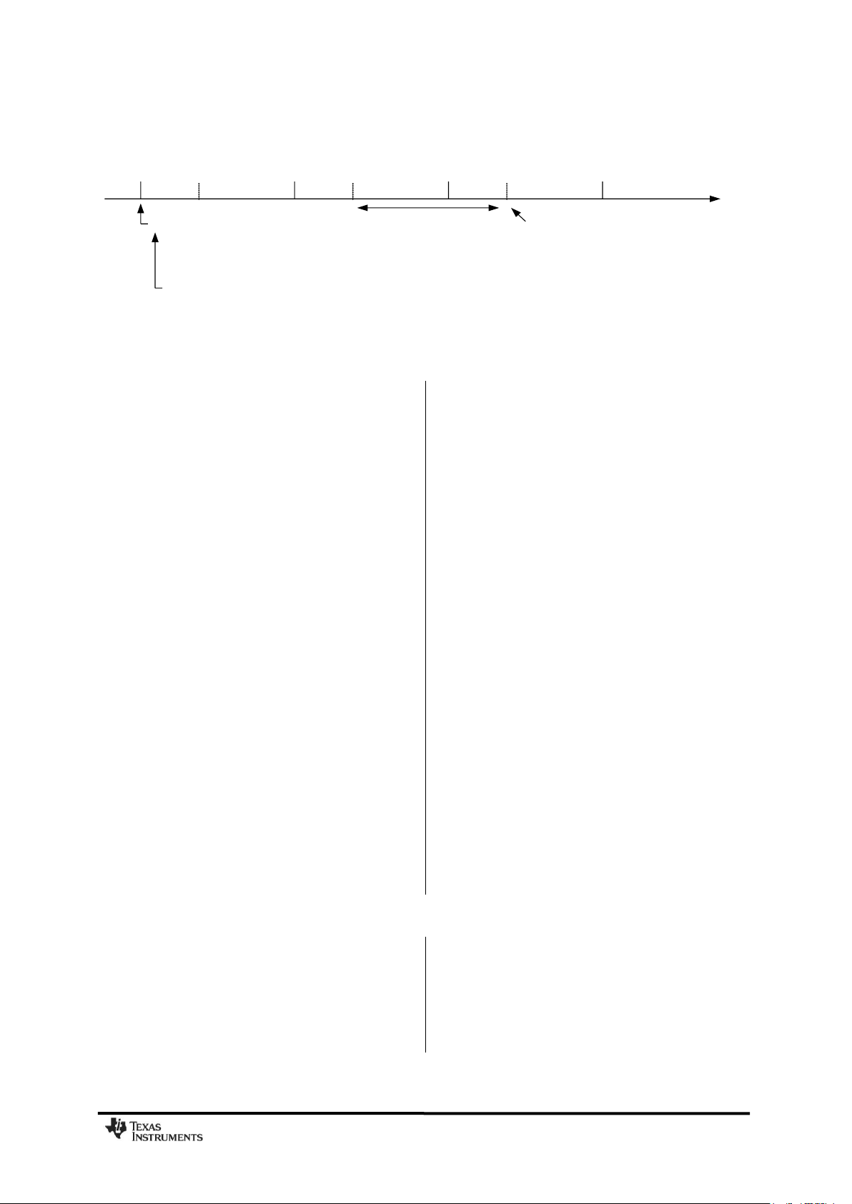
0,1,..........,88,....................255,0,........,88,..................,255,0,........,88,..................,255,0,.......................
Internal byte counter in packet handler counts from 0 to 255 and then starts at 0 again
Length field transmitted and received. Rx and Tx PKTLEN value set to mod(600,256) = 88
Infinite packet length enabled
Fixed packet length
enabled when less than
256 bytes remains of
packet
600 bytes transmitted and
received
Figure 20: Packet Length > 255
15.3 Packet Filtering in Receive Mode
CC1101
CC1101
packet-filtering; address filtering, maximum
length filtering, and CRC filtering.
15.3.1 Address Filtering
Setting PKTCTRL1.ADR_CHK to any other
value than zero enables the packet address
filter. The packet handler engine will compare
the destination address byte in the packet with
the programmed node address in the ADDR
register and the 0x00 broadcast address when
PKTCTRL1.ADR_CHK=10 or both the 0x00
and 0xFF broadcast addresses when
PKTCTRL1.ADR_CHK=11. If the received
address matches a valid address, the packet
is received and written into the RX FIFO. If the
address match fails, the packet is discarded
and receive mode restarted (regardless of the
MCSM1.RXOFF_MODE setting).
If the received address matches a valid
address when using infinite packet length
mode and address filtering is enabled, 0xFF
will be written into the RX FIFO followed by the
address byte and then the payload data.
15.3.2 Maximum Length Filtering
In variable packet length mode,
PKTCTRL0.LENGTH_CONFIG=1, the
PKTLEN.PACKET_LENGTH register value is
supports three different types of
used to set the maximum allowed packet
length. If the received length byte has a larger
value than this, the packet is discarded and
receive mode restarted (regardless of the
MCSM1.RXOFF_MODE setting).
15.3.3 CRC Filtering
The filtering of a packet when CRC check fails
is enabled by setting
PKTCTRL1.CRC_AUTOFLUSH=1. The CRC
auto flush function will flush the entire RX
FIFO if the CRC check fails. After auto flushing
the RX FIFO, the next state depends on the
MCSM1.RXOFF_MODE setting.
When using the auto flush function, the
maximum packet length is 63 bytes in variable
packet length mode and 64 bytes in fixed
packet length mode. Note that when
PKTCTRL1.APPEND_STATUS is enabled, the
maximum allowed packet length is reduced by
two bytes in order to make room in the RX
FIFO for the two status bytes appended at the
end of the packet. Since the entire RX FIFO is
flushed when the CRC check fails, the
previously received packet must be read out of
the FIFO before receiving the current packet.
The MCU must not read from the current
packet until the CRC has been checked as
OK.
15.4 Packet Handling in Transmit Mode
The payload that is to be transmitted must be
written into the TX FIFO. The first byte written
must be the length byte when variable packet
length is enabled. The length byte has a value
equal to the payload of the packet (including
the optional address byte). If address
recognition is enabled on the receiver, the
SWRS061H Page 40 of 98
second byte written to the TX FIFO must be
the address byte.
If fixed packet length is enabled, the first byte
written to the TX FIFO should be the address
(assuming the receiver uses address
recognition).
Page 41

CC1101
The modulator will first send the programmed
number of preamble bytes. If data is available
in the TX FIFO, the modulator will send the
two-byte (optionally 4-byte) sync word followed
by the payload in the TX FIFO. If CRC is
enabled, the checksum is calculated over all
the data pulled from the TX FIFO, and the
result is sent as two extra bytes following the
payload data. If the TX FIFO runs empty
before the complete packet has been
transmitted, the radio will enter
TXFIFO_UNDERFLOW state. The only way to
exit this state is by issuing an SFTX strobe.
15.5 Packet Handling in Receive Mode
In receive mode, the demodulator and packet
handler will search for a valid preamble and
the sync word. When found, the demodulator
has obtained both bit and byte synchronization
and will receive the first payload byte.
If FEC/Interleaving is enabled, the FEC
decoder will start to decode the first payload
byte. The interleaver will de-scramble the bits
before any other processing is done to the
data.
If whitening is enabled, the data will be dewhitened at this stage.
When variable packet length mode is enabled,
the first byte is the length byte. The packet
handler stores this value as the packet length
and receives the number of bytes indicated by
Writing to the TX FIFO after it has underflowed
will not restart TX mode.
If whitening is enabled, everything following
the sync words will be whitened. This is done
before the optional FEC/Interleaver stage.
Whitening is enabled by setting
PKTCTRL0.WHITE_DATA=1.
If FEC/Interleaving is enabled, everything
following the sync words will be scrambled by
the interleaver and FEC encoded before being
modulated. FEC is enabled by setting
MDMCFG1.FEC_EN=1.
the length byte. If fixed packet length mode is
used, the packet handler will accept the
programmed number of bytes.
Next, the packet handler optionally checks the
address and only continues the reception if the
address matches. If automatic CRC check is
enabled, the packet handler computes CRC
and matches it with the appended CRC
checksum.
At the end of the payload, the packet handler
will optionally write two extra packet status
bytes (see Table 27 and Table 28) that contain
CRC status, link quality indication, and RSSI
value.
15.6 Packet Handling in Firmware
When implementing a packet oriented radio
protocol in firmware, the MCU needs to know
when a packet has been received/transmitted.
Additionally, for packets longer than 64 bytes,
the RX FIFO needs to be read while in RX and
the TX FIFO needs to be refilled while in TX.
This means that the MCU needs to know the
number of bytes that can be read from or
written to the RX FIFO and TX FIFO
respectively. There are two possible solutions
to get the necessary status information:
a) Interrupt Driven Solution
The GDO pins can be used in both RX and TX
to give an interrupt when a sync word has
been received/transmitted or when a complete
packet has been received/transmitted by
setting IOCFGx.GDOx_CFG=0x06. In addition,
there are two configurations for the
IOCFGx.GDOx_CFG register that can be used
as an interrupt source to provide information
on how many bytes that are in the RX FIFO
and TX FIFO respectively. The
IOCFGx.GDOx_CFG=0x00 and the
IOCFGx.GDOx_CFG=0x01 configurations are
associated with the RX FIFO while the
IOCFGx.GDOx_CFG=0x02 and the
IOCFGx.GDOx_CFG=0x03 configurations
are associated with the TX FIFO. See Table
41 for more information.
b) SPI Polling
The PKTSTATUS register can be polled at a
given rate to get information about the current
GDO2 and GDO0 values respectively. The
RXBYTES and TXBYTES registers can be
polled at a given rate to get information about
the number of bytes in the RX FIFO and TX
FIFO respectively. Alternatively, the number of
bytes in the RX FIFO and TX FIFO can be
read from the chip status byte returned on the
SWRS061H Page 41 of 98
Page 42
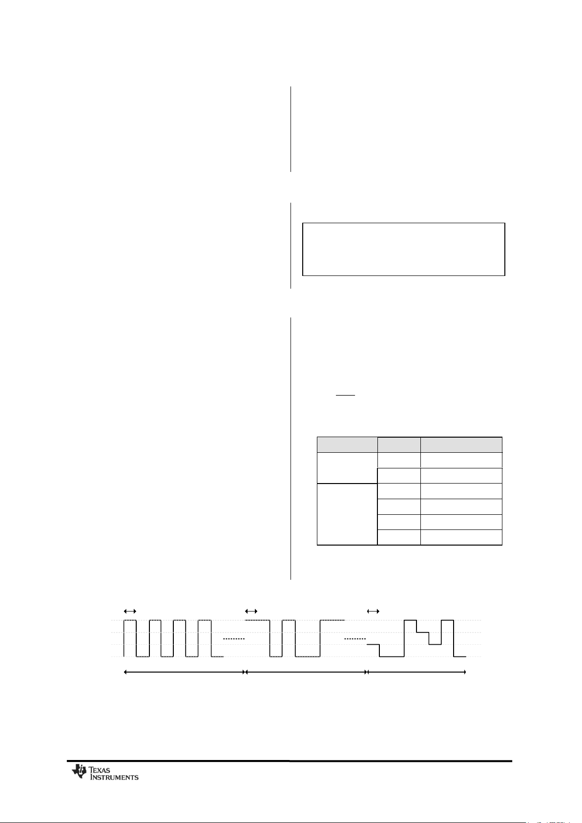
EDEVIATION
xosc
dev
MDEVIATION
f
f
_
17
2)_8(
2
Format
Symbol
Coding
2-FSK/GFSK
„0‟
– Deviation
„1‟
+ Deviation
4-FSK
„01‟
– Deviation
„00‟
– 1/3∙ Deviation
„10‟
+1/3∙ Deviation
„11‟
+ Deviation
+1
+1/3
-1/3
-1
1 0 1 0 1 0 1 0 1 1 0 1 0 0 1 1 00 01 01 11 10 00 11 01
Preamble
0xAA
Sync
0xD3
Data
0x17 0x8D
1/Baud Rate 1/Baud Rate 1/Baud Rate
Note: Manchester encoding is not
supported at the same time as using the
FEC/Interleaver option or when using MSK
and 4-FSK modulation.
CC1101
MISO line each time a header byte, data byte,
or command strobe is sent on the SPI bus.
It is recommended to employ an interrupt
driven solution since high rate SPI polling
reduces the RX sensitivity. Furthermore, as
explained in Section 10.3 and the
CC1101
Errata Notes [3], when using SPI polling, there
16 Modulation Formats
CC1101
supports amplitude, frequency, and
phase shift modulation formats. The desired
modulation format is set in the
MDMCFG2.MOD_FORMAT register.
Optionally, the data stream can be Manchester
coded by the modulator and decoded by the
demodulator. This option is enabled by setting
16.1 Frequency Shift Keying
CC1101
supports both 2-FSK and 4-FSK
modulation. 2-FSK can optionally be shaped
by a Gaussian filter with BT = 0.5, producing a
GFSK modulated signal. This spectrumshaping feature improves adjacent channel
power (ACP) and occupied bandwidth. When
selecting 4-FSK, the preamble and sync word
is sent using 2-FSK (see Figure 21).
In „true‟ 2-FSK systems with abrupt frequency
shifting, the spectrum is inherently broad. By
making the frequency shift „softer‟, the
spectrum can be made significantly narrower.
Thus, higher data rates can be transmitted in
the same bandwidth using GFSK.
is a small, but finite, probability that a single
read from registers PKTSTATUS , RXBYTES
and TXBYTES is being corrupt. The same is
the case when reading the chip status byte.
Refer to the TI website for SW examples ([6]
and [7]).
MDMCFG2.MANCHESTER_EN=1.
The frequency deviation is programmed with
the DEVIATION_M and DEVIATION_E values
in the DEVIATN register. The value has an
exponent/mantissa form, and the resultant
deviation is given by:
The symbol encoding is shown in Table 29.
When 2-FSK/GFSK/4-FSK modulation is used,
the DEVIATN register specifies the expected
frequency deviation of incoming signals in RX
and should be the same as the TX deviation
for demodulation to be performed reliably and
robustly.
Figure 21: Data Sent Over the Air (MDMCFG2.MOD_FORMAT=100)
SWRS061H Page 42 of 98
Table 29: Symbol Encoding for 2-FSK/GFSK
and 4-FSK Modulation
Page 43

2
16.2 Minimum Shift Keying
CC1101
When using MSK2, the complete transmission
(preamble, sync word, and payload) will be
MSK modulated.
Phase shifts are performed with a constant
transition time. The fraction of a symbol period
used to change the phase can be modified
with the DEVIATN.DEVIATION_M setting.
Identical to offset QPSK with half-sine
shaping (data coding may differ).
16.3 Amplitude Modulation
CC1101
supports two different forms of
amplitude modulation: On-Off Keying (OOK)
and Amplitude Shift Keying (ASK).
OOK modulation simply turns the PA on or off
to modulate ones and zeros respectively.
The ASK variant supported by the
allows programming of the modulation depth
(the difference between 1 and 0), and shaping
of the pulse amplitude. Pulse shaping
CC1101
This is equivalent to changing the shaping of
the symbol. The DEVIATN register setting has
no effect in RX when using MSK.
When using MSK, Manchester
encoding/decoding should be disabled by
setting MDMCFG2.MANCHESTER_EN=0.
The MSK modulation format implemented in
CC1101
inverts the sync word and data
compared to e.g. signal generators.
produces a more bandwidth constrained
output spectrum.
When using OOK/ASK, the AGC settings from
the SmartRF Studio [5] preferred FSK/MSK
settings are not optimum. DN022 [16] give
guidelines on how to find optimum OOK/ASK
settings from the preferred settings in
SmartRF Studio [5]. The DEVIATN register
setting has no effect in either TX or RX when
using OOK/ASK.
17 Received Signal Qualifiers and Link Quality Information
CC1101
has several qualifiers that can be used
to increase the likelihood that a valid sync
word is detected:
Sync Word Qualifier
Preamble Quality Threshold
17.1 Sync Word Qualifier
If sync word detection in RX is enabled in the
MDMCFG2 register, the
filling the RX FIFO and perform the packet
filtering described in Section 15.3 before a
valid sync word has been detected. The sync
CC1101
will not start
RSSI
Carrier Sense
Clear Channel Assessment
Link Quality Indicator
word qualifier mode is set by
MDMCFG2.SYNC_MODE and is summarized in
Table 30. Carrier sense in Table 30 is
described in Section 17.4.
SWRS061H Page 43 of 98
Page 44

MDMCFG2.SYNC_MODE
Sync Word Qualifier Mode
000
No preamble/sync
001
15/16 sync word bits detected
010
16/16 sync word bits detected
011
30/32 sync word bits detected
100
No preamble/sync + carrier sense
above threshold
101
15/16 + carrier sense above threshold
110
16/16 + carrier sense above threshold
111
30/32 + carrier sense above threshold
LENGTHFILTER
channel
RSSI
BW
f
_
282
Note: It takes some time from the radio
enters RX mode until a valid RSSI value is
present in the RSSI register. Please see
DN505 [12] for details on how the RSSI
response time can be estimated.
Table 30: Sync Word Qualifier Mode
17.2 Preamble Quality Threshold (PQT)
CC1101
The Preamble Quality Threshold (PQT) sync
word qualifier adds the requirement that the
received sync word must be preceded with a
preamble with a quality above the
programmed threshold.
Another use of the preamble quality threshold
is as a qualifier for the optional RX termination
timer. See Section 19.7 for details.
The preamble quality estimator increases an
internal counter by one each time a bit is
received that is different from the previous bit,
and decreases the counter by eight each time
a bit is received that is the same as the last bit.
17.3 RSSI
The RSSI value is an estimate of the signal
power level in the chosen channel. This value
is based on the current gain setting in the RX
chain and the measured signal level in the
channel.
In RX mode, the RSSI value can be read
continuously from the RSSI status register
until the demodulator detects a sync word
(when sync word detection is enabled). At that
point the RSSI readout value is frozen until the
next time the chip enters the RX state.
The threshold is configured with the register
field PKTCTRL1.PQT. A threshold of 4∙PQT for
this counter is used to gate sync word
detection. By setting the value to zero, the
preamble quality qualifier of the sync word is
disabled.
A “Preamble Quality Reached” signal can be
observed on one of the GDO pins by setting
IOCFGx.GDOx_CFG=8. It is also possible to
determine if preamble quality is reached by
checking the PQT_REACHED bit in the
PKTSTATUS register. This signal / bit asserts
when the received signal exceeds the PQT.
(BW
is defined in Section 13) and
channel
AGCCTRL0.FILTER_LENGTH.
If PKTCTRL1.APPEND_STATUS is enabled,
the last RSSI value of the packet is
automatically added to the first byte appended
after the payload.
The RSSI value read from the RSSI status
register is a 2‟s complement number. The
following procedure can be used to convert the
RSSI reading to an absolute power level
(RSSI_dBm)
The RSSI value is given in dBm with a ½ dB
resolution. The RSSI update rate, f
depends on the receiver filter bandwidth
SWRS061H Page 44 of 98
RSSI
1) Read the RSSI status register
2) Convert the reading from a hexadecimal
number to a decimal number (RSSI_dec)
3) If RSSI_dec ≥ 128 then RSSI_dBm =
,
(RSSI_dec - 256)/2 – RSSI_offset
Page 45

Data rate [kBaud]
RSSI_offset [dB], 433 MHz
RSSI_offset [dB], 868 MHz
1.2
74
74
38.4
74
74
250
74
74
500
74
74
-120
-110
-100
-90
-80
-70
-60
-50
-40
-30
-20
-10 0 -120
-110
-100
-90
-80
-70
-60
-50
-40
-30
-20
-10
0
Input Power [dBm]
RSSI Readout [dBm]
1.2 kBaud
38.4 kBaud
250 kBaud
500 kBaud
CC1101
4) Else if RSSI_dec < 128 then RSSI_dBm =
(RSSI_dec)/2 – RSSI_offset
Table 31 gives typical values for the
RSSI_offset. Figure 22 and Figure 23 show
Table 31: Typical RSSI_offset Values
typical plots of RSSI readings as a function of
input power level for different data rates.
Figure 22: Typical RSSI Value vs. Input Power Level for Different Data Rates at 433 MHz
SWRS061H Page 45 of 98
Page 46
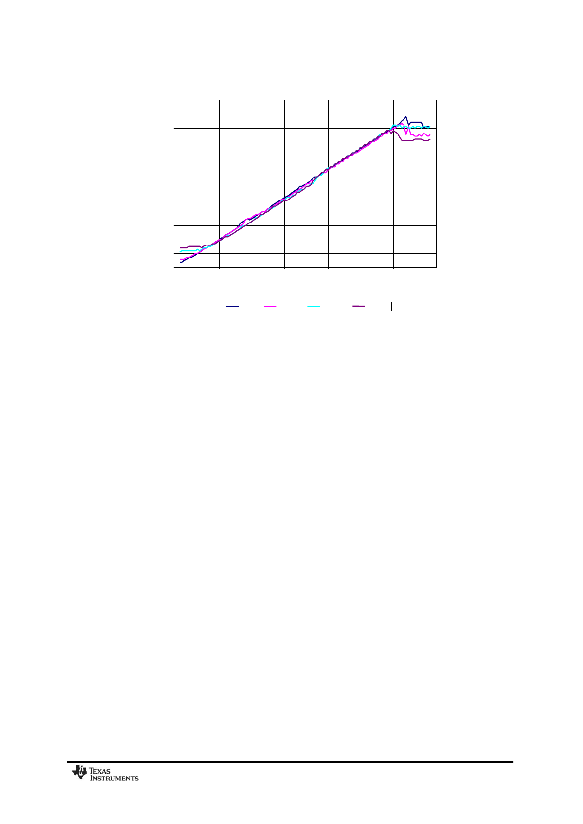
-120
-110
-100
-90
-80
-70
-60
-50
-40
-30
-20
-10 0 -120
-110
-100
-90
-80
-70
-60
-50
-40
-30
-20
-10
0
Input Power [dBm]
RSSI Readout [dBm]
1.2 kBaud
38.4 kBaud
250 kBaud
500 kBaud
CC1101
Figure 23: Typical RSSI Value vs. Input Power Level for Different Data Rates at 868 MHz
17.4 Carrier Sense (CS)
Carrier sense (CS) is used as a sync word
qualifier and for Clear Channel Assessment
(see Section 17.5). CS can be asserted based
on two conditions which can be individually
adjusted:
CS is asserted when the RSSI is above a
programmable absolute threshold, and deasserted when RSSI is below the same
threshold (with hysteresis). See more in
Section 17.4.1.
CS is asserted when the RSSI has
optional fast RX termination (see Section
19.7).
CS can be used to avoid interference from
other RF sources in the ISM bands.
17.4.1 CS Absolute Threshold
The absolute threshold related to the RSSI
value depends on the following register fields:
AGCCTRL2.MAX_LNA_GAIN
AGCCTRL2.MAX_DVGA_GAIN
increased with a programmable number of
dB from one RSSI sample to the next, and
de-asserted when RSSI has decreased
with the same number of dB. This setting
is not dependent on the absolute signal
level and is thus useful to detect signals in
environments with time varying noise floor.
See more in Section 17.4.2.
Carrier sense can be used as a sync word
qualifier that requires the signal level to be
higher than the threshold for a sync word
search to be performed and is set by setting
MDMCFG2 The carrier sense signal can be
observed on one of the GDO pins by setting
IOCFGx.GDOx_CFG=14 and in the status
register bit PKTSTATUS.CS.
Other uses of Carrier sense include the TX-ifCCA function (see Section 17.5) and the
SWRS061H Page 46 of 98
AGCCTRL1.CARRIER_SENSE_ABS_THR
AGCCTRL2.MAGN_TARGET
For given AGCCTRL2.MAX_LNA_GAIN and
AGCCTRL2.MAX_DVGA_GAIN settings, the
absolute threshold can be adjusted ±7 dB in
steps of 1 dB using
CARRIER_SENSE_ABS_THR.
The MAGN_TARGET setting is a compromise
between blocker tolerance/selectivity and
sensitivity. The value sets the desired signal
level in the channel into the demodulator.
Increasing this value reduces the headroom
for blockers, and therefore close-in selectivity.
It is strongly recommended to use SmartRF
Studio [5] to generate the correct
MAGN_TARGET setting. Table 32 and Table
Page 47
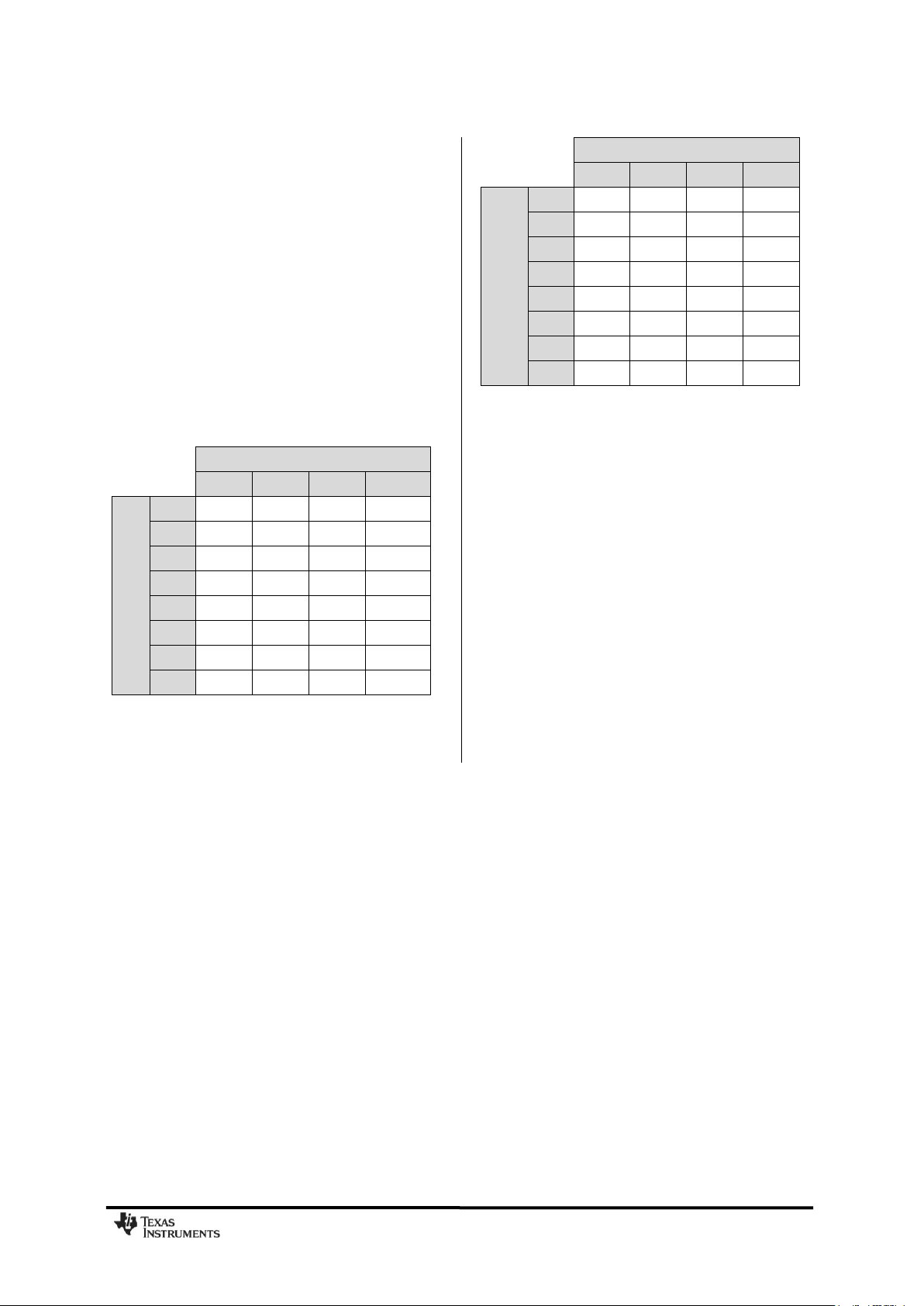
MAX_DVGA_GAIN[1:0]
00
01
10
11
MAX_LNA_GAIN[2:0]
000
-97.5
-91.5
-85.5
-79.5
001
-94
-88
-82.5
-76
010
-90.5
-84.5
-78.5
-72.5
011
-88
-82.5
-76.5
-70.5
100
-85.5
-80
-73.5
-68
101
-84
-78
-72
-66
110
-82
-76
-70
-64
111
-79
-73.5
-67
-61
MAX_DVGA_GAIN[1:0]
00
01
10
11
MAX_LNA_GAIN[2:0]
000
-90.5
-84.5
-78.5
-72.5
001
-88
-82
-76
-70
010
-84.5
-78.5
-72
-66
011
-82.5
-76.5
-70
-64
100
-80.5
-74.5
-68
-62
101
-78
-72
-66
-60
110
-76.5
-70
-64
-58
111
-74.5
-68
-62
-56
33 show the typical RSSI readout values at the
CS threshold at 2.4 kBaud and 250 kBaud
data rate respectively. The default reset value
for CARRIER_SENSE_ABS_THR = 0 (0 dB) has
been used. MAGN_TARGET = 3 (33 dB) and 7
(42 dB) have been used for 2.4 kBaud and
250 kBaud data rate respectively. For other
data rates, the user must generate similar
tables to find the CS absolute threshold.
If the threshold is set high, i.e. only strong
signals are wanted, the threshold should be
adjusted upwards by first reducing the
MAX_LNA_GAIN value and then the
MAX_DVGA_GAIN value. This will reduce
power consumption in the receiver front end,
since the highest gain settings are avoided.
Table 33: Typical RSSI Value in dBm at CS
Threshold with MAGN_TARGET = 7 (42 dB) at
250 kBaud, 868 MHz
17.4.2 CS Relative Threshold
The relative threshold detects sudden changes
in the measured signal level. This setting does
not depend on the absolute signal level and is
thus useful to detect signals in environments
with a time varying noise floor. The register
field AGCCTRL1.CARRIER_SENSE_REL_THR
is used to enable/disable relative CS, and to
select threshold of 6 dB, 10 dB, or 14 dB RSSI
change.
CC1101
Table 32: Typical RSSI Value in dBm at CS
Threshold with MAGN_TARGET = 3 (33 dB) at
2.4 kBaud, 868 MHz
SWRS061H Page 47 of 98
Page 48
lengthpacket
BERPER
_
)1(1
17.5 Clear Channel Assessment (CCA)
CC1101
The Clear Channel Assessment (CCA) is used
to indicate if the current channel is free or
busy. The current CCA state is viewable on
any of the GDO pins by setting
IOCFGx.GDOx_CFG=0x09.
MCSM1.CCA_MODE selects the mode to use
when determining CCA.
When the STX or SFSTXON command strobe is
given while
FSTXON state is only entered if the clear
channel requirements are fulfilled. Otherwise,
the chip will remain in RX. If the channel then
17.6 Link Quality Indicator (LQI)
The Link Quality Indicator is a metric of the
current quality of the received signal. If
PKTCTRL1.APPEND_STATUS is enabled, the
value is automatically added to the last byte
appended after the payload. The value can
also be read from the LQI status register. The
LQI gives an estimate of how easily a received
signal can be demodulated by accumulating
CC1101
is in the RX state, the TX or
becomes available, the radio will not enter TX
or FSTXON state before a new strobe
command is sent on the SPI interface. This
feature is called TX-if-CCA. Four CCA
requirements can be programmed:
Always (CCA disabled, always goes to TX)
If RSSI is below threshold
Unless currently receiving a packet
Both the above (RSSI below threshold and
not currently receiving a packet)
the magnitude of the error between ideal
constellations and the received signal over the
64 symbols immediately following the sync
word. LQI is best used as a relative
measurement of the link quality (a low value
indicates a better link than what a high value
does), since the value is dependent on the
modulation format.
18 Forward Error Correction with Interleaving
18.1 Forward Error Correction (FEC)
CC1101
has built in support for Forward Error
Correction (FEC). To enable this option, set
MDMCFG1.FEC_EN to 1. FEC is only supported
in fixed packet length mode, i.e. when
PKTCTRL0.LENGTH_CONFIG=0. FEC is
employed on the data field and CRC word in
order to reduce the gross bit error rate when
operating near the sensitivity limit.
Redundancy is added to the transmitted data
in such a way that the receiver can restore the
original data in the presence of some bit
errors.
The use of FEC allows correct reception at a
lower Signal-to-Noise Ratio (SNR), thus
extending communication range if the receiver
bandwidth remains constant. Alternatively, for
a given SNR, using FEC decreases the bit
error rate (BER). The packet error rate (PER)
is related to BER by
A lower BER can therefore be used to allow
longer packets, or a higher percentage of
packets of a given length, to be transmitted
successfully. Finally, in realistic ISM radio
environments, transient and time-varying
phenomena will produce occasional errors
even in otherwise good reception conditions.
FEC will mask such errors and, combined with
interleaving of the coded data, even correct
relatively long periods of faulty reception (burst
errors).
The FEC scheme adopted for
convolutional coding, in which n bits are
generated based on k input bits and the m
most recent input bits, forming a code stream
able to withstand a certain number of bit errors
between each coding state (the m-bit window).
The convolutional coder is a rate ½ code with
a constraint length of m = 4. The coder codes
one input bit and produces two output bits;
hence, the effective data rate is halved. This
means that in order to transmit at the same
effective data rate when using FEC, it is
necessary to use twice as high over-the-air
data rate. This will require a higher receiver
bandwidth, and thus reduce sensitivity. In
other words the improved reception by using
FEC and the degraded sensitivity from a
higher receiver bandwidth will be
counteracting factors. See Design Note
DN504 for more details [19].
CC1101
is
SWRS061H Page 48 of 98
Page 49
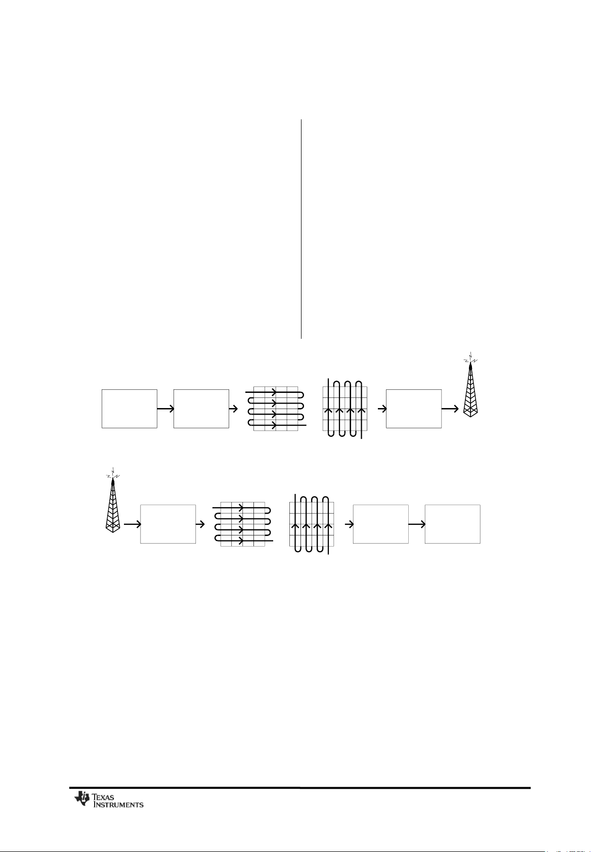
Packet
Engine
FEC
Encoder
Modulator
Interleaver
Write buffer
Interleaver
Read buffer
Demodulator
FEC
Decoder
Packet
Engine
Interleaver
Write buffer
Interleaver
Read buffer
18.2 Interleaving
CC1101
Data received through radio channels will
often experience burst errors due to
interference and time-varying signal strengths.
In order to increase the robustness to errors
spanning multiple bits, interleaving is used
when FEC is enabled. After de-interleaving, a
continuous span of errors in the received
stream will become single errors spread apart.
CC1101
employs matrix interleaving, which is
illustrated in Figure 24. The on-chip
interleaving and de-interleaving buffers are 4 x
4 matrices. In the transmitter, the data bits
from the rate ½ convolutional coder are written
into the rows of the matrix, whereas the bit
sequence to be transmitted is read from the
columns of the matrix. Conversely, in the
receiver, the received symbols are written into
the rows of the matrix, whereas the data
passed onto the convolutional decoder is read
from the columns of the matrix.
CC1101
employs a 4x4 matrix interleaver with 2
bits (one encoder output symbol) per cell and
the amount of data transmitted over the air will
thus always be a multiple of four bytes (see
DN507 [20] for more details). When FEC and
interleaving is used, at least one extra byte is
required for trellis termination and the packet
control hardware therefore automatically
inserts one or two extra bytes at the end of the
packet. These bytes will be invisible to the
user, as they are removed before the received
packet enters the RXFIFO.
When FEC and interleaving is used the
minimum data payload is 2 bytes.
Figure 24: General Principle of Matrix Interleaving
SWRS061H Page 49 of 98
Page 50
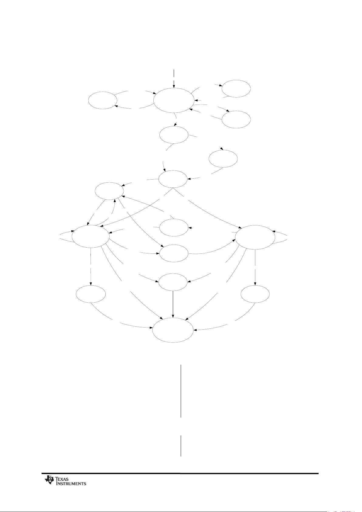
TX
19,20
RX
13,14,15
IDLE
1
CALIBRATE
8
MANCAL
3,4,5
SETTLING
9,10,11
RX_OVERFLOW
17
TX_UNDERFLOW
22
RXTX_SETTLING
21
FSTXON
18
SFSTXON
FS_AUTOCAL = 00 | 10 | 11
&
SRX | STX | SFSTXON | WOR
SRX | WOR
STX
STX
TXFIFO_UNDERFLOW
STX | RXOFF_MODE = 10
RXOFF_MODE = 00
&
FS_AUTOCAL = 10 | 11
SFTX
SRX | TXOFF_MODE = 11
SIDLE
SCAL
CAL_COMPLETE
FS_AUTOCAL = 01
&
SRX | STX | SFSTXON | WOR
RXFIFO_OVERFLOW
CAL_COMPLETE
SFRX
CALIBRATE
12
IDLE
1
TXOFF_MODE = 00
&
FS_AUTOCAL = 10 | 11
RXOFF_MODE = 00
&
FS_AUTOCAL = 00 | 01
TXOFF_MODE = 00
&
FS_AUTOCAL = 00 | 01
TXOFF_MODE = 10
RXOFF_MODE = 11
SFSTXON | RXOFF_MODE = 01
TXRX_SETTLING
16
SRX | STX | SFSTXON | WOR
SLEEP
0
SPWD | SWOR
XOFF
2
SXOFF
CSn = 0
CSn = 0 | WOR
( STX | SFSTXON ) & CCA
|
RXOFF_MODE = 01 | 10
TXOFF_MODE=01
FS_WAKEUP
6,7
SRX
19 Radio Control
CC1101
CC1101
has a built-in state machine that is used
to switch between different operational states
(modes). The change of state is done either by
Figure 25: Complete Radio Control State Diagram
using command strobes or by internal events
such as TX FIFO underflow.
A simplified state diagram, together with
typical usage and current consumption, is
19.1 Power-On Start-Up Sequence
When the power supply is turned on, the
system must be reset. This is achieved by one
of the two sequences described below, i.e.
shown in Figure 13 on page 28. The complete
radio control state diagram is shown in Figure
25. The numbers refer to the state number
readable in the MARCSTATE status register.
This register is primarily for test purposes.
automatic power-on reset (POR) or manual
reset. After the automatic power-on reset or
manual reset, it is also recommended to
SWRS061H Page 50 of 98
Page 51
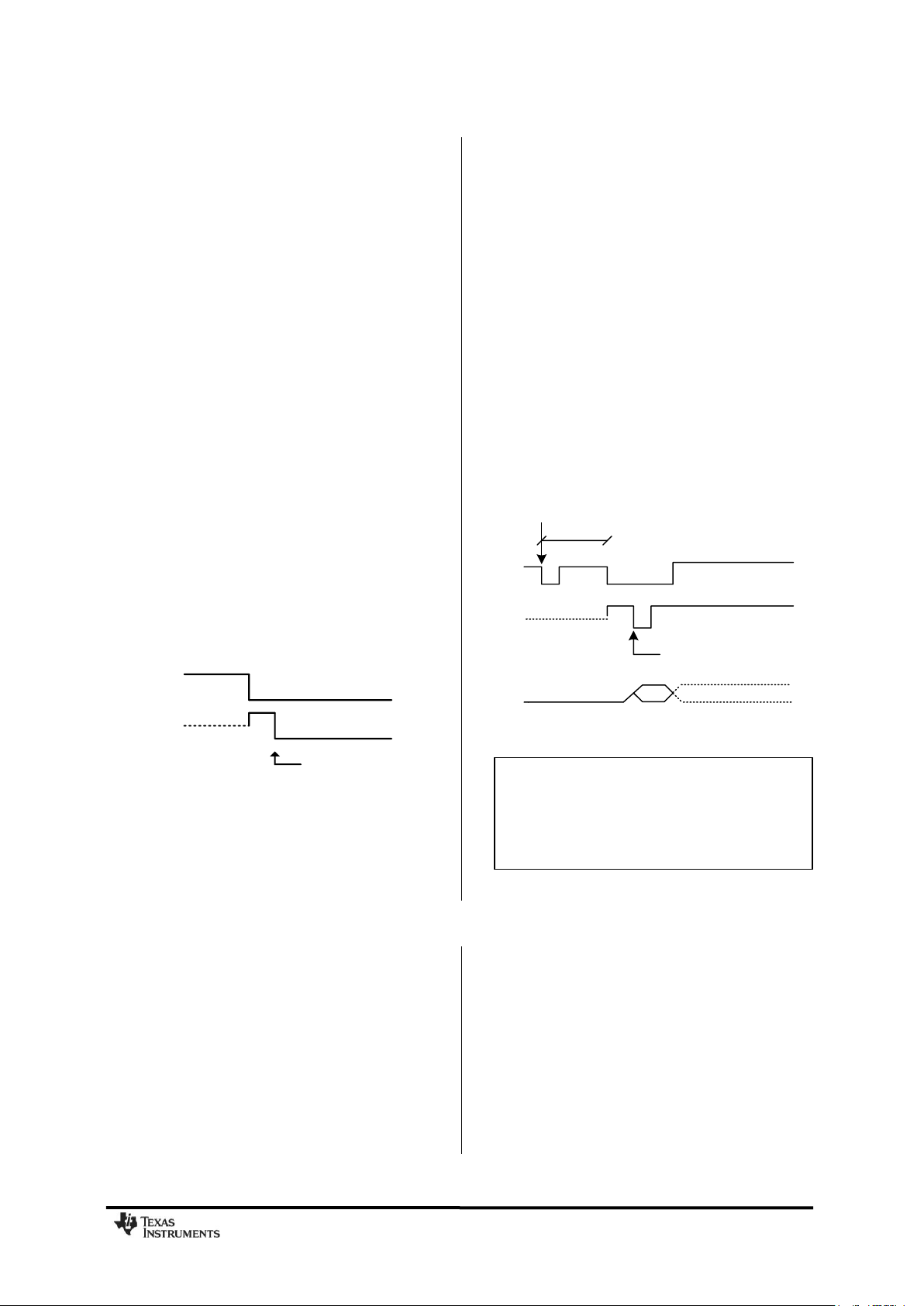
XOSC Stable
CSn
SO
CSn
SO
XOSC Stable
XOSC and voltage regulator switched on
SI
SRES
40 us
Note that the above reset procedure is
only required just after the power supply is
first turned on. If the user wants to reset
the
CC1101
after this, it is only necessary to
issue an SRES command strobe.
CC1101
change the signal that is output on the GDO0
pin. The default setting is to output a clock
signal with a frequency of CLK_XOSC/192.
However, to optimize performance in TX and
RX, an alternative GDO setting from the
settings found in Table 41 on page 62 should
be selected.
19.1.1 Automatic POR
A power-on reset circuit is included in the
CC1101
. The minimum requirements stated in
Table 18 must be followed for the power-on
reset to function properly. The internal powerup sequence is completed when CHIP_RDYn
goes low. CHIP_RDYn is observed on the SO
pin after CSn is pulled low. See Section 10.1
for more details on CHIP_RDYn.
When the
will be in the IDLE state and the crystal
oscillator will be running. If the chip has had
sufficient time for the crystal oscillator to
stabilize after the power-on-reset, the SO pin
will go low immediately after taking CSn low. If
CSn is taken low before reset is completed,
the SO pin will first go high, indicating that the
crystal oscillator is not stabilized, before going
low as shown in Figure 26.
CC1101
reset is completed, the chip
this strobe, all internal registers and states are
set to the default, IDLE state. The manual
power-up sequence is as follows (see Figure
27):
Set SCLK = 1 and SI = 0, to avoid
potential problems with pin control mode
(see Section 11.3).
Strobe CSn low / high.
Hold CSn low and then high for at least 40
µs relative to pulling CSn low
Pull CSn low and wait for SO to go low
(CHIP_RDYn).
Issue the SRES strobe on the SI line.
When SO goes low again, reset is
complete and the chip is in the IDLE state.
Figure 26: Power-On Reset
19.1.2 Manual Reset
The other global reset possibility on
uses the SRES command strobe. By issuing
19.2 Crystal Control
The crystal oscillator (XOSC) is either
automatically controlled or always on, if
MCSM0.XOSC_FORCE_ON is set.
In the automatic mode, the XOSC will be
turned off if the SXOFF or SPWD command
strobes are issued; the state machine then
goes to XOFF or SLEEP respectively. This
can only be done from the IDLE state. The
XOSC will be turned off when CSn is released
(goes high). The XOSC will be automatically
turned on again when CSn goes low. The
SWRS061H Page 51 of 98
CC1101
Figure 27: Power-On Reset with SRES
state machine will then go to the IDLE state.
The SO pin on the SPI interface must be
pulled low before the SPI interface is ready to
be used as described in Section 10.1.
If the XOSC is forced on, the crystal will
always stay on even in the SLEEP state.
Crystal oscillator start-up time depends on
crystal ESR and load capacitances. The
electrical specification for the crystal oscillator
can be found in Section 4.4.
Page 52
3
Note: When MCSM1.RXOFF_MODE=11
and a packet has been received, it will
take some time before a valid RSSI value
is present in the RSSI register again even
if the radio has never exited RX mode.
This time is the same as the RSSI
response time discussed in DN505 [12].
19.3 Voltage Regulator Control
CC1101
The voltage regulator to the digital core is
controlled by the radio controller. When the
chip enters the SLEEP state which is the state
with the lowest current consumption, the
voltage regulator is disabled. This occurs after
CSn is released when a SPWD command
strobe has been sent on the SPI interface. The
19.4 Active Modes (RX and TX)
CC1101
has two active modes: receive and
transmit. These modes are activated directly
by the MCU by using the SRX and STX
command strobes, or automatically by Wake
on Radio.
The frequency synthesizer must be calibrated
regularly.
option (using the SCAL strobe), and three
automatic calibration options that are
controlled by the MCSM0.FS_AUTOCAL setting:
Calibrate when going from IDLE to either
Calibrate when going from either RX or TX
CC1101
has one manual calibration
RX or TX (or FSTXON)
to IDLE automatically3
chip is then in the SLEEP state. Setting CSn
low again will turn on the regulator and crystal
oscillator and make the chip enter the IDLE
state.
When Wake on Radio is enabled, the WOR
module will control the voltage regulator as
described in Section19.5.
IDLE
FSTXON: Frequency synthesizer on and
ready at the TX frequency. Activate TX
with STX
TX: Start sending preamble
RX: Start search for a new packet
Calibrate every fourth time when going
from either RX or TX to IDLE
automatically3
If the radio goes from TX or RX to IDLE by
issuing an SIDLE strobe, calibration will not be
performed. The calibration takes a constant
number of XOSC cycles; see Table 34 for
timing details regarding calibration.
When RX is activated, the chip will remain in
receive mode until a packet is successfully
received or the RX termination timer expires
(see Section 19.7). The probability that a false
sync word is detected can be reduced by
using PQT, CS, maximum sync word length,
and sync word qualifier mode as described in
Section 17. After a packet is successfully
received, the radio controller goes to the state
indicated by the MCSM1.RXOFF_MODE setting.
The possible destinations are:
Not forced in IDLE by issuing an SIDLE
strobe
Similarly, when TX is active the chip will
remain in the TX state until the current packet
has been successfully transmitted. Then the
state will change as indicated by the
MCSM1.TXOFF_MODE setting. The possible
destinations are the same as for RX.
The MCU can manually change the state from
RX to TX and vice versa by using the
command strobes. If the radio controller is
currently in transmit and the SRX strobe is
used, the current transmission will be ended
and the transition to RX will be done.
If the radio controller is in RX when the STX or
SFSTXON command strobes are used, the TXif-CCA function will be used. If the channel is
not clear, the chip will remain in RX. The
MCSM1.CCA_MODE setting controls the
conditions for clear channel assessment. See
Section 17.5 for details.
The SIDLE command strobe can always be
used to force the radio controller to go to the
IDLE state.
SWRS061H Page 52 of 98
Page 53
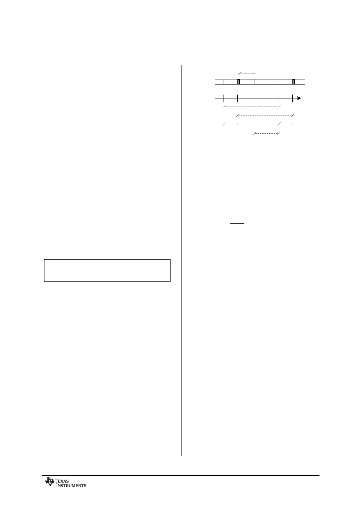
RESWOR
XOSC
Event
EVENT
f
t
_5
0
20
750
t
Event0
t
Event1
Event1Event0 Event1 Event0
t
Event1
t
Event0
t
State: IDLESLEEP RX SLEEP IDLE
RX
Rx timeout
t
SLEEP
128
750
XOSC
f
Note: The FIFO looses its content in the
SLEEP state.
19.5 Wake On Radio (WOR)
The optional Wake on Radio (WOR)
functionality enables
wake up from SLEEP and listen for incoming
packets without MCU interaction.
When the SWOR strobe command is sent on
the SPI interface, the
SLEEP state when CSn is released. The RC
oscillator must be enabled before the SWOR
strobe can be used, as it is the clock source
for the WOR timer. The on-chip timer will set
CC1101
into IDLE state and then RX state. After
a programmable time in RX, the chip will go
back to the SLEEP state, unless a packet is
received. See Figure 28 and Section 19.7 for
details on how the timeout works.
To exit WOR mode, set the
IDLE state
CC1101
can be set up to signal the MCU that a
packet has been received by using the GDO
pins. If a packet is received, the
MCSM1.RXOFF_MODE will determine the
behaviour at the end of the received packet.
When the MCU has read the packet, it can put
the chip back into SLEEP with the SWOR strobe
from the IDLE state.
CC1101
to periodically
CC1101
will go to the
CC1101
into the
Figure 28: Event 0 and Event 1 Relationship
The time from the
CC1101
enters SLEEP state
until the next Event0 is programmed to
appear, t
in Figure 28, should be larger
SLEEP
than 11.08 ms when using a 26 MHz crystal
and 10.67 ms when a 27 MHz crystal is used.
If t
is less than 11.08 (10.67) ms, there is
SLEEP
a chance that the consecutive Event 0 will
occur
seconds
too early. Application Note AN047 [4] explains
in detail the theory of operation and the
different registers involved when using WOR,
as well as highlighting important aspects when
using WOR mode.
CC1101
The WOR timer has two events, Event 0 and
Event 1. In the SLEEP state with WOR
activated, reaching Event 0 will turn on the
digital regulator and start the crystal oscillator.
Event 1 follows Event 0 after a programmed
timeout.
The time between two consecutive Event 0 is
programmed with a mantissa value given by
WOREVT1.EVENT0 and WOREVT0.EVENT0,
and an exponent value set by
WORCTRL.WOR_RES. The equation is:
The Event 1 timeout is programmed with
WORCTRL.EVENT1. Figure 28 shows the
timing relationship between Event 0 timeout
and Event 1 timeout.
SWRS061H Page 53 of 98
19.5.1 RC Oscillator and Timing
The frequency of the low-power RC oscillator
used for the WOR functionality varies with
temperature and supply voltage. In order to
keep the frequency as accurate as possible,
the RC oscillator will be calibrated whenever
possible, which is when the XOSC is running
and the chip is not in the SLEEP state. When
the power and XOSC are enabled, the clock
used by the WOR timer is a divided XOSC
clock. When the chip goes to the sleep state,
the RC oscillator will use the last valid
calibration result. The frequency of the RC
oscillator is locked to the main crystal
frequency divided by 750.
In applications where the radio wakes up very
often, typically several times every second, it
is possible to do the RC oscillator calibration
once and then turn off calibration to reduce the
current consumption. This is done by setting
WORCTRL.RC_CAL=0 and requires that RC
oscillator calibration values are read from
registers RCCTRL0_STATUS and
RCCTRL1_STATUS and written back to
Page 54

Description
Transition Time
(no PA ramping)
Transition Time [µs]
IDLE to RX, no calibration
1953/f
xosc
75.1
IDLE to RX, with calibration
1953/f
xosc
+ FS calibration Time
799
IDLE to TX/FSTXON, no calibration
1954/f
xosc
75.2
IDLE to TX/FSTXON, with calibration
1953/f
xosc
+ FS calibration Time
799
TX to RX switch
782/f
xosc
+ 0.25/f
baudrate
31.1
RX to TX switch
782/f
xosc
30.1
TX to IDLE, no calibration
~0.25/f
baudrate
~1
TX to IDLE, with calibration
~0.25/f
baudrate
+ FS calibration Time
725
RX to IDLE, no calibration
2/f
xosc
~0.1
RX to IDLE, with calibration
2/f
xosc
+ FS calibration Time
724
Manual calibration
283/f
xosc
+ FS calibration Time
735
CC1101
RCCTRL0 and RCCTRL1 respectively. If the
RC oscillator calibration is turned off, it will
have to be manually turned on again if
19.6 Timing
19.6.1 Overall State Transition Times
The main radio controller needs to wait in
certain states in order to make sure that the
internal analog/digital parts have settled down
and are ready to operate in the new states. A
number of factors are important for the state
transition times:
The crystal oscillator frequency, f
xosc
PA ramping enabled or not
The data rate in cases where PA ramping
is enabled
The value of the TEST0, TEST1, and
FSCAL3 registers
temperature and supply voltage changes.
Refer to Application Note AN047 [4] for further
details.
Table 34 shows timing in crystal clock cycles
for key state transitions.
Power on time and XOSC start-up times are
variable, but within the limits stated in Table
13.
Note that TX to IDLE and TX to RX transition
times are functions of data rate (f
baudrate
). When
PA ramping is enabled (i.e.
FREND0.PA_POWER≠000
), TX to IDLE and
b
TX to RX will require
(FREND0.PA_POWER)/8∙f
baudrate
longer times
than the times stated in Table 34.
Table 34: Overall State Transition Times (Example for 26 MHz crystal oscillator, 250 kBaud data
19.6.2 Frequency Synthesizer Calibration
Time
Table 35 summarizes the frequency
synthesizer (FS) calibration times for possible
settings of TEST0 and
FSCAL3.CHP_CURR_CAL_EN. Setting
FSCAL3.CHP_CURR_CAL_EN to 00b disables
the charge pump calibration stage. TEST0 is
set to the values recommended by SmartRF
Studio software [5]. The possible values for
rate, and TEST0 = 0x0B (maximum calibration time)).
TEST0 when operating with different frequency
bands are 0x09 and 0x0B. SmartRF Studio
software [5] always sets
FSCAL3.CHP_CURR_CAL_EN to 10b.
Note that in a frequency hopping spread
spectrum or a multi-channel protocol the
calibration time can be reduced from 712/724
µs to 145/157 µs. This is explained in Section
28.2.
SWRS061H Page 54 of 98
Page 55
TEST0
FSCAL3.CHP_CURR_CAL_EN
FS Calibration Time
f
xosc
= 26 MHz
FS Calibration Time
f
xosc
= 27 MHz
0x09
00b
3764/f
xosc =
145 us
3764/f
xosc =
139 us
0x09
10b
18506/f
xosc =
712 us
18506/f
xosc =
685 us
0x0B
00b
4073/f
xosc =
157 us
4073/f
xosc =
151 us
0x0B
10b
18815/f
xosc =
724 us
18815/f
xosc =
697 us
Table 35: Frequency Synthesizer Calibration Times (26/27 MHz crystal)
19.7 RX Termination Timer
CC1101
CC1101
has optional functions for automatic
termination of RX after a programmable time.
The main use for this functionality is Wake on
Radio, but it may also be useful for other
applications. The termination timer starts when
in RX state. The timeout is programmable with
the MCSM2.RX_TIME setting. When the timer
expires, the radio controller will check the
condition for staying in RX; if the condition is
not met, RX will terminate.
The programmable conditions are:
MCSM2.RX_TIME_QUAL=0: Continue
receive if sync word has been found
MCSM2.RX_TIME_QUAL=1: Continue
receive if sync word has been found, or if
the preamble quality is above threshold
(PQT)
If the system expects the transmission to have
started when enabling the receiver, the
MCSM2.RX_TIME_RSSI function can be used.
The radio controller will then terminate RX if
the first valid carrier sense sample indicates
no carrier (RSSI below threshold). See Section
17.4 for details on Carrier Sense.
For ASK/OOK modulation, lack of carrier
sense is only considered valid after eight
symbol periods. Thus, the
MCSM2.RX_TIME_RSSI function can be used
in ASK/OOK mode when the distance between
“1” symbols is eight or less.
If RX terminates due to no carrier sense when
the MCSM2.RX_TIME_RSSI function is used,
or if no sync word was found when using the
MCSM2.RX_TIME timeout function, the chip
will always go back to IDLE if WOR is disabled
and back to SLEEP if WOR is enabled.
Otherwise, the MCSM1.RXOFF_MODE setting
determines the state to go to when RX ends.
This means that the chip will not automatically
go back to SLEEP once a sync word has been
received. It is therefore recommended to
always wake up the microcontroller on sync
word detection when using WOR mode. This
can be done by selecting output signal 6 (see
Table 41 on page 62) on one of the
programmable GDO output pins, and
programming the microcontroller to wake up
on an edge-triggered interrupt from this GDO
pin.
SWRS061H Page 55 of 98
Page 56
FIFO_THR
Bytes in TX FIFO
Bytes in RX FIFO
0 (0000)
61
4
1 (0001)
57
8
2 (0010)
53
12
3 (0011)
49
16
4 (0100)
45
20
5 (0101)
41
24
6 (0110)
37
28
7 (0111)
33
32
8 (1000)
29
36
9 (1001)
25
40
10 (1010)
21
44
11 (1011)
17
48
12 (1100)
13
52
13 (1101) 9 56
14 (1110) 5 60
15 (1111) 1 64
20 Data FIFO
CC1101
The
CC1101
contains two 64 byte FIFOs, one
for received data and one for data to be
transmitted. The SPI interface is used to read
from the RX FIFO and write to the TX FIFO.
Section 10.5 contains details on the SPI FIFO
access. The FIFO controller will detect
overflow in the RX FIFO and underflow in the
TX FIFO.
When writing to the TX FIFO it is the
responsibility of the MCU to avoid TX FIFO
overflow. A TX FIFO overflow will result in an
error in the TX FIFO content.
Likewise, when reading the RX FIFO the MCU
must avoid reading the RX FIFO past its empty
value since a RX FIFO underflow will result in
an error in the data read out of the RX FIFO.
The chip status byte that is available on the
SO pin while transferring the SPI header and
contains the fill grade of the RX FIFO if the
access is a read operation and the fill grade of
the TX FIFO if the access is a write operation.
Section 10.1 contains more details on this.
The number of bytes in the RX FIFO and TX
FIFO can be read from the status registers
RXBYTES.NUM_RXBYTES and
TXBYTES.NUM_TXBYTES respectively. If a
received data byte is written to the RX FIFO at
the exact same time as the last byte in the RX
FIFO is read over the SPI interface, the RX
FIFO pointer is not properly updated and the
last read byte will be duplicated. To avoid this
problem, the RX FIFO should never be
emptied before the last byte of the packet is
received.
For packet lengths less than 64 bytes it is
recommended to wait until the complete
packet has been received before reading it out
of the RX FIFO.
If the packet length is larger than 64 bytes, the
MCU must determine how many bytes can be
read from the RX FIFO
(RXBYTES.NUM_RXBYTES-1). The following
software routine can be used:
1. Read RXBYTES.NUM_RXBYTES
repeatedly at a rate specified to be at least
twice that of which RF bytes are received
until the same value is returned twice;
store value in n.
2. If n < # of bytes remaining in packet, read
n-1 bytes from the RX FIFO.
3. Repeat steps 1 and 2 until n = # of bytes
remaining in packet.
4. Read the remaining bytes from the RX
FIFO.
The 4-bit FIFOTHR.FIFO_THR setting is used
to program threshold points in the FIFOs.
Table 36 lists the 16 FIFO_THR settings and
the corresponding thresholds for the RX and
TX FIFOs. The threshold value is coded in
opposite directions for the RX FIFO and TX
FIFO. This gives equal margin to the overflow
and underflow conditions when the threshold
is reached.
Table 36: FIFO_THR Settings and the
Corresponding FIFO Thresholds
A signal will assert when the number of bytes
in the FIFO is equal to or higher than the
programmed threshold. This signal can be
viewed on the GDO pins (see Table 41 on
page 62).
Figure 29 shows the number of bytes in both
the RX FIFO and TX FIFO when the threshold
signal toggles in the case of FIFO_THR=13.
Figure 30 shows the signal on the GDO pin as
the respective FIFO is filled above the
threshold, and then drained below in the case
of FIFO_THR=13.
SWRS061H Page 56 of 98
Page 57
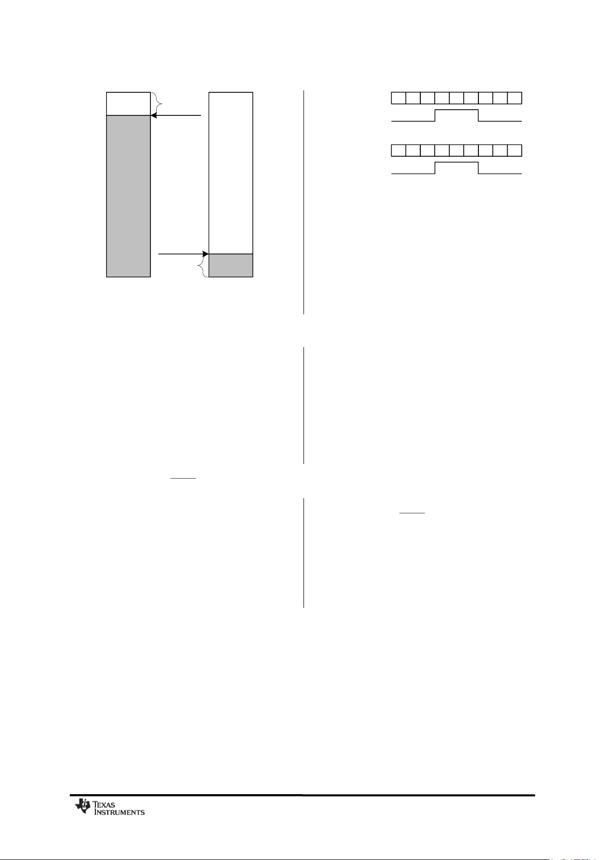
56 bytes
8 bytes
Overflow
margin
Underflow
margin
FIFO_THR=13
FIFO_THR=13
RXFIFO TXFIFO
53 54 55 56 5354555657
6 7 8 9 678910
NUM_RXBYTES
GDO
NUM_TXBYTES
GDO
2_
16
2_256
2
ECHANSPC
XOSC
carrier
MCHANSPCCHANFREQ
f
f
IFFREQ
f
f
XOSC
IF
_
2
10
Figure 30: Number of Bytes in FIFO vs. the
GDO Signal (GDOx_CFG=0x00 in RX and
GDOx_CFG=0x02 in TX, FIFO_THR=13)
CC1101
Figure 29: Example of FIFOs at Threshold
21 Frequency Programming
The frequency programming in
designed to minimize the programming
needed in a channel-oriented system.
To set up a system with channel numbers, the
desired channel spacing is programmed with
the MDMCFG0.CHANSPC_M and
MDMCFG1.CHANSPC_E registers. The channel
spacing registers are mantissa and exponent
respectively. The base or start frequency is set
With a 26 MHz crystal the maximum channel
spacing is 405 kHz. To get e.g. 1 MHz channel
spacing, one solution is to use 333 kHz
channel spacing and select each third channel
in CHANNR.CHAN.
The preferred IF frequency is programmed
with the FSCTRL1.FREQ_IF register. The IF
frequency is given by:
CC1101
is
by the 24 bit frequency word located in the
FREQ2, FREQ1, and FREQ0 registers. This
word will typically be set to the centre of the
lowest channel frequency that is to be used.
The desired channel number is programmed
with the 8-bit channel number register,
CHANNR.CHAN, which is multiplied by the
channel offset. The resultant carrier frequency
is given by:
If any frequency programming register is
altered when the frequency synthesizer is
running, the synthesizer may give an
undesired response. Hence, the frequency
programming should only be updated when
the radio is in the IDLE state.
SWRS061H Page 57 of 98
Page 58

Note: The calibration values are
maintained in SLEEP mode, so the
calibration is still valid after waking up from
SLEEP mode unless supply voltage or
temperature has changed significantly.
22 VCO
The VCO is completely integrated on-chip.
22.1 VCO and PLL Self-Calibration
CC1101
The VCO characteristics vary with temperature
and supply voltage changes as well as the
desired operating frequency. In order to
ensure reliable operation,
frequency synthesizer self-calibration circuitry.
This calibration should be done regularly, and
must be performed after turning on power and
before using a new frequency (or channel).
The number of XOSC cycles for completing
the PLL calibration is given in Table 34 on
page 54.
The calibration can be initiated automatically
or manually. The synthesizer can be
automatically calibrated each time the
synthesizer is turned on, or each time the
synthesizer is turned off automatically. This is
configured with the MCSM0.FS_AUTOCAL
register setting. In manual mode, the
calibration is initiated when the SCAL
command strobe is activated in the IDLE
mode.
CC1101
includes
If calibration is performed each time before
entering active mode (RX or TX) the user can
program register IOCFGx.GDOx_CFG to 0x0A
to check that the PLL is in lock. The lock
detector output available on the GDOx pin
should then be an interrupt for the MCU (x =
0,1, or 2). A positive transition on the GDOx
pin means that the PLL is in lock. As an
alternative the user can read register FSCAL1.
The PLL is in lock if the register content is
different from 0x3F. Refer also to the
Errata Notes [3]. The PLL must be recalibrated until PLL lock is achieved if the PLL
does not lock the first time.
If the calibration is not performed each time
before entering active mode (RX or TX) the
user should program register
IOCFGx.GDOx_CFG to 0x0A to check that the
PLL is in lock before receiving/transmitting
data. The lock detector output available on the
GDOx pin should then be an interrupt for the
MCU (x = 0,1, or 2). A positive transition on
the GDOx pin means that the PLL is in lock.
Since the current calibration values are only
valid for a finite temperature range (typically
±40C) the PLL must be re-calibrated if the lock
indicator does not indicate PLL lock.
CC1101
23 Voltage Regulators
CC1101
contains several on-chip linear voltage
regulators that generate the supply voltages
needed by low-voltage modules. These
voltage regulators are invisible to the user, and
can be viewed as integral parts of the various
modules. The user must however make sure
that the absolute maximum ratings and
required pin voltages in Table 1 and Table 19
are not exceeded.
By setting the CSn pin low, the voltage
regulator to the digital core turns on and the
crystal oscillator starts. The SO pin on the SPI
interface must go low before the first positive
SWRS061H Page 58 of 98
edge of SCLK (setup time is given in Table
22).
If the chip is programmed to enter power-down
mode (SPWD strobe issued), the power will be
turned off after CSn goes high. The power and
crystal oscillator will be turned on again when
CSn goes low.
The voltage regulator for the digital core
requires one external decoupling capacitor.
The voltage regulator output should only be
used for driving the
CC1101
.
Page 59
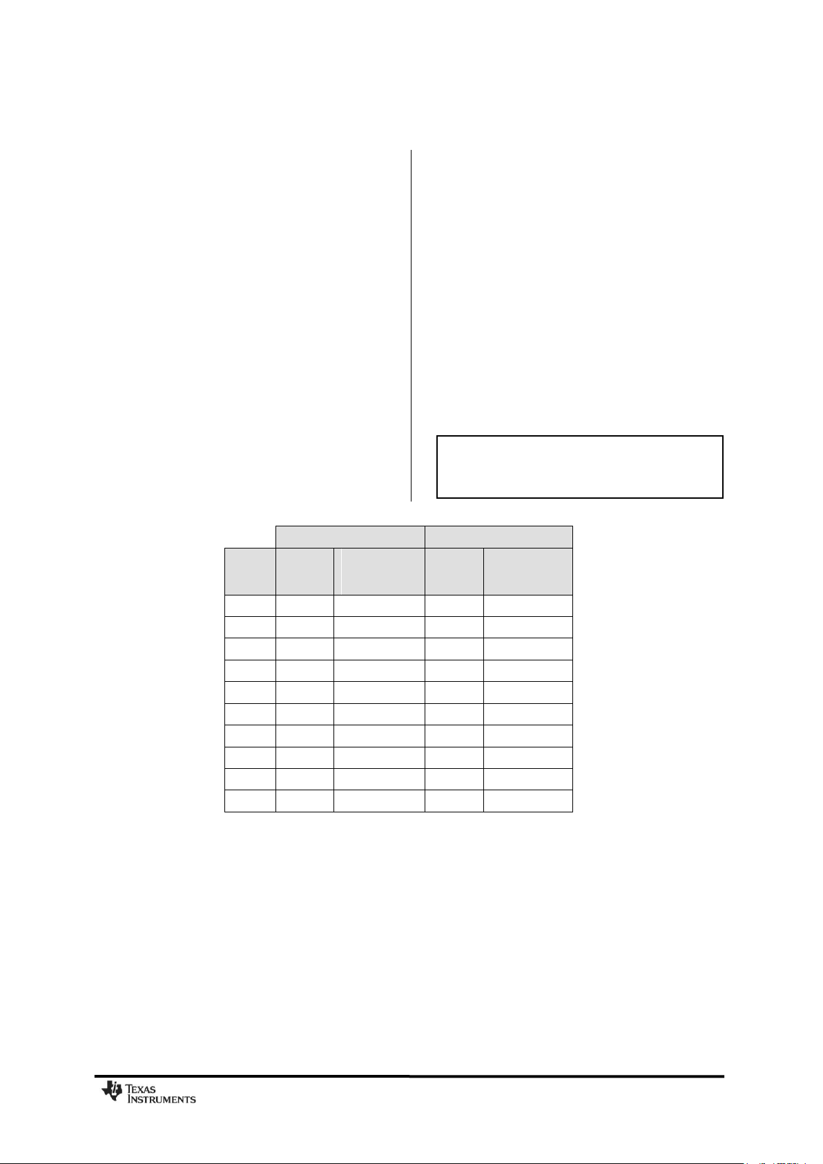
868 MHz
915 MHz
Output
Power
[dBm]
Setting
Current
Consumption,
Typ. [mA]
Setting
Current
Consumption,
Typ. [mA]
-30
0x03
12.0
0x03
11.9
-20
0x17
12.6
0x0E
12.5
-15
0x1D
13.3
0x1E
13.3
-10
0x26
14.5
0x27
14.8
-6
0x37
16.4
0x38
17.0
0
0x50
16.8
0x8E
17.2
5
0x86
19.9
0x84
20.2
7
0xCD
25.8
0xCC
25.7
10
0xC5
30.0
0xC3
30.7
12/11
0xC0
34.2
0xC0
33.4
Note: All content of the PATABLE except
for the first byte (index 0) is lost when
entering the SLEEP state.
24 Output Power Programming
CC1101
The RF output power level from the device has
two levels of programmability as illustrated in
Figure 31. The special PATABLE register can
hold up to eight user selected output power
settings. The 3-bit FREND0.PA_POWER value
selects the PATABLE entry to use. This twolevel functionality provides flexible PA power
ramp up and ramp down at the start and end
of transmission when using 2-FSK, GFSK,
4-FSK, and MSK modulation as well as ASK
modulation shaping. All the PA power settings
in the PATABLE from index 0 up to the
FREND0.PA_POWER value are used.
The power ramping at the start and at the end
of a packet can be turned off by setting
FREND0.PA_POWER=0 and then program the
desired output power to index 0 in the
PATABLE.
If OOK modulation is used, the logic 0 and
logic 1 power levels shall be programmed to
index 0 and 1 respectively.
Table 39 contains recommended PATABLE
settings for various output levels and
frequency bands. DN013 [15] gives the
complete tables for the different frequency
bands using multi-layer inductors. Using PA
settings from 0x61 to 0x6F is not allowed.
Table 40 contains output power and current
consumption for default PATABLE setting
(0xC6).
See Section 10.6 for PATABLE programming
details. PATABLE must be programmed in
burst mode if you want to write to other entries
than PATABLE[0].
Table 37: Optimum PATABLE Settings for Various Output Power Levels and Frequency Bands
Using Wire-Wound Inductors in 868/915 MHz Frequency Bands
SWRS061H Page 59 of 98
Page 60
868 MHz
915 MHz
Default
Power
Setting
Output
Power
[dBm]
Current
Consumption,
Typ. [mA]
Output
Power
[dBm]
Current
Consumption,
Typ. [mA]
0xC6
9.6
29.4
8.9
28.7 315 MHz
433 MHz
868 MHz
915 MHz
Output
Power
[dBm]
Setting
Current
Consumption,
Typ. [mA]
Setting
Current
Consumption,
Typ. [mA]
Setting
Current
Consumption,
Typ. [mA]
Setting
Current
Consumption,
Typ. [mA]
-30
0x12
10.9
0x12
11.9
0x03
12.1
0x03
12.0
-20
0x0D
11.4
0x0E
12.4
0x0F
12.7
0x0E
12.6
-15
0x1C
12.0
0x1D
13.1
0x1E
13.4
0x1E
13.4
-10
0x34
13.5
0x34
14.4
0x27
15.0
0x27
14.9
0
0x51
15.0
0x60
15.9
0x50
16.9
0x8E
16.7
5
0x85
18.3
0x84
19.4
0x81
21.0
0xCD
24.3
7
0xCB
22.1
0xC8
24.2
0xCB
26.8
0xC7
26.9
10
0xC2
26.9
0xC0
29.1
0xC2
32.4
0xC0
31.8
315 MHz
433 MHz
868 MHz
915 MHz
Default
Power
Setting
Output
Power
[dBm]
Current
Consumption,
Typ. [mA]
Output
Power
[dBm]
Current
Consumption,
Typ. [mA]
Output
Power
[dBm]
Current
Consumption,
Typ. [mA]
Output
Power
[dBm]
Current
Consumption,
Typ. [mA]
0xC6
8.5
24.4
7.8
25.2
8.5
29.5
7.2
27.4
CC1101
Table 38: Output Power and Current Consumption for Default PATABLE Setting Using Wire-
Wound Inductors in 868/915 MHz Frequency Bands
Table 39: Optimum PATABLE Settings for Various Output Power Levels and Frequency Bands
Using Multi-layer Inductors
Table 40: Output Power and Current Consumption for Default PATABLE Setting Using Multi-layer
Inductors
25 Shaping and PA Ramping
With ASK modulation, up to eight power
settings are used for shaping. The modulator
contains a counter that counts up when
transmitting a one and down when transmitting
a zero. The counter counts at a rate equal to 8
times the symbol rate. The counter saturates
at FREND0.PA_POWER and 0 respectively.
This counter value is used as an index for a
lookup in the power table. Thus, in order to
utilize the whole table, FREND0.PA_POWER
should be 7 when ASK is active. The shaping
of the ASK signal is dependent on the
configuration of the PATABLE. Figure 32
shows some examples of ASK shaping.
SWRS061H Page 60 of 98
Page 61

e.g 6
PA_POWER[2:0]
in FREND0 register
PATABLE(0)[7:0]
PATABLE(1)[7:0]
PATABLE(2)[7:0]
PATABLE(3)[7:0]
PATABLE(4)[7:0]
PATABLE(5)[7:0]
PATABLE(6)[7:0]
PATABLE(7)[7:0]
Index into PATABLE(7:0)
The PA uses this
setting.
Settings 0 to PA_POWER are
used during ramp-up at start of
transmission and ramp-down at
end of transmission, and for
ASK/OOK modulation.
The SmartRF® Studio software
should be used to obtain optimum
PATABLE settings for various
output powers.
11 0 0 0 1 0
Bit Sequence
1
FREND0.PA_POWER = 3
FREND0.PA_POWER = 7
Time
PATABLE[0]
PATABLE[1]
PATABLE[2]
PATABLE[3]
PATABLE[4]
PATABLE[5]
PATABLE[6]
PATABLE[7]
Output Power
Figure 31: PA_POWER and PATABLE
CC1101
Figure 32: Shaping of ASK Signal
26 General Purpose / Test Output Control Pins
The three digital output pins GDO0, GDO1,
and GDO2 are general control pins configured
with IOCFG0.GDO0_CFG,
IOCFG1.GDO1_CFG, and IOCFG2.GDO2_CFG
respectively. Table 41 shows the different
signals that can be monitored on the GDO
pins. These signals can be used as inputs to
the MCU.
GDO1 is the same pin as the SO pin on the
SPI interface, thus the output programmed on
this pin will only be valid when CSn is high.
The default value for GDO1 is 3-stated which
is useful when the SPI interface is shared with
other devices.
The default value for GDO0 is a 135-141 kHz
clock output (XOSC frequency divided by
192). Since the XOSC is turned on at poweron-reset, this can be used to clock the MCU in
systems with only one crystal. When the MCU
is up and running, it can change the clock
frequency by writing to IOCFG0.GDO0_CFG.
SWRS061H Page 61 of 98
An on-chip analog temperature sensor is
enabled by writing the value 128 (0x80) to the
IOCFG0 register. The voltage on the GDO0
pin is then proportional to temperature. See
Section 4.7 for temperature sensor
specifications.
If the IOCFGx.GDOx_CFG setting is less than
0x20 and IOCFGx_GDOx_INV is 0 (1), the
GDO0 and GDO2 pins will be hardwired to 0
(1), and the GDO1 pin will be hardwired to 1
(0) in the SLEEP state. These signals will be
hardwired until the CHIP_RDYn signal goes
low.
If the IOCFGx.GDOx_CFG setting is 0x20 or
higher, the GDO pins will work as programmed
also in SLEEP state. As an example, GDO1 is
high impedance in all states if
IOCFG1.GDO1_CFG=0x2E.
Page 62
GDOx_CFG[5:0]
Description
0 (0x00)
Associated to the RX FIFO: Asserts when RX FIFO is filled at or above the RX FIFO threshold. De-asserts when RX FIFO
is drained below the same threshold.
1 (0x01)
Associated to the RX FIFO: Asserts when RX FIFO is filled at or above the RX FIFO threshold or the end of packet is
reached. De-asserts when the RX FIFO is empty.
2 (0x02)
Associated to the TX FIFO: Asserts when the TX FIFO is filled at or above the TX FIFO threshold. De-asserts when the TX
FIFO is below the same threshold.
3 (0x03)
Associated to the TX FIFO: Asserts when TX FIFO is full. De-asserts when the TX FIFO is drained below the TX FIFO
threshold.
4 (0x04)
Asserts when the RX FIFO has overflowed. De-asserts when the FIFO has been flushed.
5 (0x05)
Asserts when the TX FIFO has underflowed. De-asserts when the FIFO is flushed.
6 (0x06)
Asserts when sync word has been sent / received, and de-asserts at the end of the packet. In RX, the pin will also deassert when a packet is discarded due to address or maximum length filtering or when the radio enters
RXFIFO_OVERFLOW state. In TX the pin will de-assert if the TX FIFO underflows.
7 (0x07)
Asserts when a packet has been received with CRC OK. De-asserts when the first byte is read from the RX FIFO.
8 (0x08)
Preamble Quality Reached. Asserts when the PQI is above the programmed PQT value. De-asserted when the chip reenters RX state (MARCSTATE=0x0D) or the PQI gets below the programmed PQT value.
9 (0x09)
Clear channel assessment. High when RSSI level is below threshold (dependent on the current CCA_MODE setting).
10 (0x0A)
Lock detector output. The PLL is in lock if the lock detector output has a positive transition or is constantly logic high. To
check for PLL lock the lock detector output should be used as an interrupt for the MCU.
11 (0x0B)
Serial Clock. Synchronous to the data in synchronous serial mode.
In RX mode, data is set up on the falling edge by
CC1101
when GDOx_INV=0.
In TX mode, data is sampled by
CC1101
on the rising edge of the serial clock when GDOx_INV=0.
12 (0x0C)
Serial Synchronous Data Output. Used for synchronous serial mode.
13 (0x0D)
Serial Data Output. Used for asynchronous serial mode.
14 (0x0E)
Carrier sense. High if RSSI level is above threshold. Cleared when entering IDLE mode.
15 (0x0F)
CRC_OK. The last CRC comparison matched. Cleared when entering/restarting RX mode.
16 (0x10)
to
21 (0x15)
Reserved – used for test
22 (0x16)
RX_HARD_DATA[1]. Can be used together with RX_SYMBOL_TICK for alternative serial RX output.
23 (0x17)
RX_HARD_DATA[0]. Can be used together with RX_SYMBOL_TICK for alternative serial RX output.
24 (0x18)
to
26 (0x1A)
Reserved – used for test
27 (0x1B)
PA_PD. Note: PA_PD will have the same signal level in SLEEP and TX states. To control an external PA or RX/TX switch
in applications where the SLEEP state is used it is recommended to use GDOx_CFGx=0x2F instead.
28 (0x1C)
LNA_PD. Note: LNA_PD will have the same signal level in SLEEP and RX states. To control an external LNA or RX/TX
switch in applications where the SLEEP state is used it is recommended to use GDOx_CFGx=0x2F instead.
29 (0x1D)
RX_SYMBOL_TICK. Can be used together with RX_HARD_DATA for alternative serial RX output.
30 (0x1E)
to
35 (0x23)
Reserved – used for test
36 (0x24)
WOR_EVNT0
37 (0x25)
WOR_EVNT1
38 (0x26)
CLK_256
39 (0x27)
CLK_32k
40 (0x28)
Reserved – used for test
41 (0x29)
CHIP_RDYn
42 (0x2A)
Reserved – used for test
43 (0x2B)
XOSC_STABLE
44 (0x2C)
Reserved – used for test
45 (0x2D)
Reserved – used for test
46 (0x2E)
High impedance (3-state)
47 (0x2F)
HW to 0 (HW1 achieved by setting GDOx_INV=1). Can be used to control an external LNA/PA or RX/TX switch.
48 (0x30)
CLK_XOSC/1
Note: There are 3 GDO pins, but only one CLK_XOSC/n can be selected as an output at any
time. If CLK_XOSC/n is to be monitored on one of the GDO pins, the other two GDO pins must
be configured to values less than 0x30. The GDO0 default value is CLK_XOSC/192.
To optimize RF performance, these signals should not be used while the radio is in RX or TX
mode.
49 (0x31)
CLK_XOSC/1.5
50 (0x32)
CLK_XOSC/2
51 (0x33)
CLK_XOSC/3
52 (0x34)
CLK_XOSC/4
53 (0x35)
CLK_XOSC/6
54 (0x36)
CLK_XOSC/8
55 (0x37)
CLK_XOSC/12
56 (0x38)
CLK_XOSC/16
57 (0x39)
CLK_XOSC/24
58 (0x3A)
CLK_XOSC/32
59 (0x3B)
CLK_XOSC/48
60 (0x3C)
CLK_XOSC/64
61 (0x3D)
CLK_XOSC/96
62 (0x3E)
CLK_XOSC/128
63 (0x3F)
CLK_XOSC/192
CC1101
Table 41: GDOx Signal Selection (x = 0, 1, or 2)
SWRS061H Page 62 of 98
Page 63
27 Asynchronous and Synchronous Serial Operation
CC1101
Several features and modes of operation have
been included in the
backward compatibility with previous Chipcon
products and other existing RF communication
systems. For new systems, it is recommended
27.1 Asynchronous Serial Operation
Asynchronous transfer is included in the
CC1101
for backward compatibility with systems
that are already using the asynchronous data
transfer.
When asynchronous transfer is enabled,
several of the support mechanisms for the
MCU that are included in
disabled, such as packet handling hardware,
buffering in the FIFO, and so on. The
asynchronous transfer mode does not allow
for the use of the data whitener, interleaver,
and FEC, and it is not possible to use
Manchester encoding. MSK is not supported
for asynchronous transfer.
Setting PKTCTRL0.PKT_FORMAT to 3
enables asynchronous serial mode. In TX, the
GDO0 pin is used for data input (TX data).
Data output can be on GDO0, GDO1, or
GDO2. This is set by the
IOCFG0.GDO0_CFG, IOCFG1.GDO1_CFG
and IOCFG2.GDO2_CFG fields.
The
CC1101
modulator samples the level of the
asynchronous input 8 times faster than the
programmed data rate. The timing requirement
CC1101
CC1101
to provide
will be
to use the built-in packet handling features, as
they can give more robust communication,
significantly offload the microcontroller, and
simplify software development.
for the asynchronous stream is that the error in
the bit period must be less than one eighth of
the programmed data rate.
In asynchronous serial mode no data decision
is done on-chip and the raw data is put on the
data output line in RX. When using
asynchronous serial mode make sure the
interfacing MCU does proper oversampling
and that it can handle the jitter on the data
output line. The MCU should tolerate a jitter of
±1/8 of a bit period as the data stream is timediscrete using 8 samples per bit.
In asynchronous serial mode there will be
glitches of 37 - 38.5 ns duration (1/XOSC)
occurring infrequently and with random
periods. A simple RC filter can be added to the
data output line between
to get rid of the 37 - 38.5 ns ns glitches if
considered a problem. The filter 3 dB cut-off
frequency needs to be high enough so that the
data is not filtered and at the same time low
enough to remove the glitch. As an example,
for 2.4 kBaud data rate a 1 kohm resistor and
2.7 nF capacitor can be used. This gives a 3
dB cut-off frequency of 59 kHz.
CC1101
and the MCU
27.2 Synchronous Serial Operation
Setting PKTCTRL0.PKT_FORMAT to 1
enables synchronous serial mode. In the
synchronous serial mode, data is transferred
on a two-wire serial interface. The
provides a clock that is used to set up new
data on the data input line or sample data on
the data output line. Data input (TX data) is on
the GDO0 pin. This pin will automatically be
configured as an input when TX is active. The
TX latency is 8 bits. The data output pin can
be any of the GDO pins. This is set by the
IOCFG0.GDO0_CFG, IOCFG1.GDO1_CFG,
and IOCFG2.GDO2_CFG fields. Time from
start of reception until data is available on the
receiver data output pin is equal to 9 bit.
Preamble and sync word insertion/detection
may or may not be active, dependent on the
sync mode set by the MDMCFG2.SYNC_MODE.
SWRS061H Page 63 of 98
CC1101
If preamble and sync word is disabled, all
other packet handler features and FEC should
also be disabled. The MCU must then handle
preamble and sync word insertion and
detection in software.
If preamble and sync word insertion/detection
are left on, all packet handling features and
FEC can be used. One exception is that the
address filtering feature is unavailable in
synchronous serial mode.
When using the packet handling features in
synchronous serial mode, the
and detect the preamble and sync word and
the MCU will only provide/get the data
payload. This is equivalent to the
recommended FIFO operation mode.
An alternative serial RX output option is to
configure any of the GD0 pins for
CC1101
will insert
Page 64
CC1101
RX_SYMBOL_TICK and RX_HARD_DATA, see
Table 41. RX_HARD_DATA[1:0] is the hard
decision symbol. RX_HARD_DATA[1:0]
contain data for 4-ary modulation formats
while RX_HARD_DATA[1] contain data for 2ary modulation formats. The
28 System Considerations and Guidelines
28.1 SRD Regulations
International regulations and national laws
regulate the use of radio receivers and
transmitters. Short Range Devices (SRDs) for
license free operation below 1 GHz are usually
operated in the 315 MHz, 433 MHz, 868 MHz
or 915 MHz frequency bands. The
specifically designed for such use with its 300
- 348 MHz, 387 - 464 MHz, and 779 - 928
MHz operating ranges. The most important
regulations when using the
MHz, 433 MHz, 868 MHz, or 915 MHz
frequency bands are EN 300 220 (Europe)
and FCC CFR47 Part 15 (USA).
CC1101
CC1101
is
in the 315
RX_SYMBOL_TICK signal is the symbol clock
and is high for one half symbol period
whenever a new symbol is presented on the
hard and soft data outputs. This option may be
used for both synchronous and asynchronous
interfaces.
For compliance with modulation bandwidth
requirements under EN 300 220 in the 863 to
870 MHz frequency range it is recommended
to use a 26 MHz crystal for frequencies below
869 MHz and a 27 MHz crystal for frequencies
above 869 MHz.
Please note that compliance with regulations
is dependent on the complete system
performance. It is the customer‟s responsibility
to ensure that the system complies with
regulations.
28.2 Frequency Hopping and Multi-Channel Systems
The 315 MHz, 433 MHz, 868 MHz, or 915
MHz bands are shared by many systems both
in industrial, office, and home environments. It
is therefore recommended to use frequency
hopping spread spectrum (FHSS) or a multichannel protocol because the frequency
diversity makes the system more robust with
respect to interference from other systems
operating in the same frequency band. FHSS
also combats multipath fading.
CC1101
is highly suited for FHSS or multichannel systems due to its agile frequency
synthesizer and effective communication
interface. Using the packet handling support
and data buffering is also beneficial in such
systems as these features will significantly
offload the host controller.
Charge pump current, VCO current, and VCO
capacitance array calibration data is required
for each frequency when implementing
frequency hopping for
ways of obtaining the calibration data from the
chip:
1) Frequency hopping with calibration for each
hop. The PLL calibration time is 712/724 µs
(26 MHz crystal and TEST0 = 0x09/0B, see
Table 35). The blanking interval between each
frequency hop is then 787/799 µs.
CC1101
. There are 3
2) Fast frequency hopping without calibration
for each hop can be done by performing the
necessary calibrating at startup and saving the
resulting FSCAL3, FSCAL2, and FSCAL1
register values in MCU memory. The VCO
capacitance calibration FSCAL1 register value
must be found for each RF frequency to be
used. The VCO current calibration value and
the charge pump current calibration value
available in FSCAL2 and FSCAL3 respectively
are not dependent on the RF frequency, so the
same value can therefore be used for all RF
frequencies for these two registers. Between
each frequency hop, the calibration process
can then be replaced by writing the FSCAL3,
FSCAL2 and FSCAL1 register values that
corresponds to the next RF frequency. The
PLL turn on time is approximately 75 µs (Table
34). The blanking interval between each
frequency hop is then approximately 75 µs.
3) Run calibration on a single frequency at
startup. Next write 0 to FSCAL3[5:4] to
disable the charge pump calibration. After
writing to FSCAL3[5:4], strobe SRX (or STX)
with MCSM0.FS_AUTOCAL=1 for each new
frequency hop. That is, VCO current and VCO
capacitance calibration is done, but not charge
pump current calibration. When charge pump
current calibration is disabled the calibration
SWRS061H Page 64 of 98
Page 65

Note: The content in the TEST0 register is
not retained in SLEEP state, thus it is
necessary to re-write this register when
returning from the SLEEP state.
Note: The sensitivity and thus transmission
range is reduced for high data rate bursts
compared to lower data rates.
CC1101
time is reduced from 712/724 µs to 145/157 µs
(26 MHz crystal and TEST0 = 0x09/0B, see
Table 35). The blanking interval between each
frequency hop is then 220/232 µs.
There is a trade off between blanking time and
memory space needed for storing calibration
data in non-volatile memory. Solution 2) above
gives the shortest blanking interval, but
requires more memory space to store
calibration values. This solution also requires
that the supply voltage and temperature do not
vary much in order to have a robust solution.
Solution 3) gives 567 µs smaller blanking
interval than solution 1).
28.3 Wideband Modulation when not Using Spread Spectrum
Digital modulation systems under FCC Section
15.247 include 2-FSK, GFSK, and 4-FSK
modulation. A maximum peak output power of
1 W (+30 dBm) is allowed if the 6 dB
bandwidth of the modulated signal exceeds
500 kHz. In addition, the peak power spectral
density conducted to the antenna shall not be
greater than +8 dBm in any 3 kHz band.
Operating at high data rates and frequency
separation, the
CC1101
is suited for systems
The recommended settings for
TEST0.VCO_SEL_CAL_EN change with
frequency. This means that one should always
use SmartRF Studio [5] to get the correct
settings for a specific frequency before doing a
calibration, regardless of which calibration
method is being used.
targeting compliance with digital modulation
system as defined by FCC Section 15.247. An
external power amplifier such as
needed to increase the output above +11
dBm. Please refer to DN006 [11] for further
details concerning wideband modulation using
CC1101
600 kbps data rate, +19 dBm output power
when using
and DN036 for wideband modulation at
CC1101 +CC1101
[25].
CC1190
[21] is
28.4 Wireless MBUS
The wireless MBUS standard is a
communication standard for meters and
wireless readout of meters, and specifies the
physical and the data link layer. Power
consumption is a critical parameter for the
meter side, since the communication link shall
be operative for the full lifetime of the meter,
without changing the battery.
with
MSP430
Wireless MBUS standard,
28.5 Data Burst Transmissions
The high maximum data rate of
up for burst transmissions. A low average data
rate link (e.g. 10 kBaud) can be realized by
using a higher over-the-air data rate. Buffering
the data and transmitting in bursts at high data
rate (e.g. 500 kBaud) will reduce the time in
active mode, and hence also reduce the
average current consumption significantly.
28.6 Continuous Transmissions
is an excellent choice for the
CC1101
CC1101
is a truly low
combined
CC1101
opens
cost, low power and flexible transceiver, and
MSP430
MCU. For more informati on regarding using
CC1101
AN067 [14].
Since the Wireless MBUS standard operates
in the 868-870 ISM band, the radio
requirements must also comply with the ETSI
EN 300 220 and CEPT/ERC/REC 70-03 E
standards.
Reducing the time in active mode will reduce
the likelihood of collisions with other systems
in the same frequency range.
a high performance and low power
for Wireless MBUS applications, see
In data streaming applications, the
opens up for continuous transmissions at 500
kBaud effective data rate. As the modulation is
SWRS061H Page 65 of 98
CC1101
done with a closed loop PLL, there is no
limitation in the length of a transmission (open
loop modulation used in some transceivers
Page 66
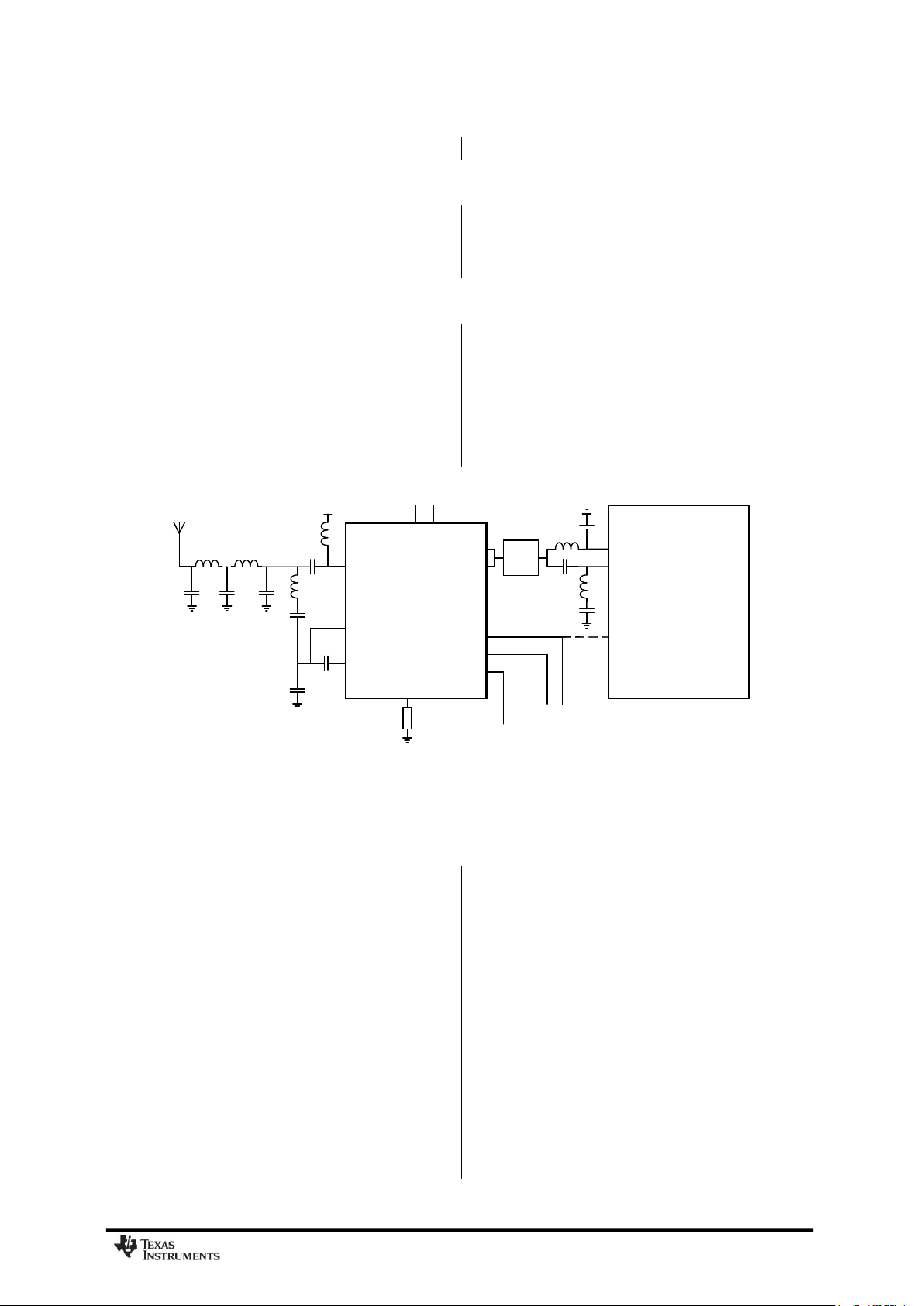
CC1101
Connected to
VDD / GND / MCU
RF _ P
GDOx
RF _ N
SAW
CC
1190
PA _ EN
LNA _ EN
HGM B I A S
VDD
TR _ SW
LNA _ OUT
PA _ OUT
PA _ IN
LNA _ IN
V D D
_
L
N A V
D
D
_
P A 1 V D
D _ P
A 2 VDD
Connected to MCU
CC1101
often prevents this kind of continuous data streaming and reduces the effective data rate).
28.7 Battery Operated Systems
In low power applications, the SLEEP state
with the crystal oscillator core switched off
should be used when the
CC1101
is not active.
It is possible to leave the crystal oscillator core
28.8 Increasing Range
In some applications it may be necessary to
extend the range. The
CC1190
[21] is a range
extender for 850-950 MHz RF transceivers,
transmitters, and System-on-Chip devices
from Texas Instruments. It increases the link
budget by providing a power amplifier (PA) for
increased output power, and a low-noise
amplifier (LNA) with low noise figure for
running in the SLEEP state if start-up time is
critical. The WOR functionality should be used
in low power applications.
improved receiver sensitivity in addition to
switches and RF matching for simple design of
high performance wireless systems. Refer to
AN094 [22] and AN096 [23] for performance
figures of the
CC1101 + CC1190
combination.
Figure 33 shows a simplified application
circuit.
Figure 33: Simplified CC1101-CC1190 Application Circuit
29 Configuration Registers
The configuration of
programming 8-bit registers. The optimum
configuration data based on selected system
parameters are most easily found by using the
SmartRF Studio software [5]. Complete
descriptions of the registers are given in the
following tables. After chip reset, all the
registers have default values as shown in the
tables. The optimum register setting might
differ from the default value. After a reset, all
registers that shall be different from the default
value therefore needs to be programmed
through the SPI interface.
There are 13 command strobe registers, listed
in Table 42. Accessing these registers will
initiate the change of an internal state or
mode. There are 47 normal 8-bit configuration
CC1101
is done by
registers listed in Table 43. Many of these
registers are for test purposes only, and need
not be written for normal operation of
CC1101
.
There are also 12 status registers that are
listed in Table 44. These registers, which are
read-only, contain information about the status
of
CC1101
.
The two FIFOs are accessed through one 8-bit
register. Write operations write to the TX FIFO,
while read operations read from the RX FIFO.
During the header byte transfer and while
writing data to a register or the TX FIFO, a
status byte is returned on the SO line. This
status byte is described in Table 23 on page
31.
SWRS061H Page 66 of 98
Page 67

Address
Strobe
Name
Description
0x30
SRES
Reset chip.
0x31
SFSTXON
Enable and calibrate frequency synthesizer (if MCSM0.FS_AUTOCAL=1). If in RX (with CCA):
Go to a wait state where only the synthesizer is running (for quick RX / TX turnaround).
0x32
SXOFF
Turn off crystal oscillator.
0x33
SCAL
Calibrate frequency synthesizer and turn it off. SCAL can be strobed from IDLE mode without
setting manual calibration mode (MCSM0.FS_AUTOCAL=0)
0x34
SRX
Enable RX. Perform calibration first if coming from IDLE and MCSM0.FS_AUTOCAL=1.
0x35
STX
In IDLE state: Enable TX. Perform calibration first if MCSM0.FS_AUTOCAL=1.
If in RX state and CCA is enabled: Only go to TX if channel is clear.
0x36
SIDLE
Exit RX / TX, turn off frequency synthesizer and exit Wake-On-Radio mode if applicable.
0x38
SWOR
Start automatic RX polling sequence (Wake-on-Radio) as described in Section 19.5 if
WORCTRL.RC_PD=0.
0x39
SPWD
Enter power down mode when CSn goes high.
0x3A
SFRX
Flush the RX FIFO buffer. Only issue SFRX in IDLE or RXFIFO_OVERFLOW states.
0x3B
SFTX
Flush the TX FIFO buffer. Only issue SFTX in IDLE or TXFIFO_UNDERFLOW states.
0x3C
SWORRST
Reset real time clock to Event1 value.
0x3D
SNOP
No operation. May be used to get access to the chip status byte.
CC1101
Table 45 summarizes the SPI address space.
The address to use is given by adding the
base address to the left and the burst and
read/write bits on the top. Note that the burst
bit has different meaning for base addresses
above and below 0x2F.
Table 42: Command Strobes
SWRS061H Page 67 of 98
Page 68
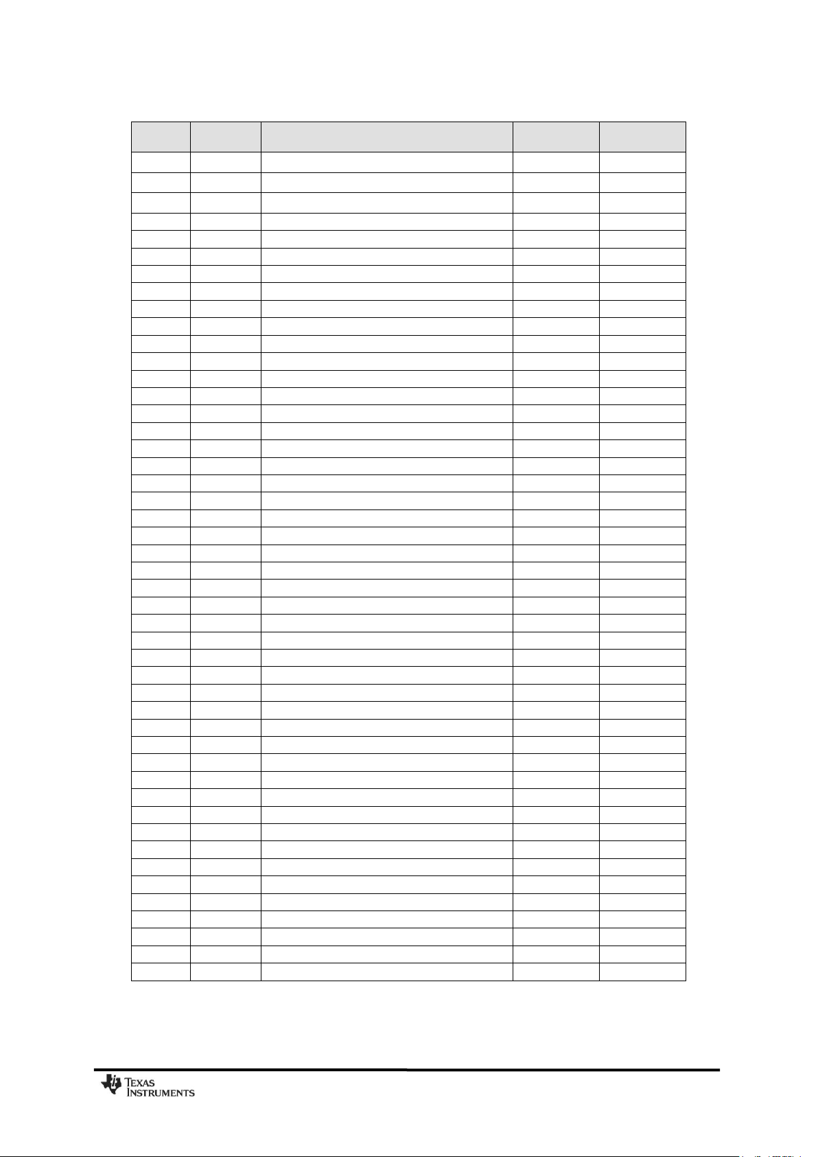
Address
Register
Description
Preserved in
SLEEP State
Details on
Page Number
0x00
IOCFG2
GDO2 output pin configuration
Yes
71
0x01
IOCFG1
GDO1 output pin configuration
Yes
71
0x02
IOCFG0
GDO0 output pin configuration
Yes
71
0x03
FIFOTHR
RX FIFO and TX FIFO thresholds
Yes
72
0x04
SYNC1
Sync word, high byte
Yes
73
0x05
SYNC0
Sync word, low byte
Yes
73
0x06
PKTLEN
Packet length
Yes
73
0x07
PKTCTRL1
Packet automation control
Yes
73
0x08
PKTCTRL0
Packet automation control
Yes
74
0x09
ADDR
Device address
Yes
74
0x0A
CHANNR
Channel number
Yes
74
0x0B
FSCTRL1
Frequency synthesizer control
Yes
75
0x0C
FSCTRL0
Frequency synthesizer control
Yes
75
0x0D
FREQ2
Frequency control word, high byte
Yes
75
0x0E
FREQ1
Frequency control word, middle byte
Yes
75
0x0F
FREQ0
Frequency control word, low byte
Yes
75
0x10
MDMCFG4
Modem configuration
Yes
76
0x11
MDMCFG3
Modem configuration
Yes
76
0x12
MDMCFG2
Modem configuration
Yes
77
0x13
MDMCFG1
Modem configuration
Yes
78
0x14
MDMCFG0
Modem configuration
Yes
78
0x15
DEVIATN
Modem deviation setting
Yes
79
0x16
MCSM2
Main Radio Control State Machine configuration
Yes
80
0x17
MCSM1
Main Radio Control State Machine configuration
Yes
81
0x18
MCSM0
Main Radio Control State Machine configuration
Yes
82
0x19
FOCCFG
Frequency Offset Compensation configuration
Yes
83
0x1A
BSCFG
Bit Synchronization configuration
Yes
84
0x1B
AGCTRL2
AGC control
Yes
85
0x1C
AGCTRL1
AGC control
Yes
86
0x1D
AGCTRL0
AGC control
Yes
87
0x1E
WOREVT1
High byte Event 0 timeout
Yes
87
0x1F
WOREVT0
Low byte Event 0 timeout
Yes
88
0x20
WORCTRL
Wake On Radio control
Yes
88
0x21
FREND1
Front end RX configuration
Yes
89
0x22
FREND0
Front end TX configuration
Yes
89
0x23
FSCAL3
Frequency synthesizer calibration
Yes
89
0x24
FSCAL2
Frequency synthesizer calibration
Yes
90
0x25
FSCAL1
Frequency synthesizer calibration
Yes
90
0x26
FSCAL0
Frequency synthesizer calibration
Yes
90
0x27
RCCTRL1
RC oscillator configuration
Yes
90
0x28
RCCTRL0
RC oscillator configuration
Yes
90
0x29
FSTEST
Frequency synthesizer calibration control
No
91
0x2A
PTEST
Production test
No
91
0x2B
AGCTEST
AGC test
No
91
0x2C
TEST2
Various test settings
No
91
0x2D
TEST1
Various test settings
No
91
0x2E
TEST0
Various test settings
No
92
CC1101
SWRS061H Page 68 of 98
Table 43: Configuration Registers Overview
Page 69

Address
Register
Description
Details on page number
0x30 (0xF0)
PARTNUM
Part number for
CC1101
92
0x31 (0xF1)
VERSION
Current version number
92
0x32 (0xF2)
FREQEST
Frequency Offset Estimate
92
0x33 (0xF3)
LQI
Demodulator estimate for Link Quality
92
0x34 (0xF4)
RSSI
Received signal strength indication
92
0x35 (0xF5)
MARCSTATE
Control state machine state
93
0x36 (0xF6)
WORTIME1
High byte of WOR timer
93
0x37 (0xF7)
WORTIME0
Low byte of WOR timer
93
0x38 (0xF8)
PKTSTATUS
Current GDOx status and packet status
94
0x39 (0xF9)
VCO_VC_DAC
Current setting from PLL calibration
module
94
0x3A (0xFA)
TXBYTES
Underflow and number of bytes in the TX
FIFO
94
0x3B (0xFB)
RXBYTES
Overflow and number of bytes in the RX
FIFO
94
0x3C (0xFC)
RCCTRL1_STATUS
Last RC oscillator calibration result
94
0x3D (0xFD)
RCCTRL0_STATUS
Last RC oscillator calibration result
95
CC1101
Table 44: Status Registers Overview
Table 45: SPI Address Space (see next page)
SWRS061H Page 69 of 98
Page 70
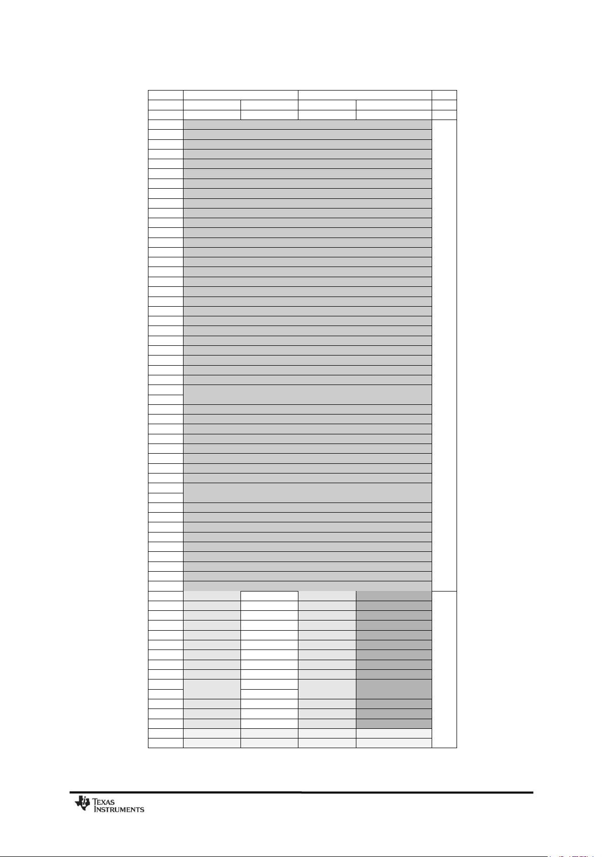
Write
Read
Single Byte
Burst
Single Byte
Burst
+0x00
+0x40
+0x80
+0xC0
0x00
IOCFG2
R/W configuration registers, burst access possible
0x01
IOCFG1
0x02
IOCFG0
0x03
FIFOTHR
0x04
SYNC1
0x05
SYNC0
0x06
PKTLEN
0x07
PKTCTRL1
0x08
PKTCTRL0
0x09
ADDR
0x0A
CHANNR
0x0B
FSCTRL1
0x0C
FSCTRL0
0x0D
FREQ2
0x0E
FREQ1
0x0F
FREQ0
0x10
MDMCFG4
0x11
MDMCFG3
0x12
MDMCFG2
0x13
MDMCFG1
0x14
MDMCFG0
0x15
DEVIATN
0x16
MCSM2
0x17
MCSM1
0x18
MCSM0
0x19
FOCCFG
0x1A
BSCFG
0x1B
AGCCTRL2
0x1C
AGCCTRL1
0x1D
AGCCTRL0
0x1E
WOREVT1
0x1F
WOREVT0
0x20
WORCTRL
0x21
FREND1
0x22
FREND0
0x23
FSCAL3
0x24
FSCAL2
0x25
FSCAL1
0x26
FSCAL0
0x27
RCCTRL1
0x28
RCCTRL0
0x29
FSTEST
0x2A
PTEST
0x2B
AGCTEST
0x2C
TEST2
0x2D
TEST1
0x2E
TEST0
0x2F 0x30
SRES
SRES
PARTNUM
Command Strobes, Status registers
(read only) and multi byte registers
0x31
SFSTXON
SFSTXON
VERSION
0x32
SXOFF
SXOFF
FREQEST
0x33
SCAL
SCAL
LQI
0x34
SRX SRX
RSSI
0x35
STX STX
MARCSTATE
0x36
SIDLE
SIDLE
WORTIME1
0x37 WORTIME0
0x38
SWOR
SWOR
PKTSTATUS
0x39
SPWD
SPWD
VCO_VC_DAC
0x3A
SFRX
SFRX
TXBYTES
0x3B
SFTX
SFTX
RXBYTES
0x3C
SWORRST
SWORRST
RCCTRL1_STATUS
0x3D
SNOP
SNOP
RCCTRL0_STATUS
0x3E
PATABLE
PATABLE
PATABLE
PATABLE
0x3F
TX FIFO
TX FIFO
RX FIFO
RX FIFO
CC1101
SWRS061H Page 70 of 98
Page 71
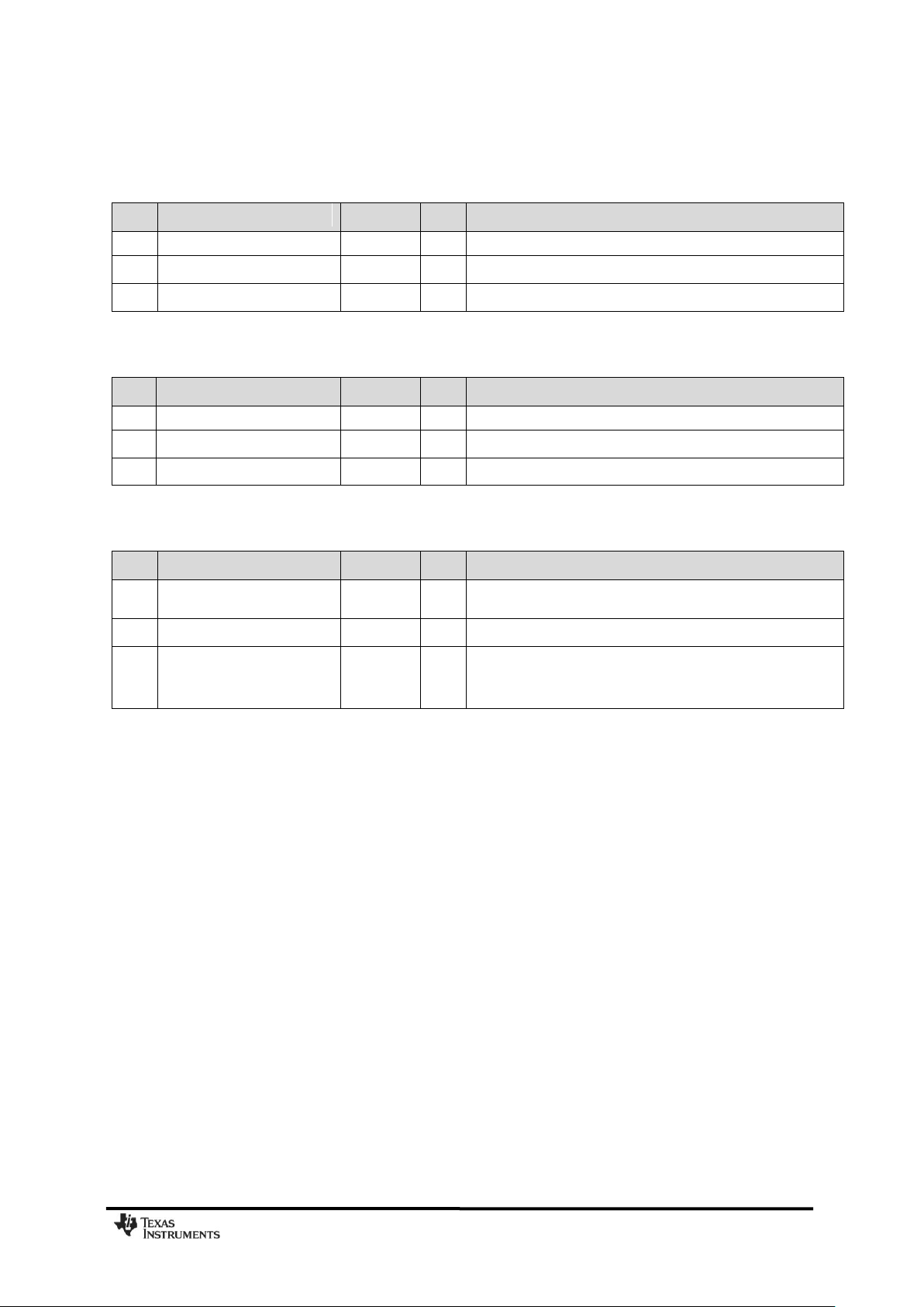
Bit
Field Name
Reset
R/W
Description
7
R0
Not used
6
GDO2_INV
0
R/W
Invert output, i.e. select active low (1) / high (0)
5:0
GDO2_CFG[5:0]
41 (0x29)
R/W
Default is CHP_RDYn (See Table 41 on page 62).
Bit
Field Name
Reset
R/W
Description
7
GDO_DS
0
R/W
Set high (1) or low (0) output drive strength on the GDO pins.
6
GDO1_INV
0
R/W
Invert output, i.e. select active low (1) / high (0)
5:0
GDO1_CFG[5:0]
46 (0x2E)
R/W
Default is 3-state (See Table 41 on page 62).
Bit
Field Name
Reset
R/W
Description
7
TEMP_SENSOR_ENABLE
0
R/W
Enable analog temperature sensor. Write 0 in all other register
bits when using temperature sensor.
6
GDO0_INV
0
R/W
Invert output, i.e. select active low (1) / high (0)
5:0
GDO0_CFG[5:0]
63 (0x3F)
R/W
Default is CLK_XOSC/192 (See Table 41 on page 62).
It is recommended to disable the clock output in initialization, in
order to optimize RF performance.
CC1101
29.1 Configuration Register Details – Registers with preserved values in SLEEP state
0x00: IOCFG2 – GDO2 Output Pin Configuration
0x01: IOCFG1 – GDO1 Output Pin Configuration
0x02: IOCFG0 – GDO0 Output Pin Configuration
SWRS061H Page 71 of 98
Page 72
Bit
Field Name
Reset
R/W
Description
7 0
R/W
Reserved , write 0 for compatibility with possible future extensions
6
ADC_RETENTION
0
R/W
0: TEST1 = 0x31 and TEST2= 0x88 when waking up from SLEEP
1: TEST1 = 0x35 and TEST2 = 0x81 when waking up from SLEEP
Note that the changes in the TEST registers due to the
ADC_RETENTION bit setting are only seen INTERNALLY in the analog
part. The values read from the TEST registers when waking up from
SLEEP mode will always be the reset value.
The ADC_RETENTION bit should be set to 1before going into SLEEP
mode if settings with an RX filter bandwidth below 325 kHz are wanted at
time of wake-up.
5:4
CLOSE_IN_RX [1:0]
0 (00)
R/W
For more details, please see DN010 [8]
Setting
RX Attenuation, Typical Values
0 (00)
0 dB
1 (01)
6 dB
2 (10)
12 dB
3 (11)
18 dB
3:0
FIFO_THR[3:0]
7 (0111)
R/W
Set the threshold for the TX FIFO and RX FIFO. The threshold is
exceeded when the number of bytes in the FIFO is equal to or higher than
the threshold value.
Setting
Bytes in TX FIFO
Bytes in RX FIFO
0 (0000)
61
4
1 (0001)
57
8
2 (0010)
53
12
3 (0011)
49
16
4 (0100)
45
20
5 (0101)
41
24
6 (0110)
37
28
7 (0111)
33
32
8 (1000)
29
36
9 (1001)
25
40
10 (1010)
21
44
11 (1011)
17
48
12 (1100)
13
52
13 (1101) 9 56
14 (1110) 5 60
15 (1111) 1 64
0x03: FIFOTHR – RX FIFO and TX FIFO Thresholds
CC1101
SWRS061H Page 72 of 98
Page 73
Bit
Field Name
Reset
R/W
Description
7:0
SYNC[15:8]
211 (0xD3)
R/W
8 MSB of 16-bit sync word
Bit
Field Name
Reset
R/W
Description
7:0
SYNC[7:0]
145 (0x91)
R/W
8 LSB of 16-bit sync word
Bit
Field Name
Reset
R/W
Description
7:0
PACKET_LENGTH
255 (0xFF)
R/W
Indicates the packet length when fixed packet length mode is enabled. If
variable packet length mode is used, this value indicates the maximum
packet length allowed. This value must be different from 0.
Bit
Field Name
Reset
R/W
Description
7:5
PQT[2:0]
0 (0x00)
R/W
Preamble quality estimator threshold. The preamble quality estimator
increases an internal counter by one each time a bit is received that is
different from the previous bit, and decreases the counter by 8 each time a
bit is received that is the same as the last bit.
A threshold of 4∙PQT for this counter is used to gate sync word detection.
When PQT=0 a sync word is always accepted.
4 0
R0
Not Used.
3
CRC_AUTOFLUSH
0
R/W
Enable automatic flush of RX FIFO when CRC is not OK. This requires that
only one packet is in the RXIFIFO and that packet length is limited to the
RX FIFO size.
2
APPEND_STATUS
1
R/W
When enabled, two status bytes will be appended to the payload of the
packet. The status bytes contain RSSI and LQI values, as well as CRC OK.
1:0
ADR_CHK[1:0]
0 (00)
R/W
Controls address check configuration of received packages.
Setting
Address check configuration
0 (00)
No address check
1 (01)
Address check, no broadcast
2 (10)
Address check and 0 (0x00) broadcast
3 (11)
Address check and 0 (0x00) and 255 (0xFF)
broadcast
0x04: SYNC1 – Sync Word, High Byte
0x05: SYNC0 – Sync Word, Low Byte
0x06: PKTLEN – Packet Length
0x07: PKTCTRL1 – Packet Automation Control
CC1101
SWRS061H Page 73 of 98
Page 74

Bit
Field Name
Reset
R/W
Description
7
R0
Not used
6
WHITE_DATA
1
R/W
Turn data whitening on / off
0: Whitening off
1: Whitening on
5:4
PKT_FORMAT[1:0]
0 (00)
R/W
Format of RX and TX data
Setting
Packet format
0 (00)
Normal mode, use FIFOs for RX and TX
1 (01)
Synchronous serial mode, Data in on GDO0 and
data out on either of the GDOx pins
2 (10)
Random TX mode; sends random data using PN9
generator. Used for test.
Works as normal mode, setting 0 (00), in RX
3 (11)
Asynchronous serial mode, Data in on GDO0 and
data out on either of the GDOx pins
3 0
R0
Not used
2
CRC_EN
1
R/W
1: CRC calculation in TX and CRC check in RX enabled
0: CRC disabled for TX and RX
1:0
LENGTH_CONFIG[1:0]
1 (01)
R/W
Configure the packet length
Setting
Packet length configuration
0 (00)
Fixed packet length mode. Length configured in
PKTLEN register
1 (01)
Variable packet length mode. Packet length
configured by the first byte after sync word
2 (10)
Infinite packet length mode
3 (11)
Reserved
Bit
Field Name
Reset
R/W
Description
7:0
DEVICE_ADDR[7:0]
0 (0x00)
R/W
Address used for packet filtration. Optional broadcast addresses are 0
(0x00) and 255 (0xFF).
Bit
Field Name
Reset
R/W
Description
7:0
CHAN[7:0]
0 (0x00)
R/W
The 8-bit unsigned channel number, which is multiplied by the channel
spacing setting and added to the base frequency.
0x08: PKTCTRL0 – Packet Automation Control
CC1101
0x09: ADDR – Device Address
0x0A: CHANNR – Channel Number
SWRS061H Page 74 of 98
Page 75
Bit
Field Name
Reset
R/W
Description
7:6
R0
Not used
5 0
R/W
Reserved
4:0
FREQ_IF[4:0]
15 (0x0F)
R/W
The desired IF frequency to employ in RX. Subtracted from FS base frequency
in RX and controls the digital complex mixer in the demodulator.
IFFREQ
f
f
XOSC
IF
_
2
10
The default value gives an IF frequency of 381kHz, assuming a 26.0 MHz
crystal.
Bit
Field Name
Reset
R/W
Description
7:0
FREQOFF[7:0]
0 (0x00)
R/W
Frequency offset added to the base frequency before being used by the
frequency synthesizer. (2s-complement).
Resolution is F
XTAL
/214 (1.59kHz-1.65kHz); range is ±202 kHz to ±210 kHz,
dependent of XTAL frequency.
Bit
Field Name
Reset
R/W
Description
7:6
FREQ[23:22]
0 (00)
R
FREQ[23:22] is always 0 (the FREQ2 register is less than 36 with 26-27 MHz
crystal)
5:0
FREQ[21:16]
30 (0x1E)
R/W
FREQ[23:0] is the base frequency for the frequency synthesiser in
increments of f
XOSC
/216.
0:23
2
16
FREQ
f
f
XOSC
carrier
Bit
Field Name
Reset
R/W
Description
7:0
FREQ[15:8]
196 (0xC4)
R/W
Ref. FREQ2 register
Bit
Field Name
Reset
R/W
Description
7:0
FREQ[7:0]
236 (0xEC)
R/W
Ref. FREQ2 register
0x0B: FSCTRL1 – Frequency Synthesizer Control
0x0C: FSCTRL0 – Frequency Synthesizer Control
CC1101
0x0D: FREQ2 – Frequency Control Word, High Byte
0x0E: FREQ1 – Frequency Control Word, Middle Byte
0x0F: FREQ0 – Frequency Control Word, Low Byte
SWRS061H Page 75 of 98
Page 76

Bit
Field Name
Reset
R/W
Description
7:6
CHANBW_E[1:0]
2 (0x02)
R/W
5:4
CHANBW_M[1:0]
0 (0x00)
R/W
Sets the decimation ratio for the delta-sigma ADC input stream and thus the
channel bandwidth.
ECHANBW
XOSC
channel
MCHANBW
f
BW
_
2)·_4(8
The default values give 203 kHz channel filter bandwidth, assuming a 26.0
MHz crystal.
3:0
DRATE_E[3:0]
12 (0x0C)
R/W
The exponent of the user specified symbol rate
Bit
Field Name
Reset
R/W
Description
7:0
DRATE_M[7:0]
34 (0x22)
R/W
The mantissa of the user specified symbol rate. The symbol rate is configured
using an unsigned, floating-point number with 9-bit mantissa and 4-bit
exponent. The 9th bit is a hidden „1‟. The resulting data rate is:
XOSC
EDRATE
DATA
f
MDRATE
R
28
_
2
2_256
The default values give a data rate of 115.051 kBaud (closest setting to 115.2
kBaud), assuming a 26.0 MHz crystal.
0x10: MDMCFG4 – Modem Configuration
0x11: MDMCFG3 – Modem Configuration
CC1101
SWRS061H Page 76 of 98
Page 77
Bit
Field Name
Reset
R/W
Description
7
DEM_DCFILT_OFF
0
R/W
Disable digital DC blocking filter before demodulator.
0 = Enable (better sensitivity)
1 = Disable (current optimized). Only for data rates
≤ 250 kBaud
The recommended IF frequency changes when the DC blocking is disabled.
Please use SmartRF Studio [5] to calculate correct register setting.
6:4
MOD_FORMAT[2:0]
0 (000)
R/W
The modulation format of the radio signal
Setting
Modulation format
0 (000)
2-FSK
1 (001)
GFSK
2 (010)
-
3 (011)
ASK/OOK
4 (100)
4-FSK
5 (101)
-
6 (110)
-
7 (111)
MSK
MSK is only supported for data rates above 26 kBaud
3
MANCHESTER_EN
0
R/W
Enables Manchester encoding/decoding.
0 = Disable
1 = Enable
2:0
SYNC_MODE[2:0]
2 (010)
R/W
Combined sync-word qualifier mode.
The values 0 (000) and 4 (100) disables preamble and sync word
transmission in TX and preamble and sync word detection in RX.
The values 1 (001), 2 (010), 5 (101) and 6 (110) enables 16-bit sync word
transmission in TX and 16-bits sync word detection in RX. Only 15 of 16 bits
need to match in RX when using setting 1 (001) or 5 (101). The values 3 (011)
and 7 (111) enables repeated sync word transmission in TX and 32-bits sync
word detection in RX (only 30 of 32 bits need to match).
Setting
Sync-word qualifier mode
0 (000)
No preamble/sync
1 (001)
15/16 sync word bits detected
2 (010)
16/16 sync word bits detected
3 (011)
30/32 sync word bits detected
4 (100)
No preamble/sync, carrier-sense
above threshold
5 (101)
15/16 + carrier-sense above threshold
6 (110)
16/16 + carrier-sense above threshold
7 (111)
30/32 + carrier-sense above threshold
0x12: MDMCFG2 – Modem Configuration
CC1101
SWRS061H Page 77 of 98
Page 78

Bit
Field Name
Reset
R/W
Description
7
FEC_EN
0
R/W
Enable Forward Error Correction (FEC) with interleaving for packet
payload
0 = Disable
1 = Enable (Only supported for fixed packet length mode, i.e.
PKTCTRL0.LENGTH_CONFIG=0)
6:4
NUM_PREAMBLE[2:0]
2 (010)
R/W
Sets the minimum number of preamble bytes to be transmitted
Setting
Number of preamble bytes
0 (000)
2
1 (001)
3
2 (010)
4
3 (011)
6
4 (100)
8
5 (101)
12
6 (110)
16
7 (111)
24 3:2
R0
Not used
1:0
CHANSPC_E[1:0]
2 (10)
R/W
2 bit exponent of channel spacing
Bit
Field Name
Reset
R/W
Description
7:0
CHANSPC_M[7:0]
248 (0xF8)
R/W
8-bit mantissa of channel spacing. The channel spacing is
multiplied by the channel number CHAN and added to the base
frequency. It is unsigned and has the format:
ECHANSPC
XOSC
CHANNEL
MCHANSPC
f
f
_
18
2_256
2
The default values give 199.951 kHz channel spacing (the closest
setting to 200 kHz), assuming 26.0 MHz crystal frequency.
0x13: MDMCFG1– Modem Configuration
CC1101
0x14: MDMCFG0– Modem Configuration
SWRS061H Page 78 of 98
Page 79

Bit
Field Name
Reset
R/W
Description
7
R0
Not used.
6:4
DEVIATION_E[2:0]
4 (100)
R/W
Deviation exponent.
3
R0
Not used.
2:0
DEVIATION_M[2:0]
7 (111)
R/W
TX
2-FSK/
GFSK/
4-FSK
Specifies the nominal frequency deviation from the carrier for a
„0‟ (-DEVIATN) and „1‟ (+DEVIATN) in a mantissa-exponent
format, interpreted as a 4-bit value with MSB implicit 1. The
resulting frequency deviation is given by:
EDEVIATION
xosc
dev
MDEVIATION
f
f
_
17
2)_8(
2
The default values give ±47.607 kHz deviation assuming 26.0
MHz crystal frequency.
MSK
Specifies the fraction of symbol period (1/8-8/8) during which a
phase change occurs („0‟: +90deg, „1‟:-90deg). Refer to the
SmartRF Studio software [5] for correct DEVIATN setting when
using MSK.
ASK/OOK
This setting has no effect.
RX
2-FSK/
GFSK/
4-FSK
Specifies the expected frequency deviation of incoming signal,
must be approximately right for demodulation to be performed
reliably and robustly.
MSK/
ASK/OOK
This setting has no effect.
0x15: DEVIATN – Modem Deviation Setting
CC1101
SWRS061H Page 79 of 98
Page 80
Bit
Field Name
Reset
R/W
Description
7:5
R0
Not used
4
RX_TIME_RSSI
0
R/W
Direct RX termination based on RSSI measurement (carrier sense). For
ASK/OOK modulation, RX times out if there is no carrier sense in the first 8
symbol periods.
3
RX_TIME_QUAL
0
R/W
When the RX_TIME timer expires, the chip checks if sync word is found when
RX_TIME_QUAL=0, or either sync word is found or PQI is set when
RX_TIME_QUAL=1.
2:0
RX_TIME[2:0]
7 (111)
R/W
Timeout for sync word search in RX for both WOR mode and normal RX
operation. The timeout is relative to the programmed EVENT0 timeout.
The RX timeout in µs is given by EVENT0·C(RX_TIME, WOR_RES) ·26/X, where C is given by the table below and X is the
crystal oscillator frequency in MHz:
Setting
WOR_RES = 0
WOR_RES = 1
WOR_RES = 2
WOR_RES = 3
0 (000)
3.6058
18.0288
32.4519
46.8750
1 (001)
1.8029
9.0144
16.2260
23.4375
2 (010)
0.9014
4.5072
8.1130
11.7188
3 (011)
0.4507
2.2536
4.0565
5.8594
4 (100)
0.2254
1.1268
2.0282
2.9297
5 (101)
0.1127
0.5634
1.0141
1.4648
6 (110)
0.0563
0.2817
0.5071
0.7324
7 (111)
Until end of packet
As an example, EVENT0=34666, WOR_RES=0 and RX_TIME=6 corresponds to 1.96 ms RX timeout, 1 s polling interval and
0.195% duty cycle. Note that WOR_RES should be 0 or 1 when using WOR because using WOR_RES > 1 will give a very low
duty cycle. In applications where WOR is not used all settings of WOR_RES can be used.
The duty cycle using WOR is approximated by:
Setting
WOR_RES=0
WOR_RES=1
0 (000)
12.50%
1.95%
1 (001)
6.250%
9765ppm
2 (010)
3.125%
4883ppm
3 (011)
1.563%
2441ppm
4 (100)
0.781%
NA
5 (101)
0.391%
NA
6 (110)
0.195%
NA
7 (111)
NA
Note that the RC oscillator must be enabled in order to use setting 0-6, because the timeout counts RC oscillator periods.
WOR mode does not need to be enabled.
The timeout counter resolution is limited: With RX_TIME=0, the timeout count is given by the 13 MSBs of EVENT0,
decreasing to the 7MSBs of EVENT0 with RX_TIME=6.
0x16: MCSM2 – Main Radio Control State Machine Configuration
CC1101
SWRS061H Page 80 of 98
Page 81

Bit
Field Name
Reset
R/W
Description
7:6
R0
Not used
5:4
CCA_MODE[1:0]
3 (11)
R/W
Selects CCA_MODE; Reflected in CCA signal
Setting
Clear channel indication
0 (00)
Always
1 (01)
If RSSI below threshold
2 (10)
Unless currently receiving a packet
3 (11)
If RSSI below threshold unless currently
receiving a packet
3:2
RXOFF_MODE[1:0]
0 (00)
R/W
Select what should happen when a packet has been received
Setting
Next state after finishing packet reception
0 (00)
IDLE
1 (01)
FSTXON
2 (10)
TX
3 (11)
Stay in RX
It is not possible to set RXOFF_MODE to be TX or FSTXON and at the same
time use CCA.
1:0
TXOFF_MODE[1:0]
0 (00)
R/W
Select what should happen when a packet has been sent (TX)
Setting
Next state after finishing packet transmission
0 (00)
IDLE
1 (01)
FSTXON
2 (10)
Stay in TX (start sending preamble)
3 (11)
RX
0x17: MCSM1– Main Radio Control State Machine Configuration
CC1101
SWRS061H Page 81 of 98
Page 82
Bit
Field Name
Reset
R/W
Description
7:6
R0
Not used
5:4
FS_AUTOCAL[1:0]
0 (00)
R/W
Automatically calibrate when going to RX or TX, or back to IDLE
Setting
When to perform automatic calibration
0 (00)
Never (manually calibrate using SCAL strobe)
1 (01)
When going from IDLE to RX or TX (or FSTXON)
2 (10)
When going from RX or TX back to IDLE
automatically
3 (11)
Every 4th time when going from RX or TX to IDLE
automatically
In some automatic wake-on-radio (WOR) applications, using setting 3 (11)
can significantly reduce current consumption.
3:2
PO_TIMEOUT
1 (01)
R/W
Programs the number of times the six-bit ripple counter must expire after
XOSC has stabilized before CHP_RDYn goes low
[1]
.
If XOSC is on (stable) during power-down, PO_TIMEOUT should be set so that
the regulated digital supply voltage has time to stabilize before CHP_RDYn
goes low (PO_TIMEOUT=2 recommended). Typical start-up time for the
voltage regulator is 50 μs.
For robust operation it is recommended to use PO_TIMEOUT = 2 or 3 when
XOSC is off during power-down.
[1]
Note that the XOSC_STABLE signal will be asserted at the same time as
the CHP_RDYn signal; i.e. the PO_TIMEOUT delays both signals and does not
insert a delay between the signals
Setting
Expire count
Timeout after XOSC start
0 (00)
1
Approx. 2.3 – 2.4 μs
1 (01)
16
Approx. 37 – 39 μs
2 (10)
64
Approx. 149 – 155 μs
3 (11)
256
Approx. 597 – 620 μs
Exact timeout depends on crystal frequency.
1
PIN_CTRL_EN
0
R/W
Enables the pin radio control option
0
XOSC_FORCE_ON
0
R/W
Force the XOSC to stay on in the SLEEP state.
0x18: MCSM0– Main Radio Control State Machine Configuration
CC1101
SWRS061H Page 82 of 98
Page 83
Bit
Field Name
Reset
R/W
Description
7:6
R0
Not used
5
FOC_BS_CS_GATE
1
R/W
If set, the demodulator freezes the frequency offset compensation and clock
recovery feedback loops until the CS signal goes high.
4:3
FOC_PRE_K[1:0]
2 (10)
R/W
The frequency compensation loop gain to be used before a sync word is
detected.
Setting
Freq. compensation loop gain before sync word
0 (00)
K
1 (01)
2K
2 (10)
3K
3 (11)
4K
2
FOC_POST_K
1
R/W
The frequency compensation loop gain to be used after a sync word is detected.
Setting
Freq. compensation loop gain after sync word
0
Same as FOC_PRE_K
1
K/2
1:0
FOC_LIMIT[1:0]
2 (10)
R/W
The saturation point for the frequency offset compensation algorithm:
Setting
Saturation point (max compensated offset)
0 (00)
±0 (no frequency offset compensation)
1 (01)
±BW
CHAN
/8
2 (10)
±BW
CHAN
/4
3 (11)
±BW
CHAN
/2
Frequency offset compensation is not supported for ASK/OOK. Always use
FOC_LIMIT=0 with these modulation formats.
0x19: FOCCFG – Frequency Offset Compensation Configuration
CC1101
SWRS061H Page 83 of 98
Page 84

Bit
Field Name
Reset
R/W
Description
7:6
BS_PRE_KI[1:0]
1 (01)
R/W
The clock recovery feedback loop integral gain to be used before a sync word is
detected (used to correct offsets in data rate):
Setting
Clock recovery loop integral gain before sync word
0 (00)
KI
1 (01)
2KI
2 (10)
3KI
3 (11)
4KI
5:4
BS_PRE_KP[1:0]
2 (10)
R/W
The clock recovery feedback loop proportional gain to be used before a sync word
is detected.
Setting
Clock recovery loop proportional gain before sync word
0 (00)
K
P
1 (01)
2KP
2 (10)
3KP
3 (11)
4KP
3
BS_POST_KI
1
R/W
The clock recovery feedback loop integral gain to be used after a sync word is
detected.
Setting
Clock recovery loop integral gain after sync word
0
Same as BS_PRE_KI
1
KI /2
2
BS_POST_KP
1
R/W
The clock recovery feedback loop proportional gain to be used after a sync word
is detected.
Setting
Clock recovery loop proportional gain after sync word
0
Same as BS_PRE_KP
1
KP
1:0
BS_LIMIT[1:0]
0 (00)
R/W
The saturation point for the data rate offset compensation algorithm:
Setting
Data rate offset saturation (max data rate difference)
0 (00)
±0 (No data rate offset compensation performed)
1 (01)
±3.125 % data rate offset
2 (10)
±6.25 % data rate offset
3 (11)
±12.5 % data rate offset
0x1A: BSCFG – Bit Synchronization Configuration
CC1101
SWRS061H Page 84 of 98
Page 85

Bit
Field Name
Reset
R/W
Description
7:6
MAX_DVGA_GAIN[1:0]
0 (00)
R/W
Reduces the maximum allowable DVGA gain.
Setting
Allowable DVGA settings
0 (00)
All gain settings can be used
1 (01)
The highest gain setting can not be used
2 (10)
The 2 highest gain settings can not be used
3 (11)
The 3 highest gain settings can not be used
5:3
MAX_LNA_GAIN[2:0]
0 (000)
R/W
Sets the maximum allowable LNA + LNA 2 gain relative to the maximum
possible gain.
Setting
Maximum allowable LNA + LNA 2 gain
0 (000)
Maximum possible LNA + LNA 2 gain
1 (001)
Approx. 2.6 dB below maximum possible gain
2 (010)
Approx. 6.1 dB below maximum possible gain
3 (011)
Approx. 7.4 dB below maximum possible gain
4 (100)
Approx. 9.2 dB below maximum possible gain
5 (101)
Approx. 11.5 dB below maximum possible gain
6 (110)
Approx. 14.6 dB below maximum possible gain
7 (111)
Approx. 17.1 dB below maximum possible gain
2:0
MAGN_TARGET[2:0]
3 (011)
R/W
These bits set the target value for the averaged amplitude from the
digital channel filter (1 LSB = 0 dB).
Setting
Target amplitude from channel filter
0 (000)
24 dB
1 (001)
27 dB
2 (010)
30 dB
3 (011)
33 dB
4 (100)
36 dB
5 (101)
38 dB
6 (110)
40 dB
7 (111)
42 dB
0x1B: AGCCTRL2 – AGC Control
CC1101
SWRS061H Page 85 of 98
Page 86
Bit
Field Name
Reset
R/W
Description
7
R0
Not used
6
AGC_LNA_PRIORITY
1
R/W
Selects between two different strategies for LNA and LNA 2 gain
adjustment. When 1, the LNA gain is decreased first. When 0, the
LNA 2 gain is decreased to minimum before decreasing LNA gain.
5:4
CARRIER_SENSE_REL_THR[1:0]
0 (00)
R/W
Sets the relative change threshold for asserting carrier sense
Setting
Carrier sense relative threshold
0 (00)
Relative carrier sense threshold disabled
1 (01)
6 dB increase in RSSI value
2 (10)
10 dB increase in RSSI value
3 (11)
14 dB increase in RSSI value
3:0
CARRIER_SENSE_ABS_THR[3:0]
0
(0000)
R/W
Sets the absolute RSSI threshold for asserting carrier sense. The
2-complement signed threshold is programmed in steps of 1 dB
and is relative to the MAGN_TARGET setting.
Setting
Carrier sense absolute threshold
(Equal to channel filter amplitude when AGC
has not decreased gain)
-8 (1000)
Absolute carrier sense threshold disabled
-7 (1001)
7 dB below MAGN_TARGET setting
…
…
-1 (1111)
1 dB below MAGN_TARGET setting
0 (0000)
At MAGN_TARGET setting
1 (0001)
1 dB above MAGN_TARGET setting
…
…
7 (0111)
7 dB above MAGN_TARGET setting
0x1C: AGCCTRL1 – AGC Control
CC1101
SWRS061H Page 86 of 98
Page 87
Bit
Field Name
Reset
R/W
Description
7:6
HYST_LEVEL[1:0]
2 (10)
R/W
Sets the level of hysteresis on the magnitude deviation (internal AGC
signal that determine gain changes).
Setting
Description
0 (00)
No hysteresis, small symmetric dead zone, high gain
1 (01)
Low hysteresis, small asymmetric dead zone, medium
gain
2 (10)
Medium hysteresis, medium asymmetric dead zone,
medium gain
3 (11)
Large hysteresis, large asymmetric dead zone, low
gain
5:4
WAIT_TIME[1:0]
1 (01)
R/W
Sets the number of channel filter samples from a gain adjustment has
been made until the AGC algorithm starts accumulating new samples.
Setting
Channel filter samples
0 (00)
8
1 (01)
16
2 (10)
24
3 (11)
32
3:2
AGC_FREEZE[1:0]
0 (00)
R/W
Control when the AGC gain should be frozen.
Setting
Function
0 (00)
Normal operation. Always adjust gain when required.
1 (01)
The gain setting is frozen when a sync word has been
found.
2 (10)
Manually freeze the analogue gain setting and
continue to adjust the digital gain.
3 (11)
Manually freezes both the analogue and the digital
gain setting. Used for manually overriding the gain.
1:0
FILTER_LENGTH[1:0]
1 (01)
R/W
2-FSK, 4-FSK, MSK: Sets the averaging length for the amplitude from
the channel filter.
ASK, OOK: Sets the OOK/ASK decision boundary for OOK/ASK
reception.
Setting
Channel filter
samples
OOK/ASK decision boundary
0 (00)
8
4 dB
1 (01)
16
8 dB
2 (10)
32
12 dB
3 (11)
64
16 dB
Bit
Field Name
Reset
R/W
Description
7:0
EVENT0[15:8]
135 (0x87)
R/W
High byte of EVENT0 timeout register
RESWOR
XOSC
Event
EVENT
f
t
_5
0
20
750
0x1D: AGCCTRL0 – AGC Control
CC1101
0x1E: WOREVT1 – High Byte Event0 Timeout
SWRS061H Page 87 of 98
Page 88

Bit
Field Name
Reset
R/W
Description
7:0
EVENT0[7:0]
107 (0x6B)
R/W
Low byte of EVENT0 timeout register.
The default EVENT0 value gives 1.0s timeout, assuming a 26.0 MHz crystal.
Bit
Field Name
Reset
R/W
Description
7
RC_PD
1
R/W
Power down signal to RC oscillator. When written to 0, automatic initial
calibration will be performed
6:4
EVENT1[2:0]
7 (111)
R/W
Timeout setting from register block. Decoded to Event 1 timeout. RC oscillator
clock frequency equals F
XOSC
/750, which is 34.7 – 36 kHz, depending on
crystal frequency. The table below lists the number of clock periods after
Event 0 before Event 1 times out.
Setting
t
Event1
0 (000)
4 (0.111 – 0.115 ms)
1 (001)
6 (0.167 – 0.173 ms)
2 (010)
8 (0.222 – 0.230 ms)
3 (011)
12 (0.333 – 0.346 ms)
4 (100)
16 (0.444 – 0.462 ms)
5 (101)
24 (0.667 – 0.692 ms)
6 (110)
32 (0.889 – 0.923 ms)
7 (111)
48 (1.333 – 1.385 ms)
3
RC_CAL
1
R/W
Enables (1) or disables (0) the RC oscillator calibration.
2
R0
Not used
1:0
WOR_RES
0 (00)
R/W
Controls the Event 0 resolution as well as maximum timeout of the WOR
module and maximum timeout under normal RX operation:
Setting
Resolution (1 LSB)
Max timeout
0 (00)
1 period (28 – 29 μs)
1.8 – 1.9 seconds
1 (01)
25 periods (0.89 – 0.92 ms)
58 – 61 seconds
2 (10)
210 periods (28 – 30 ms)
31 – 32 minutes
3 (11)
215 periods (0.91 – 0.94 s)
16.5 – 17.2 hours
Note that WOR_RES should be 0 or 1 when using WOR because WOR_RES >
1 will give a very low duty cycle.
In normal RX operation all settings of WOR_RES can be used.
0x1F: WOREVT0 –Low Byte Event0 Timeout
0x20: WORCTRL – Wake On Radio Control
CC1101
SWRS061H Page 88 of 98
Page 89
Bit
Field Name
Reset
R/W
Description
7:6
LNA_CURRENT[1:0]
1 (01)
R/W
Adjusts front-end LNA PTAT current output
5:4
LNA2MIX_CURRENT[1:0]
1 (01)
R/W
Adjusts front-end PTAT outputs
3:2
LODIV_BUF_CURRENT_RX[1:0]
1 (01)
R/W
Adjusts current in RX LO buffer (LO input to mixer)
1:0
MIX_CURRENT[1:0]
2 (10)
R/W
Adjusts current in mixer
Bit
Field Name
Reset
R/W
Description
7:6
R0
Not used
5:4
LODIV_BUF_CURRENT_TX[1:0]
1 (0x01)
R/W
Adjusts current TX LO buffer (input to PA). The value to use
in this field is given by the SmartRF Studio software [5].
3
R0
Not used
2:0
PA_POWER[2:0]
0 (0x00)
R/W
Selects PA power setting. This value is an index to the
PATABLE, which can be programmed with up to 8 different
PA settings. In OOK/ASK mode, this selects the PATABLE
index to use when transmitting a „1‟. PATABLE index zero is
used in OOK/ASK when transmitting a „0‟. The PATABLE
settings from index „0‟ to the PA_POWER value are used for
ASK TX shaping, and for power ramp-up/ramp-down at the
start/end of transmission in all TX modulation formats.
Bit
Field Name
Reset
R/W
Description
7:6
FSCAL3[7:6]
2 (0x02)
R/W
Frequency synthesizer calibration configuration. The value to
write in this field before calibration is given by the SmartRF
Studio software.
5:4
CHP_CURR_CAL_EN[1:0]
2 (0x02)
R/W
Disable charge pump calibration stage when 0.
3:0
FSCAL3[3:0]
9 (1001)
R/W
Frequency synthesizer calibration result register. Digital bit
vector defining the charge pump output current, on an
exponential scale: I_OUT = I
0
·2
FSCAL3[3:0]/4
Fast frequency hopping without calibration for each hop can
be done by calibrating upfront for each frequency and saving
the resulting FSCAL3, FSCAL2 and FSCAL1 register values.
Between each frequency hop, calibration can be replaced by
writing the FSCAL3, FSCAL2 and FSCAL1 register values
corresponding to the next RF frequency.
0x21: FREND1 – Front End RX Configuration
0x22: FREND0 – Front End TX Configuration
CC1101
0x23: FSCAL3 – Frequency Synthesizer Calibration
SWRS061H Page 89 of 98
Page 90
Bit
Field Name
Reset
R/W
Description
7:6
R0
Not used
5
VCO_CORE_H_EN
0
R/W
Choose high (1) / low (0) VCO
4:0
FSCAL2[4:0]
10 (0x0A)
R/W
Frequency synthesizer calibration result register. VCO current calibration
result and override value.
Fast frequency hopping without calibration for each hop can be done by
calibrating upfront for each frequency and saving the resulting FSCAL3,
FSCAL2 and FSCAL1 register values. Between each frequency hop,
calibration can be replaced by writing the FSCAL3, FSCAL2 and FSCAL1
register values corresponding to the next RF frequency.
Bit
Field Name
Reset
R/W
Description
7:6
R0
Not used
5:0
FSCAL1[5:0]
32 (0x20)
R/W
Frequency synthesizer calibration result register. Capacitor array setting for
VCO coarse tuning.
Fast frequency hopping without calibration for each hop can be done by
calibrating upfront for each frequency and saving the resulting FSCAL3,
FSCAL2 and FSCAL1 register values. Between each frequency hop,
calibration can be replaced by writing the FSCAL3, FSCAL2 and FSCAL1
register values corresponding to the next RF frequency.
Bit
Field Name
Reset
R/W
Description
7
R0
Not used
6:0
FSCAL0[6:0]
13 (0x0D)
R/W
Frequency synthesizer calibration control. The value to use in this register is
given by the SmartRF Studio software [5].
Bit
Field Name
Reset
R/W
Description
7 0
R0
Not used
6:0
RCCTRL1[6:0]
65 (0x41)
R/W
RC oscillator configuration.
Bit
Field Name
Reset
R/W
Description
7 0
R0
Not used
6:0
RCCTRL0[6:0]
0 (0x00)
R/W
RC oscillator configuration.
0x24: FSCAL2 – Frequency Synthesizer Calibration
0x25: FSCAL1 – Frequency Synthesizer Calibration
CC1101
0x26: FSCAL0 – Frequency Synthesizer Calibration
0x27: RCCTRL1 – RC Oscillator Configuration
0x28: RCCTRL0 – RC Oscillator Configuration
SWRS061H Page 90 of 98
Page 91
Bit
Field Name
Reset
R/W
Description
7:0
FSTEST[7:0]
89 (0x59)
R/W
For test only. Do not write to this register.
Bit
Field Name
Reset
R/W
Description
7:0
PTEST[7:0]
127 (0x7F)
R/W
Writing 0xBF to this register makes the on-chip temperature sensor
available in the IDLE state. The default 0x7F value should then be written
back before leaving the IDLE state. Other use of this register is for test only.
Bit
Field Name
Reset
R/W
Description
7:0
AGCTEST[7:0]
63 (0x3F)
R/W
For test only. Do not write to this register.
Bit
Field Name
Reset
R/W
Description
7:0
TEST2[7:0]
136 (0x88)
R/W
The value to use in this register is given by the SmartRF Studio software
[5]. This register will be forced to 0x88 or 0x81 when it wakes up from
SLEEP mode, depending on the configuration of FIFOTHR.
ADC_RETENTION.
Note that the value read from this register when waking up from SLEEP
always is the reset value (0x88) regardless of the ADC_RETENTION
setting. The inverting of some of the bits due to the ADC_RETENTION
setting is only seen INTERNALLY in the analog part.
Bit
Field Name
Reset
R/W
Description
7:0
TEST1[7:0]
49 (0x31)
R/W
The value to use in this register is given by the SmartRF Studio software
[5]. This register will be forced to 0x31 or 0x35 when it wakes up from
SLEEP mode, depending on the configuration of FIFOTHR.
ADC_RETENTION.
Note that the value read from this register when waking up from SLEEP
always is the reset value (0x31) regardless of the ADC_RETENTION
setting. The inverting of some of the bits due to the ADC_RETENTION
setting is only seen INTERNALLY in the analog part.
CC1101
29.2 Configuration Register Details – Registers that Loose Programming in SLEEP State
0x29: FSTEST – Frequency Synthesizer Calibration Control
0x2A: PTEST – Production Test
0x2B: AGCTEST – AGC Test
0x2C: TEST2 – Various Test Settings
0x2D: TEST1 – Various Test Settings
SWRS061H Page 91 of 98
Page 92
Bit
Field Name
Reset
R/W
Description
7:2
TEST0[7:2]
2 (0x02)
R/W
The value to use in this register is given by the SmartRF Studio software
[5]. 1 VCO_SEL_CAL_EN
1
R/W
Enable VCO selection calibration stage when 1
0
TEST0[0]
1
R/W
The value to use in this register is given by the SmartRF Studio software
[5].
Bit
Field Name
Reset
R/W
Description
7:0
PARTNUM[7:0]
0 (0x00)
R
Chip part number
Bit
Field Name
Reset
R/W
Description
7:0
VERSION[7:0]
4 (0x04)
R
Chip version number.
Bit
Field Name
Reset
R/W
Description
7:0
FREQOFF_EST
R The estimated frequency offset (2‟s complement) of the carrier. Resolution is
F
XTAL
/214 (1.59 - 1.65 kHz); range is ±202 kHz to ±210 kHz, depending on XTAL
frequency.
Frequency offset compensation is only supported for 2-FSK, GFSK, 4-FSK, and
MSK modulation. This register will read 0 when using ASK or OOK modulation.
Bit
Field Name
Reset
R/W
Description
7
CRC OK
R The last CRC comparison matched. Cleared when entering/restarting RX mode.
6:0
LQI_EST[6:0]
R The Link Quality Indicator estimates how easily a received signal can be
demodulated. Calculated over the 64 symbols following the sync word
Bit
Field Name
Reset
R/W
Description
7:0
RSSI
R Received signal strength indicator
0x2E: TEST0 – Various Test Settings
29.3 Status Register Details
0x30 (0xF0): PARTNUM – Chip ID
0x31 (0xF1): VERSION – Chip ID
CC1101
0x32 (0xF2): FREQEST – Frequency Offset Estimate from Demodulator
0x33 (0xF3): LQI – Demodulator Estimate for Link Quality
0x34 (0xF4): RSSI – Received Signal Strength Indication
SWRS061H Page 92 of 98
Page 93
Bit
Field Name
Reset
R/W
Description
7:5
R0
Not used
4:0
MARC_STATE[4:0]
R Main Radio Control FSM State
Value
State name
State (Figure 25, page 50)
0 (0x00)
SLEEP
SLEEP
1 (0x01)
IDLE
IDLE
2 (0x02)
XOFF
XOFF
3 (0x03)
VCOON_MC
MANCAL
4 (0x04)
REGON_MC
MANCAL
5 (0x05)
MANCAL
MANCAL
6 (0x06)
VCOON
FS_WAKEUP
7 (0x07)
REGON
FS_WAKEUP
8 (0x08)
STARTCAL
CALIBRATE
9 (0x09)
BWBOOST
SETTLING
10 (0x0A)
FS_LOCK
SETTLING
11 (0x0B)
IFADCON
SETTLING
12 (0x0C)
ENDCAL
CALIBRATE
13 (0x0D)
RX
RX
14 (0x0E)
RX_END
RX
15 (0x0F)
RX_RST
RX
16 (0x10)
TXRX_SWITCH
TXRX_SETTLING
17 (0x11)
RXFIFO_OVERFLOW
RXFIFO_OVERFLOW
18 (0x12)
FSTXON
FSTXON
19 (0x13)
TX
TX
20 (0x14)
TX_END
TX
21 (0x15)
RXTX_SWITCH
RXTX_SETTLING
22 (0x16)
TXFIFO_UNDERFLOW
TXFIFO_UNDERFLOW
Note: it is not possible to read back the SLEEP or XOFF state numbers
because setting CSn low will make the chip enter the IDLE mode from the
SLEEP or XOFF states.
Bit
Field Name
Reset
R/W
Description
7:0
TIME[15:8]
R High byte of timer value in WOR module
Bit
Field Name
Reset
R/W
Description
7:0
TIME[7:0]
R Low byte of timer value in WOR module
0x35 (0xF5): MARCSTATE – Main Radio Control State Machine State
CC1101
0x36 (0xF6): WORTIME1 – High Byte of WOR Time
0x37 (0xF7): WORTIME0 – Low Byte of WOR Time
SWRS061H Page 93 of 98
Page 94

Bit
Field Name
Reset
R/W
Description
7
CRC_OK
R The last CRC comparison matched. Cleared when entering/restarting RX
mode.
6
CS R
Carrier sense. Cleared when entering IDLE mode.
5
PQT_REACHED
R Preamble Quality reached. If leaving RX state when this bit is set it will
remain asserted until the chip re-enters RX state (MARCSTATE=0x0D). The
bit will also be cleared if PQI goes below the programmed PQT value.
4
CCA R
Channel is clear
3
SFD R
Start of Frame Delimiter. In RX, this bit is asserted when sync word has
been received and de-asserted at the end of the packet. It will also deassert when a packet is discarded due to address or maximum length
filtering or the radio enters RXFIFO_OVERFLOW state. In TX this bit will
always read as 0.
2
GDO2
R Current GDO2 value. Note: the reading gives the non-inverted value
irrespective of what IOCFG2.GDO2_INV is programmed to.
It is not recommended to check for PLL lock by reading PKTSTATUS[2]
with GDO2_CFG=0x0A.
1
R0
Not used
0
GDO0
R Current GDO0 value. Note: the reading gives the non-inverted value
irrespective of what IOCFG0.GDO0_INV is programmed to.
It is not recommended to check for PLL lock by reading PKTSTATUS[0]
with GDO0_CFG=0x0A.
Bit
Field Name
Reset
R/W
Description
7:0
VCO_VC_DAC[7:0]
R Status register for test only.
Bit
Field Name
Reset
R/W
Description
7
TXFIFO_UNDERFLOW
R
6:0
NUM_TXBYTES
R Number of bytes in TX FIFO
Bit
Field Name
Reset
R/W
Description
7
RXFIFO_OVERFLOW
R
6:0
NUM_RXBYTES
R Number of bytes in RX FIFO
Bit
Field Name
Reset
R/W
Description
7
R0
Not used
6:0
RCCTRL1_STATUS[6:0]
R Contains the value from the last run of the RC oscillator calibration routine.
For usage description refer to Application Note AN047 [4]
0x38 (0xF8): PKTSTATUS – Current GDOx Status and Packet Status
CC1101
0x39 (0xF9): VCO_VC_DAC – Current Setting from PLL Calibration Module
0x3A (0xFA): TXBYTES – Underflow and Number of Bytes
0x3B (0xFB): RXBYTES – Overflow and Number of Bytes
0x3C (0xFC): RCCTRL1_STATUS – Last RC Oscillator Calibration Result
SWRS061H Page 94 of 98
Page 95
Bit
Field Name
Reset
R/W
Description
7
R0
Not used
6:0
RCCTRL0_STATUS[6:0]
R Contains the value from the last run of the RC oscillator calibration routine.
For usage description refer to Application Note AN047 [4].
Orderable Evaluation Module
Description
Minimum Order Quantity
CC1101DK433
CC1101 Development Kit, 433 MHz
1
CC1101DK868-915
CC1101 Development Kit, 868/915 MHz
1
CC1101EMK433
CC1101 Evaluation Module Kit, 433 MHz
1
CC1101EMK868-915
CC1101 Evaluation Module Kit, 868/915 MHz
1
0x3D (0xFD): RCCTRL0_STATUS – Last RC Oscillator Calibration Result
30 Soldering Information
The recommendations for lead-free reflow in IPC/JEDEC J-STD-020 should be followed.
31 Development Kit Ordering Information
CC1101
Figure 34: Development Kit Ordering Information
SWRS061H Page 95 of 98
Page 96

CC1101
32 References
[1] CC1101EM 315 - 433 MHz Reference Design (swrr046.zip)
[2] CC1101EM 868 – 915 MHz Reference Design (swrr045.zip)
[3] CC1101 Errata Notes (swrz020.pdf)
[4] AN047 CC1100/CC2500 – Wake-On-Radio (swra126.pdf)
[5] SmartRFTM Studio (swrc046.zip)
[6] CC1100 CC2500 Examples Libraries (swrc021.zip)
[7] CC1100/CC1150DK, CC1101DK, and CC2500/CC2550DK Examples and Libraries User
Manual (swru109.pdf)
[8] DN010 Close-in Reception with CC1101 (swra147.pdf)
[9] DN017 CC11xx 868/915 MHz RF Matching (swra168.pdf)
[10] DN015 Permanent Frequency Offset Compensation (swra159.pdf)
[11] DN006 CC11xx Settings for FCC 15.247 Solutions (swra123.pdf)
[12] DN505 RSSI Interpretation and Timing (swra114.pdf)
[13] AN058 Antenna Selection Guide (swra161.pdf)
[14] AN067 Wireless MBUS Implementation with CC1101 and MSP430 (swra234.pdf)
[15] DN013 Programming Output Power on CC1101 (swra168.pdf)
[16] DN022 CC11xx OOK/ASK register settings (swra215.pdf)
[17] DN005 CC11xx Sensitivity versus Frequency Offset and Crystal Accuracy (swra122.pdf)
[18] DN501 PATABLE Access (swra110.pdf)
[19] DN504 FEC Implementation (swra113.pdf)
[20] DN507 FEC Decoding (swra313.pdf)
[21] CC1190 Data Sheet (swrs089.pdf)
[22] AN094 Using the CC1190 Front End with CC1101 under EN 300 220 (swra356.pdf)
[23] AN096 Using the CC1190 Front End with CC1101 under FCC 15.247 (swra361.pdf)
[24] DN032 Options for Cost Optimized CC11xx Matching (swra346.pdf)
[25] DN036 CC1101+CC1190 600 kbps Data Rate, +19 dBm transmit power without FHSS in
902-928 MHz frequency Band (swrr078.pdf
[26] TPS62730 Data Sheet (slvsac3.pdf)
SWRS061H Page 96 of 98
Page 97
Revision
Date
Description/Changes
SWRS061H
2012.10.09
Added 256 Hz clock to Table 41: GDOx Signal Selection
SWRS061G
2011.07.26
Crystal NX3225GA added to application circuit BOM
Added reference to CC1190 range extender
Added reference to AN094 and AN096
Corrected settling times and PLL turn-on/hop time in Table 15
Added reference to design notes DN032 and DN036
Removed references to AN001 and AN050
Changed description of MCSM0.PO_TIMEOUT
Removed link to DN009
Added more detailed information about how to check for PLL lock in Section 22.1
SWRS061F
2010.01.10
Changed from multi-layer to wire-wound inductors in Table 38.
Included PA_PD and LNA_PD GDO signals Table 41 as they were erroneously
removed in SWRS061E.
Updated WOR current consumption figures in Table 4.
The Gaussian filter BT is changed from 1.0 to 0.5.
Changed minimum data rate to 0.6 kBaud.
Updated Table 25 with 0.6 kBaud data rate.
Added information that digital signals with sharp edges should not be routed close to
XOSC_Q1 PCB track.
Added information about 1/XOSC glitch in received data output when using
asynchronous serial mode
Added information that a 27 MHz crystal is recommended for systems targeting
compliance with modulation bandwidth requirements in the 869 to 870 MHz frequency
range under EN 300 220.
Updated overall state transition times in Table 34 and added table with frequency
synthesizer calibration times (Table 35).
Added -116 dBm 1% PER at 0.6 kBaud, 434 MHz
Included information about 4-FSK modulation
Added sensitivity figures for 4-FSK
Added link to DN507
Updated PKTSTATUS.SFD. In TX this bit reads as 0.
Updated PKTSTATUS.PQT_REACHED.
Removed chapter on Packet Description
Changed chapter on Ordering Information since this was duplicate information.
SWRS061E
2009.04.21
Maximum output power increased to +12/+11 dBm at 868/915MHz with the use of
wire-wound inductors (Murata LQW15xx series).
Changes to optimum PATABLE settings.
Added typical output power over temperature and supply voltage.
Changes to current consumption in TX mode.
Added typical TX current consumption over temperature and supply voltage.
Improved sensitivity figures at 868/915 MHz.
Added typical sensitivity figures over temperature and supply voltage.
Added typical RX current consumption over temperature and input power level.
Changes to adjacent channel rejection at 38.4 kBaud.
Changes to image rejection at 250 kBaud.
Updates to selectivity/blocking plots.
Changed bill of materials for 868/915 MHz application circuits to Murata LQW15xx
series inductors.
Changed analog temperature sensor temperature coefficient.
Added links to DN501 and DN504
Changes to section 17.6. A low LQI value indicates a good link
Changes to Package Description section
Changes to Ordering Information section
33 General Information
33.1 Document History
CC1101
SWRS061H Page 97 of 98
Page 98
Revision
Date
Description/Changes
SWRS061D
2008.05.22
Edited title and removed CC logo.
Formatted and edited text. Put important notes in boxes.
Corrected the 250 kBaud settings information from MSK to GFSK.
Added plot over RX current variation versus input power level and temperature.
Added tables for sensitivity, output power and TX current consumption variation
versus temperature and supply voltage.
Moved the selectivity plots to the electrical specification section and updated the 1.2
kBaud setting plot.
Added load capacitance spec for the crystal oscillator.
Updated links from AN039 to AN050.
Updated information regarding optional filtering of 699 MHz emission, updated the
868/915 MHz application figure and bills of material, and added link to DN017.
Updated and moved information regarding the crystal, a reference signal, the balun,
and PCB layout recommendations to the section regarding the application circuit.
Added information regarding antennas and link to the antenna selection guide AN058.
Added link to DN005.
Restructured Section 14.1 and added link to DN015.
Moved improved spectrum information (GFSK info) to Section 16.1.
Added information regarding the DEVIATN register in Chapter 16 and in the register
description.
Added information on ASK/OOK settings and added a link to DN022.
Updated RSSI information and added link to DN505.
Updated Section 18.2 information.
Clarified the text describing Figure 27.
Added link to DN013.
Updated Figure 33.
Updated Section 28.2.
Updated information regarding serial synchronous mode.
Added information regarding Wireless MBUS and added link to AN067.
Updated info regarding the FIFOTHR register and TEST1 and TEST2.
Updated info regarding the PKTSTAUS.SFD bit.
Updated address for reading content from 0x3D.
Updated registers information on bits that are not used.
Updated Command Strobes section.
Added link to DN009.
Updated links in the reference chapter.
Added link to the Community.
SWRS061C
2008.05.22
Added product information on the front page
SWRS061B
2007.06.05
Changed name on DN009 Close-in Reception with CC1101 to DN010 Close-in
Reception with CC1101.
Added info regarding how to reduce spurious emission at 699 MHz. Changes
regarding this was done the following places: Table: RF Transmit Section,
Figure 11: Typical Application and Evaluation Circuit 868/915 MHz, Table 20:
Overview of External Components, and Table 21: Bill Of Materials for the Application
Circuit.
Changes made to Figure 27: Power-On Reset with SRES
SWRS061A
2007.06.30
Initial release.
SWRS061
2007.04.16
First preliminary data sheet release
CC1101
SWRS061H Page 98 of 98
Table 46: Document History
Page 99

PACKAGE OPTION ADDENDUM
www.ti.com
24-Jan-2013
PACKAGING INFORMATION
Orderable Device Status
CC1101RTK ACTIVE VQFN RTK 20 92 Green (RoHS
CC1101RTKG3 ACTIVE VQFN RTK 20 92 Green (RoHS
CC1101RTKR ACTIVE VQFN RTK 20 3000 Green (RoHS
CC1101RTKRG3 ACTIVE VQFN RTK 20 3000 Green (RoHS
(1)
The marketing status values are defined as follows:
ACTIVE: Product device recommended for new designs.
LIFEBUY: TI has announced that the device will be discontinued, and a lifetime-buy period is in effect.
NRND: Not recommended for new designs. Device is in production to support existing customers, but TI does not recommend using this part in a new design.
PREVIEW: Device has been announced but is not in production. Samples may or may not be available.
OBSOLETE: TI has discontinued the production of the device.
Package Type Package
(1)
Drawing
Pins Package Qty Eco Plan
(2)
& no Sb/Br)
& no Sb/Br)
& no Sb/Br)
& no Sb/Br)
Lead/Ball Finish MSL Peak Temp
(3)
CU NIPDAU Level-3-260C-168 HR -40 to 85 CC1101
CU NIPDAU Level-3-260C-168 HR -40 to 85 CC1101
CU NIPDAU Level-3-260C-168 HR -40 to 85 CC1101
CU NIPDAU Level-3-260C-168 HR -40 to 85 CC1101
Op Temp (°C) Top-Side Markings
(4)
(2)
Eco Plan - The planned eco-friendly classification: Pb-Free (RoHS), Pb-Free (RoHS Exempt), or Green (RoHS & no Sb/Br) - please check http://www.ti.com/productcontent for the latest availability
information and additional product content details.
TBD: The Pb-Free/Green conversion plan has not been defined.
Pb-Free (RoHS): TI's terms "Lead-Free" or "Pb-Free" mean semiconductor products that are compatible with the current RoHS requirements for all 6 substances, including the requirement that
lead not exceed 0.1% by weight in homogeneous materials. Where designed to be soldered at high temperatures, TI Pb-Free products are suitable for use in specified lead-free processes.
Pb-Free (RoHS Exempt): This component has a RoHS exemption for either 1) lead-based flip-chip solder bumps used between the die and package, or 2) lead-based die adhesive used between
the die and leadframe. The component is otherwise considered Pb-Free (RoHS compatible) as defined above.
Green (RoHS & no Sb/Br): TI defines "Green" to mean Pb-Free (RoHS compatible), and free of Bromine (Br) and Antimony (Sb) based flame retardants (Br or Sb do not exceed 0.1% by weight
in homogeneous material)
(3)
MSL, Peak Temp. -- The Moisture Sensitivity Level rating according to the JEDEC industry standard classifications, and peak solder temperature.
(4)
Only one of markings shown within the brackets will appear on the physical device.
Important Information and Disclaimer:The information provided on this page represents TI's knowledge and belief as of the date that it is provided. TI bases its knowledge and belief on information
provided by third parties, and makes no representation or warranty as to the accuracy of such information. Efforts are underway to better integrate information from third parties. TI has taken and
continues to take reasonable steps to provide representative and accurate information but may not have conducted destructive testing or chemical analysis on incoming materials and chemicals.
TI and TI suppliers consider certain information to be proprietary, and thus CAS numbers and other limited information may not be available for release.
In no event shall TI's liability arising out of such information exceed the total purchase price of the TI part(s) at issue in this document sold by TI to Customer on an annual basis.
Samples
Addendum-Page 1
Page 100
PACKAGE OPTION ADDENDUM
www.ti.com
OTHER QUALIFIED VERSIONS OF CC1101 :
Automotive: CC1101-Q1
•
NOTE: Qualified Version Definitions:
Automotive - Q100 devices qualified for high-reliability automotive applications targeting zero defects
•
24-Jan-2013
Addendum-Page 2
 Loading...