

Page 1
CAT7522
Synchronous and Rectified Buck PWM Controller
ABSTRACT:
The CAT7522 is designed to drive 2 N-channel MOSFETs with synchronous and rectified buck output. It
integrates output adjustment, monitoring and over-current protection, all together to function a simple and
complete control over DC-to-DC power management.
FEATURES:
12V Power Supply (VCC)
+5V or +12V Input Voltage Range (VIN)
Output Regulation 0.8V, lowest output
voltage ±1% tolerance
Wide Oscillation Range
CAT7522
Free run around 220KHz
50K to 1MHz for adjustment
Fast transient response
Full Duty ratio, 0 – 100%
CAT7522
Over Current Fault monitoring
Use Upper MOSFET to enhance efficiency
and cost benefit
PIN CONFIGURATION:
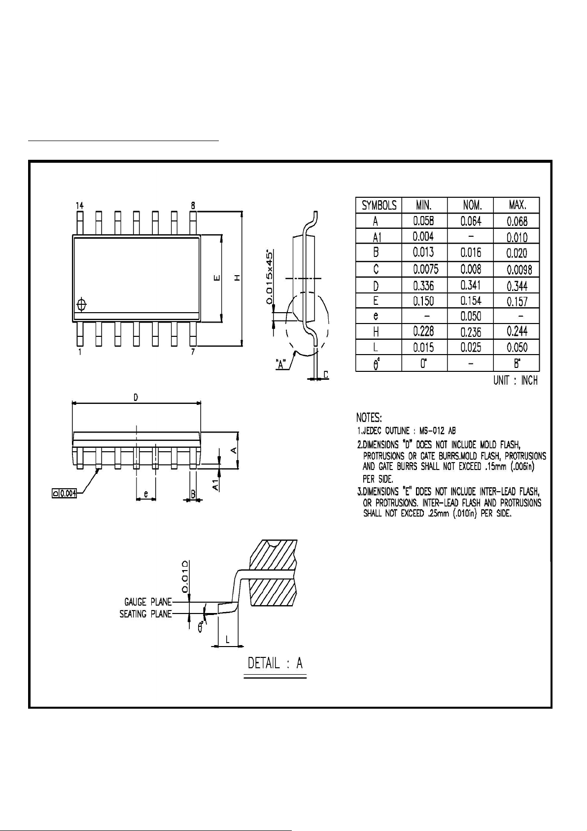
14-Lead SOIC Package
APPLICATIONS:
Graphic Cards
DDR memory power supply
Data communication
5V to 3.xV DC-to-DC
PIN CONFIGURATION:
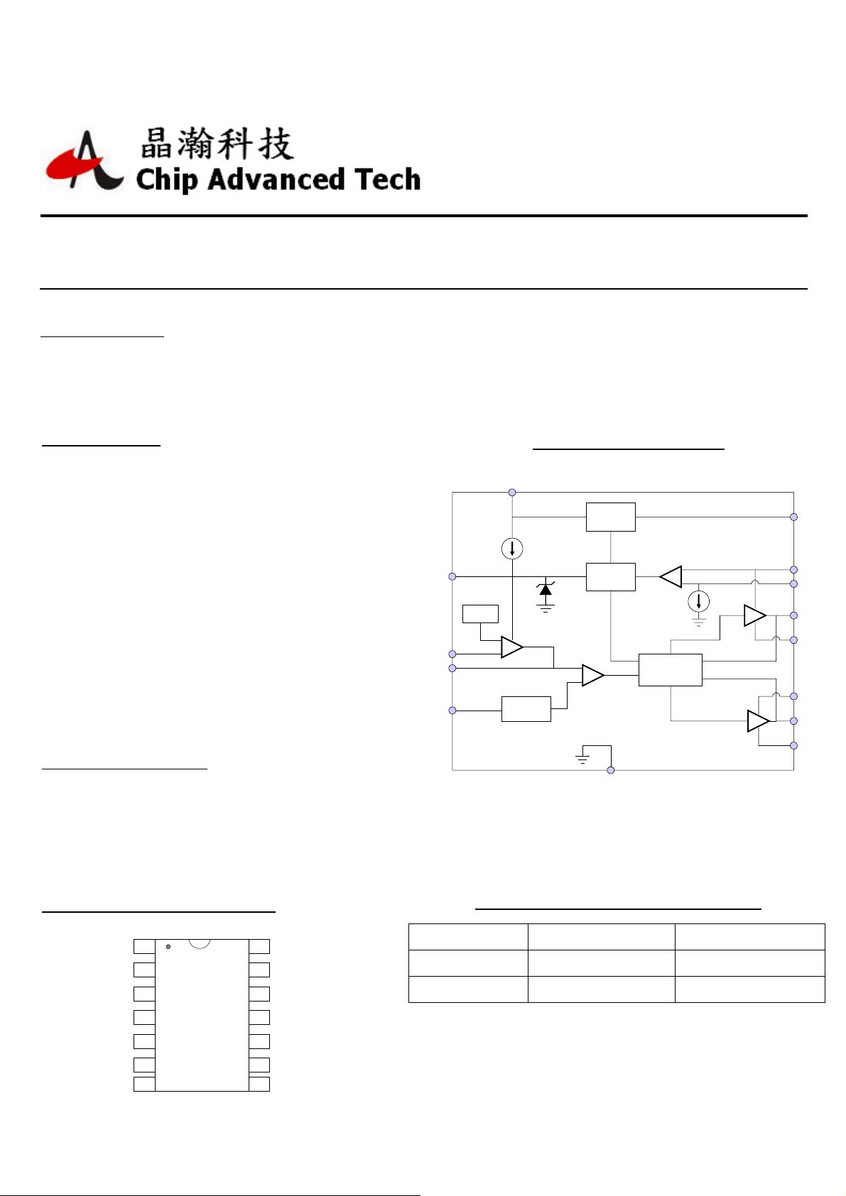
BLOCK DIAGRAM
VCC
Power On
Reset
SS
Vref
0.8V
FB
COMP
RT
Oscillator
ORDERING INFORMATION:
Soft-Start
Gate Control
GND
EN
PHASE
OCSET
UGATE
BOOT
PVCC
LGATE
PGND
OCSET
COMP
CAT7522
GND
RT
SS
FB
EN
1
2
3
4
5
6
7
(Top View)
14
13
12
11
10
9
8
VCC
PVCC
LGATE
PGND
BOOT
UGATE
PHASE
Part Number Package Operating Temp(℃)
CAT7522 14L SOIC (Normal) 0-70
CAT7522G 14L SOIC (Pb free) 0-70
Page 2
CAT7522
SPECIFICATIONS
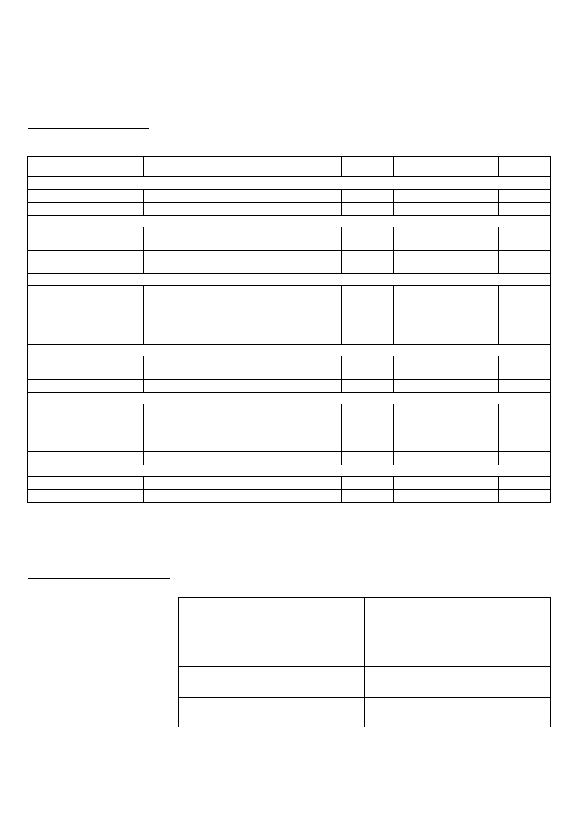
Electrical Specifications
Parameter
VCC Supply Current
Nominal Supply
Shutdown Supply
Recommended Operating Conditions, Unless Otherwise Noted
Symbol Test Conditions Min Typ. Max Unit
ICC EN=Vcc;UGATE & LGATE open 5 mA
EN=0 V 50
100
μA
Power On Reset
Rising Vcc Threshold V
Falling Vcc Threshold V
Enable-Input Threshold V
Rising V
Threshold 1.27 V
OCSET
=4.5V 10.4 V
OCSET
=4.5V 8.8 V
OCSET
=4.5V 0.8 2.0 V
OCSET
Oscillator
Free running frequency RT=open ;Vcc=12 V 170 220 260 kHz
Ramp Amplitude
Reference Voltage
ΔV
V
OSC
-1 +1 %
REF
RT=open 1.9 Vp-p
Tolerance
Reference Voltage 0.8 V
ERROR Amplifier
DC Gain 90 dB
Gain-Bandwidth Product GBW 15 MHz
Slew Rate SR COMP=10pF 6
V/μs
Gate Driver
Upper Gate Source I
V
UGATE
BOOT-VPHASE
=12V;V
UGATE
=6V
450 mA
(Note 1)
Upper Gate Sink R
Lower Gate Source I
Lower Gate Sink R
I
UGATE
Vcc=12V;V
LGATE
I
LGATE
=0.3A (Note 1) 5.5 10
LGATE
=6V (Note 1) 690 mA
LGATE
=0.3A (Note 1) 3.5 6.5
LGATE
Ω
Ω
Protection
OCSET Current Source I
Soft S tart Current ISS 10
Note:
1. Guaranteed by design; not production tested
V
OCSET
.
OCSET
=4.5V 170 200 230
μA
μA
ABSOLUTE RATING
Parameter Max. Rating
Vcc, Supply Voltage 15V
Boot Voltage(V
BOOT-VPHASE
) 15V
Input & Output Voltage Vcc + 0.3V
GND - 0.3V
Operating Temperature
Storage Temperature
Max. Junction Temperature
0℃ to 70℃
-65℃ to 150℃
150℃
ESD Classification Class 2
Page 3

CAT7522
TYPICAL APPLICATION
R4
12V
C6
R8
R9
R10
Vout=0.8x(1+R10/R9)
Vout
C10
C11
C12
12V
D1
C4
R6
R5
U2
45
45
678
123
C7
R7
L1
1 2
123
C3
C2
R3
C1
R1
U1
1
RT
RT
OC
2
OCSET
SS
3
SS
COMP
4
COMP
FB
5
FB
EN
6
EN
7 8
GND PHASE
C5
VCC
PVCC
LGATE
PGND
BOOT
UGATE
14
13
12
11
10
9
LG
UG
PHASE
R2 3K
U3
678
C8
L2
1 2
C9
12V
[Note]:
1. C1~C5 & C6~C10 are flexible in using considering cost and system performance, the above 5 devices and
6 devices are designed for internal characteristics testing use.
2. The recommended applications shall be customer design-in orientation to fit each customers demand. Based
on the nature of customers demand-oriented, please contact CAT or agent for design support service.
Page 4

CAT7522
PIN DESCRIPTION
RT
This pin allows oscillator switching frequency to be
adjusted by the resistor value (R
GND. The nominal 220 kHz switching frequency is
increased according to the following equation:
Fs (kHz) ~= 106 / Rt + 220 kHz
The following table lists some resistors for Rt in
common use and their approximately corresponding
switching frequency:
Fs(K Hz) 220 300 400 500 600 700 800 900 1000
Rt (K ohm) NC 22 6.8 4.1 2.9 2.2 1.7 1.5 1.28
OCSET
A r e s i ste r , R
MOSFET (On resistance r
source I
OCS
, from this pin to the drain of upper
OCSET
DS(ON)
to determine the converter over-current
(OC) trip point by the following equation,
I
PEAK
= I
OCS
* R
OCSET/rDS(ON)
Over-current (OC) trip cycles the soft-start function.
SS
Connect a capacitor from this pin to GND, and the
capacitor along with and internal 10μ A current
source sets the soft start interval of the converter.
COMP and FB
COMP is the error amplifier output. FB is the interval
input of error amplifier. These 2 pins are used to
compensate the voltage-control feedback loop of the
converter.
EN
EN means open-collector enable pin, pulling under
1V to disable the converter. In shut-down mode, the
soft-start pin is discharged and the UGATE and
LGATE pins are held low.
UGATE
Connect UGATE to the upper MOSFET gate. This
pin provides the gate drive for upper MOSFET. It is
), from this pin to
t
), and internal current
also monitored by the adaptive shoot through
protection function to determine when upper
MOSFET has turned off.
LGATE
Connect UGATE to the lower MOSFET gate. This
pin provides the gate drive for lower MOSFET. It is
also monitored by the adaptive shoot through
protection function to determine when lower
MOSFET has turned off.
PHASE
This pin is used to monitor the voltage drop across
the MOSFET for over-current protection. This pin
also provides the return path for the upper gate drive.
BOOT
This pin provides bias voltage to the upper MOSFET
driver. A bootstrap circuit may used to generate
BOOT voltage suitable to drive a standard N-channel
MOSFET.
VCC
Provide 12V bias supply for the chip.
GND
Signal ground of the chip
PVCC
Supply voltage for lower gate drive
PGND
Power ground pin, connected to lower MOSFET
source to this pin.
Page 5
FUNCTION DESCRIPTION
OUTPUT REGULATION
The output voltage level setting is
VOUT = 0.8V * (1 + R10 / R9)
Please reference the application diagram.
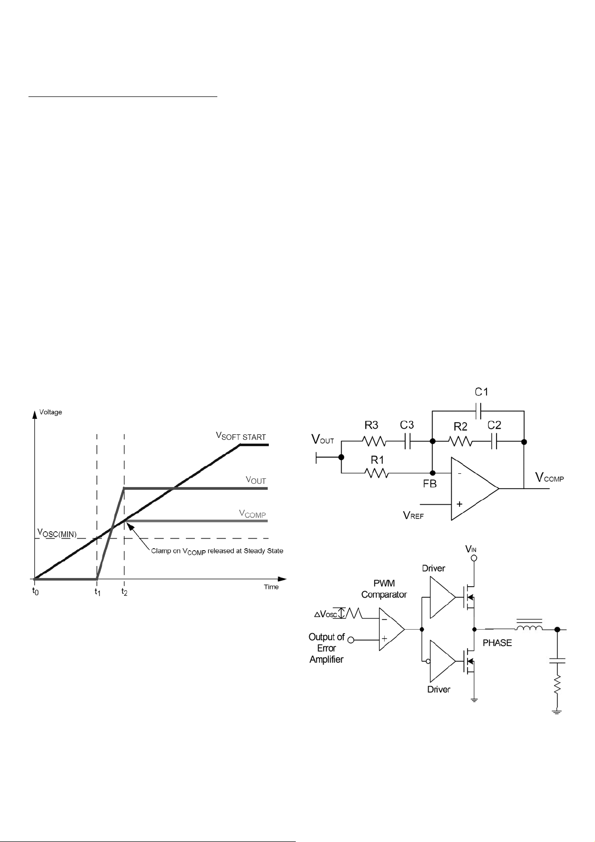
SOFT-START
In CAT7522, an internal 10uA current source charges
an external capacitor (Css) on the SS pin to 4V.
Soft-start clamps the error amplifier output (COMP
pin) to the SS pin voltage. Figure 1 shows the
soft-start interval. The formula to calculate the interval
is:
t1 = Css / Iss *Vosc (min)
t
where: Css : Soft start capacitor.
Iss : 10uA, soft start current.
Vosc(min) = 1.35V, bottom of oscillator.
= t2 – t1 = Css / Iss * Vout / Vin * △Vosc
soft_start
△
Vosc = 1.9V, peak to peak oscillator amplitude.
to VIN) exceeds the voltage across R
overcurrent function initiates a soft-start sequence.
The peak inductor current (I
following equation:
I
= 200uA * R
peak
ocset
/ r
) is determined by the
peak
DS(on)
OCSET
, the
A small ceramic capacitor should be placed in parallel
with R
to smooth the voltage across R
OCSET
OCSET
in the
presence of switching noise on the input voltage.
FEEDBACK COMPENSATION
The compensation required for VOUT1 and VOUT2
is similar to many other switching regulators.
The figure 2 shows type-3 compensation, but the
simpler type 2 is also possible, under the right
conditions. A simple rule of thumb of type-3
compensation is that when buck capacitors are used
on the outputs, the effective ESR is about smaller
than 3 mohm. Notes that the component labels match
the equations given in this section, but may not match
other diagrams in this datasheet.
Figure 1
OVERCURRENT PROTECTION
The overcurrent function protects the converter from
a shorted output by using the upper MOSs
on-resistance, r
to monitor the current.
DS(ON)
The overcurrent function cycles the soft-start
function in a hiccup mode to provide fault protection.
A resistor (R
) programs the overcurrent trip level.
OCSET
An internal 200uA (typ i c a l ) c u r r e n t s i n k d e v e l o p s a
voltage across R
that is reference to Vin. When the
OCSET
voltage across the upper MOSFET (also referenced
Figure 2
Figure 3
In Figure 2 and 3, the output voltage (Vout) is
regulated to the Reference voltage level. The error
amplifier output (V
COMP
) is compared with the
oscillator (OSC) triangular wave to provide a
Lo
V out
C
ESR
Page 6
pulse-width modulated (PWM) wave with an
amplitude of VIN at the PHASE node. The PWM
wave is smoothed by the output filter (LO and CO).
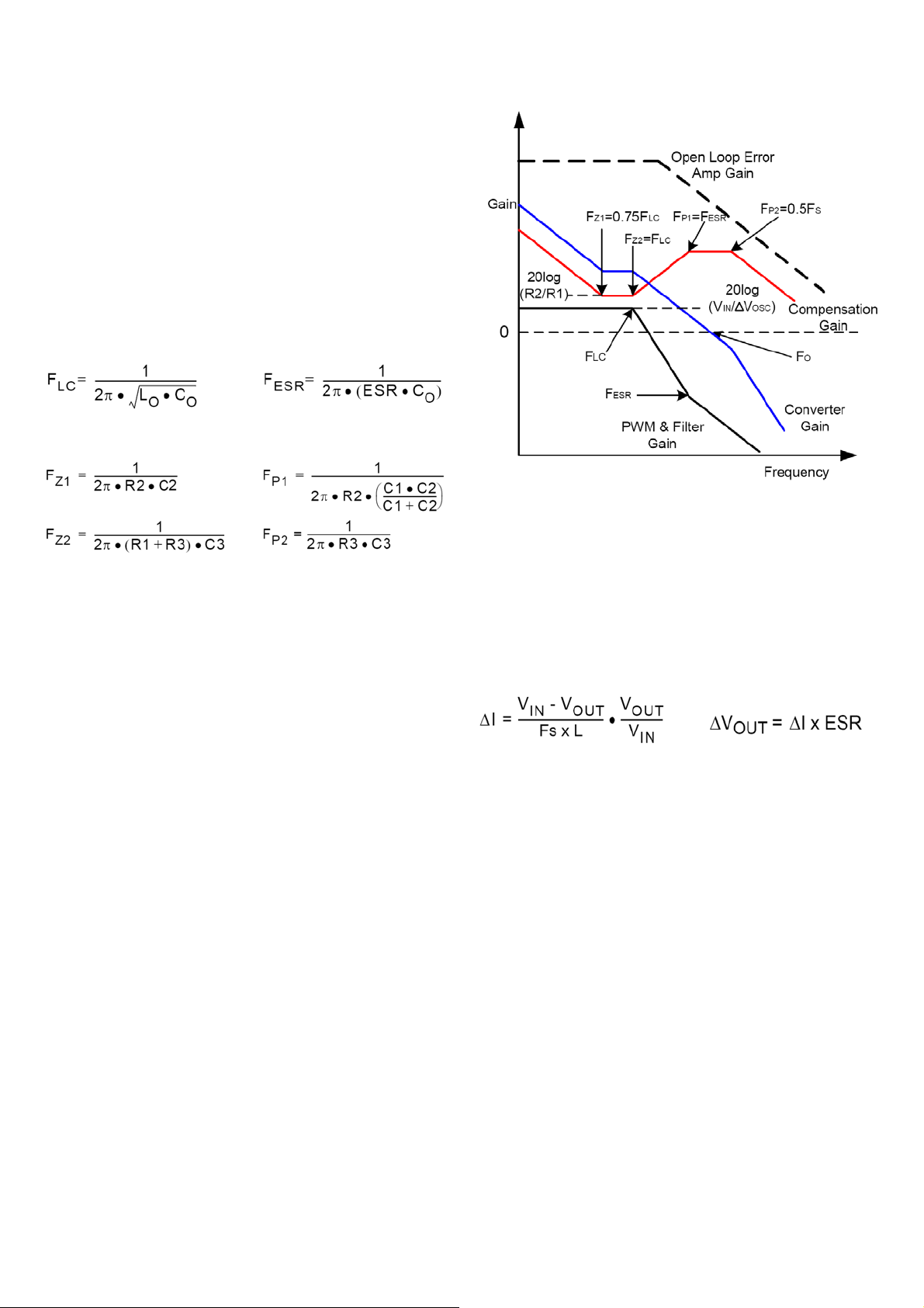
The closed loop transfer function of the converter
includes two part, the error amplifier compensation and
the modulator transfer functions. The modulator transfer
function is dominated by a DC gain and the output filter,
with a double pole break frequency at FLC and a zero at
F
. The DC Gain of the modulator is simp ly the input
ESR
voltag e (V I N ) d i vi d ed b y th e peak-to-peak oscillator
voltage △V
OSC
.
The poles and zeros location of the type-3 compensation
of error amplifier list below.
The goal of the compensation network is to provide a
closed loop transfer function with the highest 0dB
crossing frequency (fco) and adequate phase margin.
The following guidelines will help users to design the
compensation network.
(1). Select the desired zero crossover frequency FCO.
FCO is usually 1/4 ~ 1/10 switch frequency (FS).
(2). Choose a value for R1.
(3). Pick gain R2/R1 for desired F
R2 can be calculated by
Vin /△V
(4). Place F
(5). Place FP1 at F
* FLC/F
OSC
about 0.75 * FLC to calculate the C2.
Z1
ESR
* R2/R1 = 1
CO
to calculate the C1.
. To simplify, the
CO
(6). Place FZ2 about FLC.
(7). Place F
Combined (6), (7) the R3 and C3 will be calculated.
about 0.5 * Fs.
P2
(8). Estimate the stability, Modify FCO and R2/R1
gain then repeat if necessary.
The Figure 4 shows an asymptotic plot of the
converter’s gain vs. frequency.
Figure 4
OUTPUT INDUCTOR SELECTION
The output inductor is selected to meet the output
voltage ripple requirements and affects the load
transient response. Higher inductance reduces the
inductor's ripple current and induces lower output
ripple voltage. The ripple voltage and current are
approximated by the following equations:
Although increase the inductance reduce the ripple
current and voltage, but the large inductance reduces
the regulator’s response time to load transient.
Increasing the switching frequency (Fs) for a given
inductor also reduces the ripple current and voltage
but it will increase the switching loss of the power
MOS.
To select the inductor value, a guideline is to choose
the ripple current (△I) to be approximately
10%~50% of the maximum output cur r e nt. Once the
inductor value has been chosen, select an inductor that
is capable of carrying the required peak current
without going into saturation. It is also important to
have the inductance tolerance specified to keep the
accuracy of the system controlled. Using 20% for the
inductance (at room temperature) are reasonable
tolerances that most manufacturers can meet. In some
types of inductors, especially core that is made of
ferrite, the ripple current will increase abruptly when it
saturates. This will result in a larger output ripple
voltage.
Page 7

OUTPUT CAPACITORS SELECTION
An output capacitor is required to filter the output and
supply the load transient current. Higher Capacitor
value and lower ESR reduce the output ripple and the
load transient drop. These requirements are met with a
mix of capacitors and careful layout.
In typical switching regulator design, the ESR of the
output capacitor bank dominates the transient response.
The number of output capacitors can be determined by
using the following equations:
△
V
= change in output voltage due to ESR
ESR
(assigned by the designer).
△
I
= load transient.
OUT
ESR
= maximum ESR per capacitor (specified
CAP
in manufacturer’s data sheet).
ESR
= maximum allowable ESR.
MAX
High frequency decoupling capacitors should be
placed as close to the power pins of the load as
physically possible. Consult the capacitors
manufacturer to make sure the decoupling
requirements.
POWR MOS SELECTION
CAT7522 requires 2 N-channel power MOSs for
each PWM output. These should be selected base on
, gate supply voltage, gate charge (capacitance)
R
ds(on)
and thermal management requirements. In general,
the upper power MOS should be chosen to minimize
the gate charge, since switching loses dominate.
Since the lower power MOS is on most of the time,
low R
should be the main consideration.
ds(on)
It can be advantageous to use multiple power MOSs
to reduce power consumption. By placing a number
of MOSs in parallel, the effective R
ds(on)
is reduced,
thus reducing the ohmic power loss. However,
placing MOSs in parallel increases the gate
capacitance so that switching losses increase. As long
as adding another parallel MOS reduces the ohmic
power loss more than the switching losses increase,
there is some advantage to doing so.
The following equations can be used to calculate
power dissipation in the power MOSs.
Where,
D is the duty cycle = Vout / Vin.
tSW is the switching interval.
Fs is the switching frequency.
CONTACT:
HEADQUARTERS:
8F, No.1, Jin-Shan 7
300 Taiwan, ROC.
Tel: +886-3-666-8301
Fax: +886-3-666-8630
Website: http://www.chipadvanced.com
th
St., Hsin-Chu,
Page 8
CAT7522
MECHINICAL DIMENSION
 Loading...