

Datasheet CAT22C10JA-20TE13, CAT22C10J-30TE13, CAT22C10J-20TE13, CAT22C10PI-30TE13, CAT22C10PI-20TE13 Datasheet (CTLST)
...Page 1
CAT22C10
256-Bit Nonvolatile CMOS Static RAM
FEATURES
■ Single 5V Supply
■ Fast RAM Access Times:
–200ns
–300ns
■ Infinite E
■ CMOS and TTL Compatible I/O
■ Power Up/Down Protection
■ 100,000 Program/Erase Cycles (E
2
PROM to RAM Recall
2
PROM)
DESCRIPTION
The CAT22C10 NVRAM is a 256-bit nonvolatile memory
organized as 64 words x 4 bits. The high speed Static
RAM array is bit for bit backed up by a nonvolatile
E2PROM array which allows for easy transfer of data
from RAM array to E2PROM (STORE) and from
E2PROM to RAM (RECALL). STORE operations are
completed in 10ms max. and RECALL operations typically within 1.5µs. The CAT22C10 features unlimited
RAM write operations either through external RAM
■ Low CMOS Power Consumption:
–Active: 40mA Max.
–Standby: 30 µA Max.
■ JEDEC Standard Pinouts:
–18-pin DIP
–16-pin SOIC
■ 10 Year Data Retention
■ Commercial, Industrial and Automotive
Temperature Ranges
writes or internal recalls from E2PROM. Internal false
store protection circuitry prohibits STORE operations
when VCC is less than 3.0V.
The CAT22C10 is manufactured using Catalyst’s advanced CMOS floating gate technology. It is designed
to endure 100,000 program/erase cycles (E2PROM)
and has a data retention of 10 years. The device is
available in JEDEC approved 18-pin plastic DIP and 16pin SOIC packages.
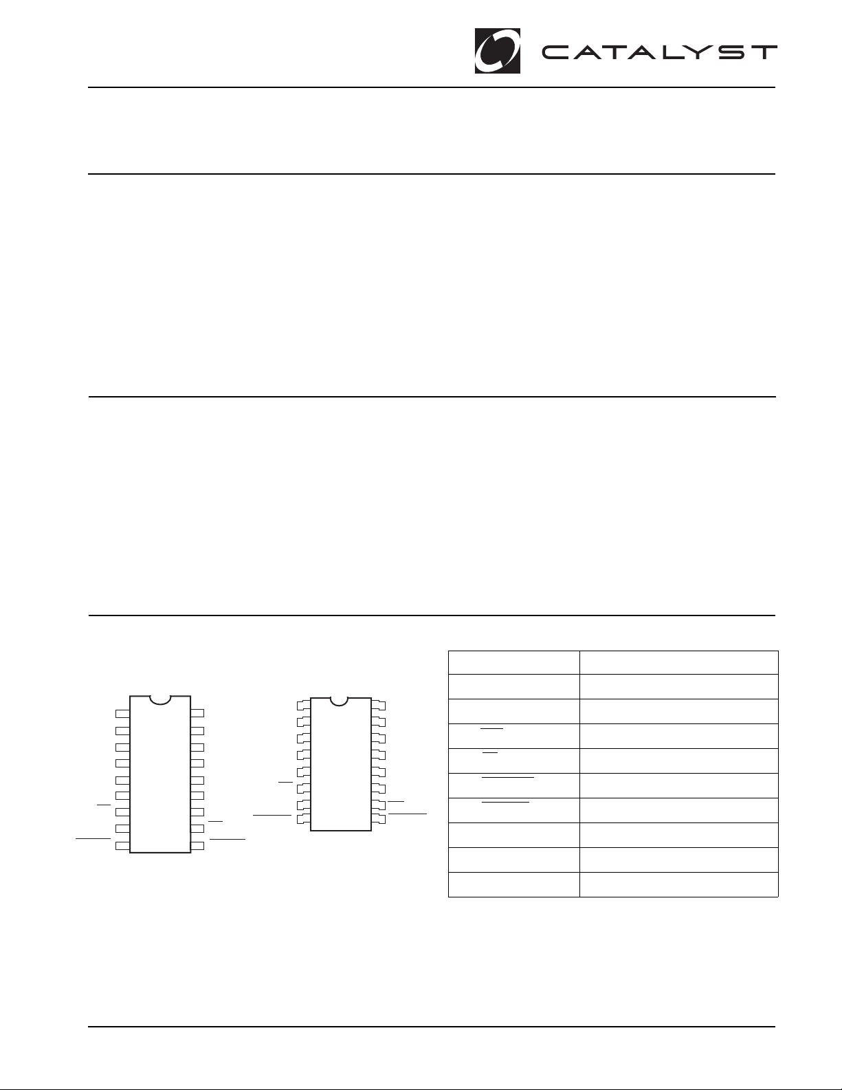
PIN CONFIGURATION
V
NC
A
4
A
3
A
2
A
1
A
0
CS
V
ss
STORE
© 1998 by Catalyst Semiconductor, Inc.
Characteristics subject to change without notice
18
1
2
17
3
16
4
15
5
14
6
13
7
12
8
9
10
cc
NC
A
5
I/O
I/O
I/O
I/O
WE
11
RECALL
22C10 F01 22C10 F02
SOIC Package (J)DIP Package (P)
A
1
4
A
3
A
2
A
3
2
1
0
1
A
0
CS
V
ss
STORE RECALL
16
15
2
14
3
4
5
6
7
8
13
12
11
10
PIN FUNCTIONS
Pin Name Function
A0–A
5
V
cc
A
5
I/O
4
I/O
3
I/O
2
I/O
1
WE
9
I/O0–I/O
3
WE Write Enable
CS Chip Select
RECALL Recall
STORE Store
V
CC
V
SS
NC No Connect
1
Address
Data In/Out
+5V
Ground
Doc. No. 25018-0A 2/98 N-1
Page 2
CAT22C10
BLOCK DIAGRAM
2
E
PROM ARRAY
ROW
SELECT
COLUMN SELECT
CONTROL
LOGIC
CS WE
STATIC RAM
ARRAY
READ/WRITE
CIRCUITS
I/O0I/O1I/O2I/O
STORE
RECALL
3
MODE SELECTION
(1)(2)(3)
A
A
A
A
A
A
STORE
RECALL
0
1
2
3
4
5
Input
Mode
CSCS
CS
CSCS
WEWE
WE
WEWE
RECALLRECALL
RECALL
RECALLRECALL
STORESTORE
STORE I/O
STORESTORE
Standby H X H H Output High-Z
RAM Read L H H H Output Data
RAM Write L L H H Input Data
(E2PROM→RAM) X H L H Output High-Z RECALL
5153 FHD F02
(E2PROM→RAM) H X L H Output High-Z RECALL
(RAM→E2PROM) X H H L Output High-Z STORE
(RAM→E2PROM) H X H L Output High-Z STORE
POWER-UP TIMING
(4)
Symbol Parameter Min. Max. Units
VCCSR VCC Slew Rate 0.5 0.005 V/ms
Note:
(1) RECALL signal has priority over STORE signal when both are applied at the same time.
(2) STORE is inhibited when RECALL is active.
(3) The store operation is inhibited when VCC is below ≈ 3.0V.
(4) This parameter is tested initially and after a design or process change that affects the parameter.
Doc. No. 25018-0A 2/98 N-1
2
Page 3
CAT22C10
ABSOLUTE MAXIMUM RATINGS*
Temperature Under Bias ................. –55°C to +125°C
Storage Temperature....................... –65°C to +150°C
Voltage on Any Pin with
Respect to Ground
VCC with Respect to Ground ................ -2.0V to +7.0V
Package Power Dissipation
Capability (Ta = 25°C)................................... 1.0W
(2)
..............-2.0 to +VCC +2.0V
*COMMENT
Stresses above those listed under “Absolute Maximum
Ratings” may cause permanent damage to the device.
These are stress ratings only, and functional operation
of the device at these or any other conditions outside of
those listed in the operational sections of this specification is not implied. Exposure to any absolute maximum
rating for extended periods may affect device performance and reliability.
Lead Soldering Temperature (10 secs) ............ 300°C
Output Short Circuit Current
(3)
........................ 100 mA
RELIABILITY CHARACTERISTICS
Symbol Parameter Min. Max. Units Reference Test Method
(1)
N
T
V
I
END
DR
ZAP
LTH
(1)
(1)
(1)(4)
Endurance 100,000 Cycles/Byte MIL-STD-883, Test Method 1033
Data Retention 10 Years MIL-STD-883, Test Method 1008
ESD Susceptibility 2000 Volts MIL-STD-883, Test Method 3015
Latch-Up 100 mA JEDEC Standard 17
D.C. OPERATING CHARACTERISTICS
VCC = +5V ±10%, unless otherwise specified.
Limits
Symbol Parameter Min. Typ. Max. Unit Conditions
I
CC
Current Consumption 40 mA All Inputs = 5.5V
(Operating) TA = 0°C
All I/O’s Open
I
SB
Current Consumption 30 µA CS = V
CC
(Standby) All I/O’s Open
I
LI
I
LO
V
IH
V
IL
V
OH
V
OL
V
DH
Input Current 10 µA0 ≤ VIN ≤ 5.5V
Output Leakage Current 10 µA0 ≤ V
High Level Input Voltage 2 V
CC
V
OUT
≤ 5.5V
Low Level Input Voltage 0 0.8 V
High Level Output Voltage 2.4 V IOH = –2mA
Low Level Output Voltage 0.4 V IOL = 4.2mA
RAM Data Holding Voltage 1.5 5.5 V V
CC
CAPACITANCE TA = 25°C, f = 1.0 MHz, VCC = 5V
Symbol Parameter Max. Unit Conditions
(1)
C
I/O
(1)
C
IN
Note:
(1) This parameter is tested initially and after a design or process change that affects the parameter.
(2) The minimum DC input voltage is -0.5V. During transitions, inputs may undershoot to -2.0V for periods of less than 20 ns. Maximum DC
voltage on output pins is VCC +0.5V, which may overshoot to VCC +2.0V for periods of less than 20 ns.
(3) Output shorted for no more than one second. No more than one output shorted at a time.
(4) Latch-up protection is provided for stresses up to 100 mA on address and data pins from -1V to VCC +1V.
Input/Output Capacitance 10 pF V
Input Capacitance 6 pF V
I/O
IN
= 0V
= 0V
3
Doc. No. 25018-0A 2/98 N-1
Page 4

CAT22C10
A.C. CHARACTERISTICS, Write Cycle
VCC = +5V ±10%, unless otherwise specified.
22C10-20 22C10-30
Symbol Parameter Min. Max. Min. Max. Unit Conditions
t
t
t
t
t
t
t
t
WZ
t
WC
CW
AS
WP
WR
DW
DH
(1)
OW
Write Cycle Time 200 300 ns
CS Write Pulse Width 150 150 ns
Address Setup Time 50 50 ns CL = 100pF
Write Pulse Width 150 150 ns +1TTL gate
Write Recovery Time 25 25 ns VOH = 2.2V
Data Valid Time 100 100 ns VOL = 0.65V
Data Hold Time 0 0 ns VIH = 2.2V
Output Disable Time 100 100 ns VIL = 0.65V
Output Enable Time 0 0 ns
A.C. CHARACTERISTICS, Read Cycle
VCC = +5V ±10%, unless otherwise specified.
22C10-20 22C10-30
Symbol Parameter Min. Max. Min. Max. Unit Conditions
t
RC
t
AA
t
CO
t
OH
(1)
t
LZ
(1)
t
HZ
Note:
(1) This parameter is tested initially and after a design or process change that affects the parameter.
Read Cycle Time 200 300 ns CL = 100pF
Address Access Time 200 300 ns +1TTL gate
CS Access Time 200 300 ns VOH = 2.2V
Output Data Hold Time 0 0 ns VOL = 0.65V
CS Enable Time 0 0 ns VIH = 2.2V
CS Disable Time 100 100 ns V
= 0.65V
IL
Doc. No. 25018-0A 2/98 N-1
4
Page 5

A.C. CHARACTERISTICS, Store Cycle
VCC = +5V ±10%, unless otherwise specified.
Limits
Symbol Parameter Min. Max. Units Conditions
t
STZ
t
OST
t
STC
t
STP
(1)
(1)
Store Time 10 ms
Store Pulse Width 200 ns CL = 100pF + 1TTL gate
Store Disable Time 100 ns VOH = 2.2V, VOL = 0.65V
Store Enable Time 0 ns VIH = 2.2V, VIL = 0.65V
A.C. CHARACTERISTICS, Recall Cycle
VCC = +5V ±10%, unless otherwise specified.
Limits
Symbol Parameter Min. Max. Units Conditions
t
RCC
Recall Cycle Time 1.4 µs
CAT22C10
t
RCP
t
RCZ
t
ORC
t
ARC
Note:
(1) This parameter is tested initially and after a design or process change that affects the parameter.
Recall Pulse Width 300 ns CL = 100pF + 1TTL gate
Recall Disable Time 100 ns VOH = 2.2V, VOL = 0.65V
Recall Enable Time 0 ns VIH = 2.2V, VIL = 0.65V
Recall Data Access Time 1.1 µs
5
Doc. No. 25018-0A 2/98 N-1
Page 6

CAT22C10
DEVICE OPERATION
The configuration of the CAT22C10 allows a common
address bus to be directly connected to the address
inputs. Additionally, the Input/Output (I/O) pins can be
directly connected to a common I/O bus if the bus has
less than 1 TTL load and 100pF capacitance. If not, the
I/O path should be buffered.
When the chip select (CS) pin goes low, the device is
activated. When CS is forced high, the device goes into
the standby mode and consumes very little current. With
the nonvolatile functions inhibited, the device operates
like a Static RAM. The Write Enable (WE) pin selects a
write operation when WE is low and a read operation
when WE is high. In either of these modes, an array byte
(4 bits) can be addressed uniquely by using the address
lines (A0–A5), and that byte will be read or written to
through the Input/Output pins (I/O0–I/O3).
The nonvolatile functions are inhibited by holding the
STORE input and the RECALL input high. When the
RECALL input is taken low, it initiates a recall operation
which transfers the contents of the entire E2PROM array
into the Static RAM. When the STORE input is taken low,
it initiates a store operation which transfers the entire
Static RAM array contents into the E2PROM array.
Standby Mode
The chip select (CS) input controls all of the functions of
the CAT22C10. When a high level is supplied to the CS
pin, the device goes into the standby mode where the
outputs are put into a high impendance state and the
power consumption is drastically reduced. With ISB less
than 100µA in standby mode, the designer has the
flexibility to use this part in battery operated systems.
Read
When the chip is enabled (CS = low), the nonvolatile
functions are inhibited (STORE = high and RECALL =
high). With the Write Enable (WE) pin held high, the data
in the Static RAM array may be accessed by selecting an
address with input pins A0–A5. This will occur when the
outputs are connected to a bus which is loaded by no
more than 100pF and 1 TTL gate. If the loading is greater
than this, some additional buffering circuitry is recommended.
Figure 1. Read Cycle Timing
ADDRESS
CS
DATA I/O
t
AA
t
RC
t
CO
t
LZ
DATA VALID
t
OH
t
HZ
HIGH-Z
5153 FHD F06
Doc. No. 25018-0A 2/98 N-1
6
Page 7

Write
With the chip enabled and the nonvolatile functions
inhibited, the Write Enable (WE) pin will select the write
mode when driven to a low level. In this mode, the
address must be supplied for the byte being written.
After the set-up time (tAS), the input data must be
supplied to pins I/O0–I/O3. When these conditions, in-
Figure 2. Write Cycle Timing
ADDRESS
CS
t
AS
WE
CAT22C10
cluding the write pulse width time (tWP) are met, the data
will be written to the specified location in the Static RAM.
A write function may also be initiated from the standby
mode by driving WE low, inhibiting the nonvolatile functions, supplying valid addresses, and then taking CS low
and supplying input data.
t
WC
t
CW
t
WP
t
WR
DATA IN
DATA OUT
Figure 3. Early Write Cycle Timing
ADDRESS
CS
WE
t
DW
DATA VALID
t
WZ
HIGH-Z
t
WC
t
CW
t
AS
t
WP
t
DW
t
t
DH
DH
t
t
WR
OW
5153 FHD F04
DATA IN
DATA OUT
7
DATA VALID
HIGH-Z
5153 FHD F05
Doc. No. 25018-0A 2/98 N-1
Page 8

CAT22C10
Recall
At anytime, except during a store operation, taking the
RECALL pin low will initiate a recall operation. This is
independent of the state of CS, WE, or A0–A5. After the
RECALL pin has been held low for the duration of the
Recall Pulse Width (t
), the recall will continue inde-
RCP
pendent of any other inputs. During the recall, the entire
contents of the E2PROM array is transferred to the Static
RAM array. The first byte of data may be externally
accessed after the recalled data access time from end of
recall (t
) is met. After this, any other byte may be
ARC
accessed by using the normal read mode.
If the RECALL pin is held low for the entire Recall Cycle
time (t
), the contents of the Static RAM may be
RCC
immediately accessed by using the normal read mode.
A recall operation can be performed an unlimited number of times without affecting the integrity of the data.
The outputs I/O0–I/O3 will go into the high impedance
state as long as the RECALL signal is held low.
Store
At any time, except during a recall operation, taking the
STORE pin low will initiate a store operation. This takes
place independent of the state of CS, WE or A0–A5. The
STORE pin must be held low for the duration of the Store
Pulse Width (t
) to ensure that a store operation is
STP
initiated. Once initiated, the STORE pin becomes a
“Don’t Care”, and the store operation will complete its
transfer of the entire contents of the Static RAM array
into the E2PROM array within the Store Cycle time
(t
). If a store operation is initiated during a write cycle,
STC
the contents of the addressed Static RAM byte and its
corresponding byte in the E2PROM array will be unknown.
During the store operation, the outputs are in a high
impedance state. A minimum of 100,000 store operations can be performed reliably and the data written into
the E2PROM array has a minimum data retention time
of 10 years.
DATA PROTECTION DURING POWER-UP AND
POWER-DOWN
The CAT22C10 has on-chip circuitry which will prevent
a store operation from occurring when VCC falls below
3.0V typ. This function eliminates the potential hazard of
spurious signals initiating a store operation when the
system power is below 3.0V typ.
Figure 4. Recall Cycle Timing
ADDRESS
RECALL
CS
DATA I/O
t
RCZ
Figure 5. Store Cycle Timing
STORE
DATA I/O
t
STZ
t
STP
t
RCP
HIGH-Z
t
STC
HIGH-Z
t
RCC
t
ARC
t
ORC
DATA UNDEFINED DATA VALID
t
OST
5153 FHD F08
Doc. No. 25018-0A 2/98 N-1
5153 FHD F07
8
Page 9

ORDERING INFORMATION
Prefix Device # Suffix
CAT22C10
CAT
Optional
Company ID
22C10 J I -TE13
Product
Number
Temperature Range
Blank = Commercial (0˚ - 70˚C)
-20
Tape & Reel
TE13: 2000/Reel
I = Industrial (-40˚ - 85˚C)
A = Automotive (-40˚ - 105˚C)*
Package
P: PDIP
J: SOIC (JEDEC)
Speed
20: 200ns
30: 300ns
* -40˚ to +125˚C is available upon request
Notes:
(1) The device used in the above example is a 22C10JI-20TE13 (SOIC, Industrial Temperature, 200ns Access Time, Tape & Reel)
22C10 F08
9
Doc. No. 25018-0A 2/98 N-1
Page 10

CAT22C10
Doc. No. 25018-0A 2/98 N-1
10
 Loading...