

Page 1

6-Channel Capacitive Touch Sensor with
SMBus
Protocol
VDD
GND
Capacitive Touch Sensing
Algorithm
CS1 CS2 CS4 CS5
SMCLK
SMDATA
ALERT#
CS6
CS3 /
SG
Proximity Detection & Signal Guard
CAP1296
PRODUCT FEATURES
General Description
The CAP1296 which incorporates RightTouch® technology,
is a multiple channel capacitive touch sensor. It contains six
(6) individual capacitive touch sensor inputs with
programmable sensitivity for use in touch sensor
applications. Each sensor input is calibrated to compensate
for system parasitic capacitance and automatically
recalibrated to compensate for gradual environmental
changes.
In addition, the CAP1296 can be configured to detect
proximity on one or more channels with an optional signal
guard to reduce noise sensitivity and to isolate the proximity
antenna from nearby conductive surfaces that would
otherwise attenuate the e-field.
The CAP1296 includes Multiple Pattern Touch recognition
that allows the user to select a specific set of buttons to be
touched simultaneously. If this pattern is detected, a status
bit is set and an interrupt is generated.
The CAP1296 has Active and Standby states, each with its
own sensor input configuration controls. The Combo state
allows a combination of sensor input controls to be used
which enables one or more sensor inputs to operate as
buttons while another sensor input is operating as a
proximity detector. Power consumption in the Standby and
Combo states is dependent on the number of sensor inputs
enabled as well as averaging, sampling time, and cycle
time. Deep Sleep is the lowest power state available,
drawing 5µA (typical) of current. In this state, no sensor
inputs are active, and communications will wake the device.
Datasheet
Applications
Desktop and Notebook PCs
LCD Monitors
Consumer Electronics
Appliances
Features
Six (6) Capacitive Touch Sensor Inputs
— Programmable sensitivity
— Automatic recalibration
— Calibrates for parasitic capacitance
— Individual thresholds for each button
Proximity Detection
Signal Guard
— Isolates the proximity antenna from attenuation
— Reduces system noise sensitivity effects on inputs
Mu ltiple Button Pattern Detection
Power Button Support
Press and Hold Feature for Volume-like Applications
3.3V or 5V Supply
Analog Filtering for System Noise Sources
RF Detection and Avoidance Filters
Digital EMI Blocker
8kV ESD Rating on All Pins (HBM)
Low Power Operation
— 5µA quiescent current in Deep Sleep
— 50µA quiescent current in Standby (1 sensor input
monitored)
— Samples one or more channels in Standby
SMBus / I
Available in a 10-pin 3mm x 3mm DFN RoHS compliant
package
2
C Compliant Communication Interface
Block Diagram
2013 Microchip Technology Inc. DS01569A-page 1
Page 2

6-Channel Capacitive Touch Sensor with Proximity Detection & Signal Guard
Ordering Information:
ORDERING
NUMBER PACKAGE FEATURES
Datasheet
CAP1296-1-AIA-TR 10-pin DFN 3mm x 3mm
(RoHS compliant)
Reel size is 4,000 pieces for 10-pin DFN
This product meets the halogen maximum concentration values per IEC 61249-2-21
Six capacitive touch sensor inputs, SMBus interface,
SMBus address 0101_000(r/w). Proximity and signal
guard.
DS01569A-page 2 2013 Microchip Technology Inc.
Page 3

6-Channel Capacitive Touch Sensor with Proximity Detection & Signal Guard
Datasheet
Table of Contents
Chapter 1 Pin Description. . . . . . . . . . . . . . . . . . . . . . . . . . . . . . . . . . . . . . . . . . . . . . . . . . . . . 8
Chapter 2 Electrical Specifications . . . . . . . . . . . . . . . . . . . . . . . . . . . . . . . . . . . . . . . . . . . . 10
Chapter 3 Communications . . . . . . . . . . . . . . . . . . . . . . . . . . . . . . . . . . . . . . . . . . . . . . . . . . 14
3.1 Communications. . . . . . . . . . . . . . . . . . . . . . . . . . . . . . . . . . . . . . . . . . . . . . . . . . . . . . . . . . . . . . . 14
3.2 System Management Bus. . . . . . . . . . . . . . . . . . . . . . . . . . . . . . . . . . . . . . . . . . . . . . . . . . . . . . . . 14
3.2.1 SMBus Start Bit . . . . . . . . . . . . . . . . . . . . . . . . . . . . . . . . . . . . . . . . . . . . . . . . . . . . . . . . 14
3.2.2 SMBus Address and RD / WR
3.2.3 SMBus Data Bytes . . . . . . . . . . . . . . . . . . . . . . . . . . . . . . . . . . . . . . . . . . . . . . . . . . . . . 14
3.2.4 SMBus ACK and NACK Bits . . . . . . . . . . . . . . . . . . . . . . . . . . . . . . . . . . . . . . . . . . . . . . 14
3.2.5 SMBus Stop Bit . . . . . . . . . . . . . . . . . . . . . . . . . . . . . . . . . . . . . . . . . . . . . . . . . . . . . . . . 15
3.2.6 SMBus Timeout. . . . . . . . . . . . . . . . . . . . . . . . . . . . . . . . . . . . . . . . . . . . . . . . . . . . . . . . 15
3.2.7 SMBus and I
3.3 SMBus Protocols . . . . . . . . . . . . . . . . . . . . . . . . . . . . . . . . . . . . . . . . . . . . . . . . . . . . . . . . . . . . . . 15
3.3.1 SMBus Write Byte . . . . . . . . . . . . . . . . . . . . . . . . . . . . . . . . . . . . . . . . . . . . . . . . . . . . . . 16
3.3.2 SMBus Read Byte . . . . . . . . . . . . . . . . . . . . . . . . . . . . . . . . . . . . . . . . . . . . . . . . . . . . . . 16
3.3.3 SMBus Send Byte . . . . . . . . . . . . . . . . . . . . . . . . . . . . . . . . . . . . . . . . . . . . . . . . . . . . . . 16
3.3.4 SMBus Receive Byte. . . . . . . . . . . . . . . . . . . . . . . . . . . . . . . . . . . . . . . . . . . . . . . . . . . . 16
3.4 I
2
C Protocols. . . . . . . . . . . . . . . . . . . . . . . . . . . . . . . . . . . . . . . . . . . . . . . . . . . . . . . . . . . . . . . . . . 17
3.4.1 Block Read . . . . . . . . . . . . . . . . . . . . . . . . . . . . . . . . . . . . . . . . . . . . . . . . . . . . . . . . . . . 17
3.4.2 Block Write . . . . . . . . . . . . . . . . . . . . . . . . . . . . . . . . . . . . . . . . . . . . . . . . . . . . . . . . . . . 17
2
C Compatibility . . . . . . . . . . . . . . . . . . . . . . . . . . . . . . . . . . . . . . . . . . . . . 15
Bit . . . . . . . . . . . . . . . . . . . . . . . . . . . . . . . . . . . . . . . . . . 14
Chapter 4 General Description. . . . . . . . . . . . . . . . . . . . . . . . . . . . . . . . . . . . . . . . . . . . . . . . 18
4.1 Power States . . . . . . . . . . . . . . . . . . . . . . . . . . . . . . . . . . . . . . . . . . . . . . . . . . . . . . . . . . . . . . . . . 19
4.2 Reset . . . . . . . . . . . . . . . . . . . . . . . . . . . . . . . . . . . . . . . . . . . . . . . . . . . . . . . . . . . . . . . . . . . . . . . 20
4.3 Capacitive Touch Sensing . . . . . . . . . . . . . . . . . . . . . . . . . . . . . . . . . . . . . . . . . . . . . . . . . . . . . . . 20
4.3.1 Capacitive Touch Sensing Settings. . . . . . . . . . . . . . . . . . . . . . . . . . . . . . . . . . . . . . . . . 20
4.3.1.1 Active State Sensing Settings........................................................................................20
4.3.1.2 Standby State Sensing Settings .......................................... ... .... ... ................................20
4.3.1.3 Combo State Sensing Settings......................................................................................21
4.3.2 Sensing Cycle . . . . . . . . . . . . . . . . . . . . . . . . . . . . . . . . . . . . . . . . . . . . . . . . . . . . . . . . . 21
4.4 Sensor Input Calibration. . . . . . . . . . . . . . . . . . . . . . . . . . . . . . . . . . . . . . . . . . . . . . . . . . . . . . . . . 21
4.4.1 Automatic Recalibration. . . . . . . . . . . . . . . . . . . . . . . . . . . . . . . . . . . . . . . . . . . . . . . . . . 22
4.4.2 Negative Delta Count Recalibration . . . . . . . . . . . . . . . . . . . . . . . . . . . . . . . . . . . . . . . . 22
4.4.3 Delayed Recalibration . . . . . . . . . . . . . . . . . . . . . . . . . . . . . . . . . . . . . . . . . . . . . . . . . . . 22
4.5 Proximity Detection. . . . . . . . . . . . . . . . . . . . . . . . . . . . . . . . . . . . . . . . . . . . . . . . . . . . . . . . . . . . . 23
4.5.1 Signal Guard . . . . . . . . . . . . . . . . . . . . . . . . . . . . . . . . . . . . . . . . . . . . . . . . . . . . . . . . . . 23
4.6 Power Button . . . . . . . . . . . . . . . . . . . . . . . . . . . . . . . . . . . . . . . . . . . . . . . . . . . . . . . . . . . . . . . . . 23
4.7 Multiple Touch Pattern Detection . . . . . . . . . . . . . . . . . . . . . . . . . . . . . . . . . . . . . . . . . . . . . . . . . . 24
4.8 Noise Controls . . . . . . . . . . . . . . . . . . . . . . . . . . . . . . . . . . . . . . . . . . . . . . . . . . . . . . . . . . . . . . . . 24
4.8.1 Low Frequency Noise Detection . . . . . . . . . . . . . . . . . . . . . . . . . . . . . . . . . . . . . . . . . . . 24
4.8.2 RF Noise Detection . . . . . . . . . . . . . . . . . . . . . . . . . . . . . . . . . . . . . . . . . . . . . . . . . . . . . 24
4.8.3 Noise Status and Configuration. . . . . . . . . . . . . . . . . . . . . . . . . . . . . . . . . . . . . . . . . . . . 24
4.9 Interrupts. . . . . . . . . . . . . . . . . . . . . . . . . . . . . . . . . . . . . . . . . . . . . . . . . . . . . . . . . . . . . . . . . . . . . 24
4.9.1 ALERT# Pin. . . . . . . . . . . . . . . . . . . . . . . . . . . . . . . . . . . . . . . . . . . . . . . . . . . . . . . . . . . 25
4.9.2 Capacitive Sensor Input Interrupt Behavior. . . . . . . . . . . . . . . . . . . . . . . . . . . . . . . . . . . 25
4.9.3 Interrupts for the Power Button . . . . . . . . . . . . . . . . . . . . . . . . . . . . . . . . . . . . . . . . . . . . 26
4.9.4 Interrupts for Multiple Touch Pattern Detection. . . . . . . . . . . . . . . . . . . . . . . . . . . . . . . . 26
4.9.5 Interrupts for Sensor Input Calibration Failures. . . . . . . . . . . . . . . . . . . . . . . . . . . . . . . . 26
2013 Microchip Technology Inc. DS01569A-page 3
Page 4

6-Channel Capacitive Touch Sensor with Proximity Detection & Signal Guard
Datasheet
Chapter 5 Register Description . . . . . . . . . . . . . . . . . . . . . . . . . . . . . . . . . . . . . . . . . . . . . . . 27
5.1 Main Control Register. . . . . . . . . . . . . . . . . . . . . . . . . . . . . . . . . . . . . . . . . . . . . . . . . . . . . . . . . . . 30
5.2 Status Registers . . . . . . . . . . . . . . . . . . . . . . . . . . . . . . . . . . . . . . . . . . . . . . . . . . . . . . . . . . . . . . . 32
5.2.1 General Status - 02h . . . . . . . . . . . . . . . . . . . . . . . . . . . . . . . . . . . . . . . . . . . . . . . . . . . . 32
5.2.2 Sensor Input Status - 03h . . . . . . . . . . . . . . . . . . . . . . . . . . . . . . . . . . . . . . . . . . . . . . . . 33
5.3 Noise Flag Status Registers . . . . . . . . . . . . . . . . . . . . . . . . . . . . . . . . . . . . . . . . . . . . . . . . . . . . . . 33
5.4 Sensor Input Delta Count Registers . . . . . . . . . . . . . . . . . . . . . . . . . . . . . . . . . . . . . . . . . . . . . . . . 34
5.5 Sensitivity Control Register. . . . . . . . . . . . . . . . . . . . . . . . . . . . . . . . . . . . . . . . . . . . . . . . . . . . . . . 34
5.6 Configuration Registers . . . . . . . . . . . . . . . . . . . . . . . . . . . . . . . . . . . . . . . . . . . . . . . . . . . . . . . . . 36
5.6.1 Configuration - 20h . . . . . . . . . . . . . . . . . . . . . . . . . . . . . . . . . . . . . . . . . . . . . . . . . . . . . 36
5.6.2 Configuration 2 - 44h. . . . . . . . . . . . . . . . . . . . . . . . . . . . . . . . . . . . . . . . . . . . . . . . . . . . 37
5.7 Sensor Input Enable Register. . . . . . . . . . . . . . . . . . . . . . . . . . . . . . . . . . . . . . . . . . . . . . . . . . . . . 38
5.8 Sensor Input Configuration Register. . . . . . . . . . . . . . . . . . . . . . . . . . . . . . . . . . . . . . . . . . . . . . . . 38
5.9 Sensor Input Configuration 2 Register . . . . . . . . . . . . . . . . . . . . . . . . . . . . . . . . . . . . . . . . . . . . . . 40
5.10 Averaging and Sampling Configuration Register . . . . . . . . . . . . . . . . . . . . . . . . . . . . . . . . . . . . . . 41
5.11 Calibration Activate and Status Register . . . . . . . . . . . . . . . . . . . . . . . . . . . . . . . . . . . . . . . . . . . . 42
5.12 Interrupt Enable Register . . . . . . . . . . . . . . . . . . . . . . . . . . . . . . . . . . . . . . . . . . . . . . . . . . . . . . . . 43
5.13 Repeat Rate Enable Register. . . . . . . . . . . . . . . . . . . . . . . . . . . . . . . . . . . . . . . . . . . . . . . . . . . . . 44
5.14 Signal Guard Enable Register . . . . . . . . . . . . . . . . . . . . . . . . . . . . . . . . . . . . . . . . . . . . . . . . . . . . 45
5.15 Multiple Touch Configuration Register . . . . . . . . . . . . . . . . . . . . . . . . . . . . . . . . . . . . . . . . . . . . . . 45
5.16 Multiple Touch Pattern Configuration Register. . . . . . . . . . . . . . . . . . . . . . . . . . . . . . . . . . . . . . . . 46
5.17 Multiple Touch Pattern Register . . . . . . . . . . . . . . . . . . . . . . . . . . . . . . . . . . . . . . . . . . . . . . . . . . . 47
5.18 Base Count Out of Limit Register . . . . . . . . . . . . . . . . . . . . . . . . . . . . . . . . . . . . . . . . . . . . . . . . . . 48
5.19 Recalibration Configuration Register . . . . . . . . . . . . . . . . . . . . . . . . . . . . . . . . . . . . . . . . . . . . . . . 48
5.20 Sensor Input Threshold Registers . . . . . . . . . . . . . . . . . . . . . . . . . . . . . . . . . . . . . . . . . . . . . . . . . 50
5.21 Sensor Input Noise Threshold Register . . . . . . . . . . . . . . . . . . . . . . . . . . . . . . . . . . . . . . . . . . . . . 51
5.22 Standby Channel Register . . . . . . . . . . . . . . . . . . . . . . . . . . . . . . . . . . . . . . . . . . . . . . . . . . . . . . . 51
5.23 Standby Configuration Register . . . . . . . . . . . . . . . . . . . . . . . . . . . . . . . . . . . . . . . . . . . . . . . . . . . 52
5.24 Standby Sensitivity Register. . . . . . . . . . . . . . . . . . . . . . . . . . . . . . . . . . . . . . . . . . . . . . . . . . . . . . 54
5.25 Standby Threshold Register. . . . . . . . . . . . . . . . . . . . . . . . . . . . . . . . . . . . . . . . . . . . . . . . . . . . . . 54
5.26 Sensor Input Base Count Registers . . . . . . . . . . . . . . . . . . . . . . . . . . . . . . . . . . . . . . . . . . . . . . . . 55
5.27 Power Button Register . . . . . . . . . . . . . . . . . . . . . . . . . . . . . . . . . . . . . . . . . . . . . . . . . . . . . . . . . . 55
5.28 Power Button Configuration Register . . . . . . . . . . . . . . . . . . . . . . . . . . . . . . . . . . . . . . . . . . . . . . . 56
5.29 Sensor Input Calibration Registers. . . . . . . . . . . . . . . . . . . . . . . . . . . . . . . . . . . . . . . . . . . . . . . . . 57
5.30 Calibration Sensitivity Configuration Registers. . . . . . . . . . . . . . . . . . . . . . . . . . . . . . . . . . . . . . . . 58
5.31 Product ID Register . . . . . . . . . . . . . . . . . . . . . . . . . . . . . . . . . . . . . . . . . . . . . . . . . . . . . . . . . . . . 58
5.32 Manufacturer ID Register . . . . . . . . . . . . . . . . . . . . . . . . . . . . . . . . . . . . . . . . . . . . . . . . . . . . . . . . 58
5.33 Revision Register . . . . . . . . . . . . . . . . . . . . . . . . . . . . . . . . . . . . . . . . . . . . . . . . . . . . . . . . . . . . . . 59
Chapter 6 Package Information . . . . . . . . . . . . . . . . . . . . . . . . . . . . . . . . . . . . . . . . . . . . . . . 60
6.1 CAP1296 Package Drawings . . . . . . . . . . . . . . . . . . . . . . . . . . . . . . . . . . . . . . . . . . . . . . . . . . . . . 60
6.2 Package Marking . . . . . . . . . . . . . . . . . . . . . . . . . . . . . . . . . . . . . . . . . . . . . . . . . . . . . . . . . . . . . . 64
Appendix ADevice Delta . . . . . . . . . . . . . . . . . . . . . . . . . . . . . . . . . . . . . . . . . . . . . . . . . . . . . . 65
A.1 Delta from CAP1106-1 to CAP1296-1 . . . . . . . . . . . . . . . . . . . . . . . . . . . . . . . . . . . . . . . . . . . . . . 65
Revision History. . . . . . . . . . . . . . . . . . . . . . . . . . . . . . . . . . . . . . . . . . . . . . . . . . . 67
DS01569A-page 4 2013 Microchip Technology Inc.
Page 5

6-Channel Capacitive Touch Sensor with Proximity Detection & Signal Guard
Datasheet
List of Figures
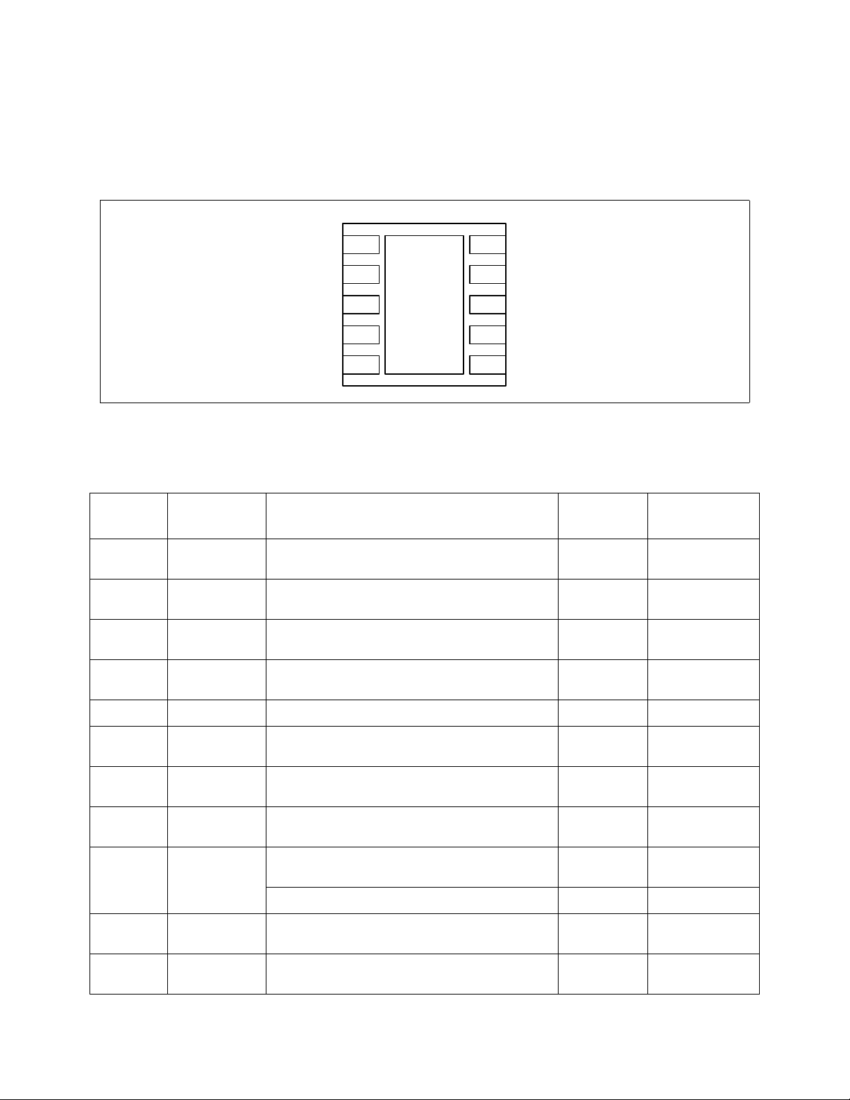
Figure 1.1 CAP1296-1 Pin Diagram (10-Pin 3 x 3 mm DFN) . . . . . . . . . . . . . . . . . . . . . . . . . . . . . . . . 8
Figure 3.1 SMBus Timing Diagram . . . . . . . . . . . . . . . . . . . . . . . . . . . . . . . . . . . . . . . . . . . . . . . . . . . 14
Figure 4.1 System Diagram for CAP1296 . . . . . . . . . . . . . . . . . . . . . . . . . . . . . . . . . . . . . . . . . . . . . . 19
Figure 4.2 POR and PORR With Slow Rising V
Figure 4.3 Signal Guard. . . . . . . . . . . . . . . . . . . . . . . . . . . . . . . . . . . . . . . . . . . . . . . . . . . . . . . . . . . . 23
Figure 4.4 Sensor Interrupt Behavior - Repeat Rate Enabled. . . . . . . . . . . . . . . . . . . . . . . . . . . . . . . 25
Figure 4.5 Sensor Interrupt Behavior - No Repeat Rate Enabled . . . . . . . . . . . . . . . . . . . . . . . . . . . . 26
Figure 6.1 CAP1296 Package Drawing - 10-Pin DFN 3mm x 3mm . . . . . . . . . . . . . . . . . . . . . . . . . . 60
Figure 6.2 CAP1296 Package Dimensions - 10-Pin DFN 3mm x 3mm. . . . . . . . . . . . . . . . . . . . . . . . 61
Figure 6.3 CAP1296 PCB Land Pattern and Stencil - 10-Pin DFN 3mm x 3mm. . . . . . . . . . . . . . . . . 61
Figure 6.4 CAP1296 PCB Detail A - 10-Pin DFN 3mm x 3mm . . . . . . . . . . . . . . . . . . . . . . . . . . . . . . 62
Figure 6.5 CAP1296 PCB Detail B - 10-Pin DFN 3mm x 3mm . . . . . . . . . . . . . . . . . . . . . . . . . . . . . . 63
Figure 6.6 CAP1296 Land Dimensions - 10-Pin DFN 3mm x 3mm. . . . . . . . . . . . . . . . . . . . . . . . . . . 63
Figure 6.7 CAP1296-1 Package Marking . . . . . . . . . . . . . . . . . . . . . . . . . . . . . . . . . . . . . . . . . . . . . . 64
and BOR with Falling V
DD
DD . . . . . . . . . . . . . . . . . . . . . . . 20
2013 Microchip Technology Inc. DS01569A-page 5
Page 6

6-Channel Capacitive Touch Sensor with Proximity Detection & Signal Guard
Datasheet
List of Tables
Table 1.1 Pin Description for CAP1296 . . . . . . . . . . . . . . . . . . . . . . . . . . . . . . . . . . . . . . . . . . . . . . . . 8
Table 1.2 Pin Types . . . . . . . . . . . . . . . . . . . . . . . . . . . . . . . . . . . . . . . . . . . . . . . . . . . . . . . . . . . . . . . 9
Table 2.1 Absolute Maximum Ratings . . . . . . . . . . . . . . . . . . . . . . . . . . . . . . . . . . . . . . . . . . . . . . . . 10
Table 2.2 Electrical Specifications . . . . . . . . . . . . . . . . . . . . . . . . . . . . . . . . . . . . . . . . . . . . . . . . . . . 11
Table 3.1 Protocol Format . . . . . . . . . . . . . . . . . . . . . . . . . . . . . . . . . . . . . . . . . . . . . . . . . . . . . . . . . 15
Table 3.2 Write Byte Protocol. . . . . . . . . . . . . . . . . . . . . . . . . . . . . . . . . . . . . . . . . . . . . . . . . . . . . . . 16
Table 3.3 Read Byte Protocol. . . . . . . . . . . . . . . . . . . . . . . . . . . . . . . . . . . . . . . . . . . . . . . . . . . . . . . 16
Table 3.4 Send Byte Protocol. . . . . . . . . . . . . . . . . . . . . . . . . . . . . . . . . . . . . . . . . . . . . . . . . . . . . . . 16
Table 3.5 Receive Byte Protocol. . . . . . . . . . . . . . . . . . . . . . . . . . . . . . . . . . . . . . . . . . . . . . . . . . . . . 16
Table 3.6 Block Read Protocol . . . . . . . . . . . . . . . . . . . . . . . . . . . . . . . . . . . . . . . . . . . . . . . . . . . . . . 17
Table 3.7 Block Write Protocol . . . . . . . . . . . . . . . . . . . . . . . . . . . . . . . . . . . . . . . . . . . . . . . . . . . . . . 17
Table 4.1 Ideal Base Counts. . . . . . . . . . . . . . . . . . . . . . . . . . . . . . . . . . . . . . . . . . . . . . . . . . . . . . . . 22
Table 5.1 Register Set in Hexadecimal Order . . . . . . . . . . . . . . . . . . . . . . . . . . . . . . . . . . . . . . . . . . 27
Table 5.2 Main Control Register. . . . . . . . . . . . . . . . . . . . . . . . . . . . . . . . . . . . . . . . . . . . . . . . . . . . . 30
Table 5.3 Power State Bit Overrides. . . . . . . . . . . . . . . . . . . . . . . . . . . . . . . . . . . . . . . . . . . . . . . . . . 30
Table 5.4 GAIN and C_GAIN Bit Decode. . . . . . . . . . . . . . . . . . . . . . . . . . . . . . . . . . . . . . . . . . . . . . 31
Table 5.5 Status Registers . . . . . . . . . . . . . . . . . . . . . . . . . . . . . . . . . . . . . . . . . . . . . . . . . . . . . . . . . 32
Table 5.6 Noise Flag Status Registers . . . . . . . . . . . . . . . . . . . . . . . . . . . . . . . . . . . . . . . . . . . . . . . . 33
Table 5.7 Sensor Input Delta Count Registers . . . . . . . . . . . . . . . . . . . . . . . . . . . . . . . . . . . . . . . . . . 34
Table 5.8 Sensitivity Control Register. . . . . . . . . . . . . . . . . . . . . . . . . . . . . . . . . . . . . . . . . . . . . . . . . 34
Table 5.9 DELTA_SENSE Bit Decode . . . . . . . . . . . . . . . . . . . . . . . . . . . . . . . . . . . . . . . . . . . . . . . . 35
Table 5.10 BASE_SHIFT Bit Decode . . . . . . . . . . . . . . . . . . . . . . . . . . . . . . . . . . . . . . . . . . . . . . . . . . 35
Table 5.11 Configuration Registers . . . . . . . . . . . . . . . . . . . . . . . . . . . . . . . . . . . . . . . . . . . . . . . . . . . 36
Table 5.12 Sensor Input Enable Register. . . . . . . . . . . . . . . . . . . . . . . . . . . . . . . . . . . . . . . . . . . . . . . 38
Table 5.13 Sensor Input Configuration Register. . . . . . . . . . . . . . . . . . . . . . . . . . . . . . . . . . . . . . . . . . 38
Table 5.14 MAX_DUR Bit Decode . . . . . . . . . . . . . . . . . . . . . . . . . . . . . . . . . . . . . . . . . . . . . . . . . . . . 38
Table 5.15 RPT_RATE Bit Decode. . . . . . . . . . . . . . . . . . . . . . . . . . . . . . . . . . . . . . . . . . . . . . . . . . . . 39
Table 5.16 Sensor Input Configuration 2 Register . . . . . . . . . . . . . . . . . . . . . . . . . . . . . . . . . . . . . . . . 40
Table 5.17 M_PRESS Bit Decode . . . . . . . . . . . . . . . . . . . . . . . . . . . . . . . . . . . . . . . . . . . . . . . . . . . . 40
Table 5.18 Averaging and Sampling Configuration Register . . . . . . . . . . . . . . . . . . . . . . . . . . . . . . . . 41
Table 5.19 AVG Bit Decode . . . . . . . . . . . . . . . . . . . . . . . . . . . . . . . . . . . . . . . . . . . . . . . . . . . . . . . . . 41
Table 5.20 SAMP_TIME Bit Decode. . . . . . . . . . . . . . . . . . . . . . . . . . . . . . . . . . . . . . . . . . . . . . . . . . . 42
Table 5.21 CYCLE_TIME Bit Decode. . . . . . . . . . . . . . . . . . . . . . . . . . . . . . . . . . . . . . . . . . . . . . . . . . 42
Table 5.22 Calibration Activate and Status Register . . . . . . . . . . . . . . . . . . . . . . . . . . . . . . . . . . . . . . 42
Table 5.23 Interrupt Enable Register . . . . . . . . . . . . . . . . . . . . . . . . . . . . . . . . . . . . . . . . . . . . . . . . . . 43
Table 5.24 Repeat Rate Enable Register . . . . . . . . . . . . . . . . . . . . . . . . . . . . . . . . . . . . . . . . . . . . . . . 44
Table 5.25 Signal Guard Enable Register . . . . . . . . . . . . . . . . . . . . . . . . . . . . . . . . . . . . . . . . . . . . . . 45
Table 5.26 Multiple Touch Configuration . . . . . . . . . . . . . . . . . . . . . . . . . . . . . . . . . . . . . . . . . . . . . . . 45
Table 5.27 B_MULT_T Bit Decode. . . . . . . . . . . . . . . . . . . . . . . . . . . . . . . . . . . . . . . . . . . . . . . . . . . . 46
Table 5.28 Multiple Touch Pattern Configuration . . . . . . . . . . . . . . . . . . . . . . . . . . . . . . . . . . . . . . . . . 46
Table 5.29 MTP_TH Bit Decode. . . . . . . . . . . . . . . . . . . . . . . . . . . . . . . . . . . . . . . . . . . . . . . . . . . . . . 47
Table 5.30 Multiple Touch Pattern Register . . . . . . . . . . . . . . . . . . . . . . . . . . . . . . . . . . . . . . . . . . . . . 47
Table 5.31 Base Count Out of Limit Register . . . . . . . . . . . . . . . . . . . . . . . . . . . . . . . . . . . . . . . . . . . . 48
Table 5.32 Recalibration Configuration Registers . . . . . . . . . . . . . . . . . . . . . . . . . . . . . . . . . . . . . . . . 48
Table 5.33 NEG_DELTA_CNT Bit Decode. . . . . . . . . . . . . . . . . . . . . . . . . . . . . . . . . . . . . . . . . . . . . . 49
Table 5.34 CAL_CFG Bit Decode. . . . . . . . . . . . . . . . . . . . . . . . . . . . . . . . . . . . . . . . . . . . . . . . . . . . . 50
Table 5.35 Sensor Input Threshold Registers . . . . . . . . . . . . . . . . . . . . . . . . . . . . . . . . . . . . . . . . . . . 50
Table 5.36 Sensor Input Noise Threshold Register . . . . . . . . . . . . . . . . . . . . . . . . . . . . . . . . . . . . . . . 51
Table 5.37 CSx_BN_TH Bit Decode. . . . . . . . . . . . . . . . . . . . . . . . . . . . . . . . . . . . . . . . . . . . . . . . . . . 51
Table 5.38 Standby Channel Register . . . . . . . . . . . . . . . . . . . . . . . . . . . . . . . . . . . . . . . . . . . . . . . . . 51
Table 5.39 Standby Configuration Register . . . . . . . . . . . . . . . . . . . . . . . . . . . . . . . . . . . . . . . . . . . . . 52
Table 5.40 STBY_AVG Bit Decode . . . . . . . . . . . . . . . . . . . . . . . . . . . . . . . . . . . . . . . . . . . . . . . . . . . 52
DS01569A-page 6 2013 Microchip Technology Inc.
Page 7

6-Channel Capacitive Touch Sensor with Proximity Detection & Signal Guard
Datasheet
Table 5.41 STBY_SAMP_TIME Bit Decode. . . . . . . . . . . . . . . . . . . . . . . . . . . . . . . . . . . . . . . . . . . . . 53
Table 5.42 STBY_CY_TIME Bit Decode . . . . . . . . . . . . . . . . . . . . . . . . . . . . . . . . . . . . . . . . . . . . . . . 53
Table 5.43 Standby Sensitivity Register . . . . . . . . . . . . . . . . . . . . . . . . . . . . . . . . . . . . . . . . . . . . . . . . 54
Table 5.44 STBY_SENSE Bit Decode . . . . . . . . . . . . . . . . . . . . . . . . . . . . . . . . . . . . . . . . . . . . . . . . . 54
Table 5.45 Standby Threshold Register . . . . . . . . . . . . . . . . . . . . . . . . . . . . . . . . . . . . . . . . . . . . . . . . 54
Table 5.46 Sensor Input Base Count Registers . . . . . . . . . . . . . . . . . . . . . . . . . . . . . . . . . . . . . . . . . . 55
Table 5.47 Power Button Register . . . . . . . . . . . . . . . . . . . . . . . . . . . . . . . . . . . . . . . . . . . . . . . . . . . . 55
Table 5.48 PWR_BTN Bit Decode . . . . . . . . . . . . . . . . . . . . . . . . . . . . . . . . . . . . . . . . . . . . . . . . . . . . 56
Table 5.49 Power Button Configuration Register . . . . . . . . . . . . . . . . . . . . . . . . . . . . . . . . . . . . . . . . . 56
Table 5.50 Power Button Time Bits Decode. . . . . . . . . . . . . . . . . . . . . . . . . . . . . . . . . . . . . . . . . . . . . 57
Table 5.51 Sensor Input Calibration Registers. . . . . . . . . . . . . . . . . . . . . . . . . . . . . . . . . . . . . . . . . . . 57
Table 5.52 Calibration Sensitivity Configuration Registers. . . . . . . . . . . . . . . . . . . . . . . . . . . . . . . . . . 58
Table 5.53 CALSENX Bit Decode. . . . . . . . . . . . . . . . . . . . . . . . . . . . . . . . . . . . . . . . . . . . . . . . . . . . . 58
Table 5.54 Product ID Register. . . . . . . . . . . . . . . . . . . . . . . . . . . . . . . . . . . . . . . . . . . . . . . . . . . . . . . 58
Table 5.55 Vendor ID Register . . . . . . . . . . . . . . . . . . . . . . . . . . . . . . . . . . . . . . . . . . . . . . . . . . . . . . . 58
Table 5.56 Revision Register . . . . . . . . . . . . . . . . . . . . . . . . . . . . . . . . . . . . . . . . . . . . . . . . . . . . . . . . 59
Table A.1 Register Delta. . . . . . . . . . . . . . . . . . . . . . . . . . . . . . . . . . . . . . . . . . . . . . . . . . . . . . . . . . . 65
Table 6.1 Revision History . . . . . . . . . . . . . . . . . . . . . . . . . . . . . . . . . . . . . . . . . . . . . . . . . . . . . . . . . 67
2013 Microchip Technology Inc. DS01569A-page 7
Page 8
6-Channel Capacitive Touch Sensor with Proximity Detection & Signal Guard
CS3 / SG
CS2
1
2
3
4
5
CS4
CS1
ALERT#
SMDATA
VDD
SMCLK CS5
CS6
GND
10
9
8
7
6
Chapter 1 Pin Description
Figure 1.1 CAP1296-1 Pin Diagram (10-Pin 3 x 3 mm DFN)
Datasheet
Table 1.1 Pin Description for CAP1296
PIN # PIN NAME PIN FUNCTION PIN TYPE
1 CS1 Capacitive Touch Sensor Input 1 AIO
2ALERT#
3SMDATA
4SMCLK
5 VDD Positive Power supply Power n/a
6 CS6 Capacitive Touch Sensor Input 6 AIO
7 CS5 Capacitive Touch Sensor Input 5 AIO
8 CS4 Capacitive Touch Sensor Input 4 AIO
9 CS3 / SG
ALERT# - Active low alert / interrupt output for
SMBus alert - requires pull-up resistor (default)
SMDATA - Bi-directional, open-dra in SMBus or
2
C data - requires pull-up resistor
I
2
SMCLK - SMBus or I
CS3 - Capacitive Touch Sensor Input 3 AIO
SG - Signal guard output AIO Leave Open
C clock input - requires
pull-up resistor
OD
DIOD n/a
DI n/a
CONNECTION
Connect to
Connect to
Connect to
Connect to
Connect to
Connect to
UNUSED
Ground
Ground
Ground
Ground
Ground
Ground
10 CS2 Capacitive Touch Sensor Input 2 AIO
Bottom
Pad
DS01569A-page 8 2013 Microchip Technology Inc.
GND Ground Power n/a
Connect to
Ground
Page 9

6-Channel Capacitive Touch Sensor with Proximity Detection & Signal Guard
Datasheet
APPLICATION NOTE: All digital pins are 5V tolerant pins.
The pin types are described in Table1.2.
Table 1.2 Pin Types
PIN TYPE DESCRIPTION
Power This pin is used to supply power or ground to th e device.
DI Digital Input - This pin is used as a digital input. This pin is 5V tolerant.
AIO Analog Input / Output - This pin is used as an I/O for analog signals.
DIOD
OD
Digital Input / Open Drain Output - This pin is used as a digital I/O. When it is used as an
output, it is open drain and requires a pull-up resistor. This pin is 5V tolerant.
Open Drain Digital Output - This pin is used as a digital output. It is open drain and requires
a pull-up resistor. This pin is 5V tolerant.
2013 Microchip Technology Inc. DS01569A-page 9
Page 10

6-Channel Capacitive Touch Sensor with Proximity Detection & Signal Guard
Chapter 2 Electrical Specifications
Table 2.1 Absolute Maximum Ratings
Voltage on VDD pin -0.3 to 6.5 V
Voltage on CS pins to GND -0.3 to 4.0 V
Datasheet
Voltage on 5V tolerant pins (V
Voltage on 5V tolerant pins (|V
Input current to any pin except VDD +
) -0.3 to 5.5 V
5VT_PIN
- VDD|) (see Note 2.2)0 to 3.6 V
5VT_PIN
10 mA
Output short circuit current Continuous N/A
Package Power Dissipation up to TA = 85°C for 10-pin DFN
0.5 W
(see Note 2.3)
Junction to Ambient (θ
) (see Note 2.4)78 °C/W
JA
Operating Ambient Temperature Range -40 to 125 °C
Storage Temperature Range -55 to 150 °C
ESD Rating, All Pins, HBM 8000 V
Note 2.1 Stresses above those listed could cause permanent damage to the device. This is a stress
rating only and functional operation of the device at any other condition above those
indicated in the operation sections of this specification is not implied.
Note 2.2 For the 5V tolerant pins that have a pull-up resistor, the voltage difference between
V
and VDD must never exceed 3.6V.
5VT_PIN
Note 2.3 The Package Power Dissipation specification assumes a recommended thermal via design
consisting of a 2x3 matrix of 0.3mm (12mil) vias at 0.9mm pitch conn ected to the ground
plane with a 1.6 x 2.3mm thermal landing.
Note 2.4 Junction to Ambient (θ
) is dependent on the design of the thermal vias. Without thermal
JA
vias and a thermal landing, the θJA will be higher.
DS01569A-page 10 2013 Microchip Technology Inc.
Page 11

6-Channel Capacitive Touch Sensor with Proximity Detection & Signal Guard
Datasheet
Table 2.2 Electrical Specifications
VDD = 3V to 5.5V, TA = 0°C to 85°C, all Typical values at TA = 25°C unless otherwise noted.
CHARACTERISTIC SYMBOL MIN TYP MAX UNIT CONDITIONS
DC POWER
Supply Voltage V
Supply Current
Maximum Base
Capacitance
Minimum Detectable
Capacitive Shift
DD
I
STBY_DEF
I
STBY_LP
I
DSLEEP_3V
I
DSLEEP_5V
I
DD
C
BASE
ΔC
TOUCH
3.0 5.5 V
Standby state active
120 170 µA
1 sensor input monitored
Default conditions (8 avg, 70ms
cycle time)
Standby state active
50 µA
1 sensor input monitored
1 avg, 140ms cycle time
Deep Sleep state active
5TBDµA
No communications
T
< 40°C
A
3.135 < V
< 3.465V
DD
Deep Sleep state active
TBD TBD µA
500 750 µA
No communications
T
< 40°C
A
V
= 5V
DD
Capacitive Sensing Active
signal guard disabled
CAPACITIVE TOUCH SENSOR INPUTS
50 pF Pad untouched
20 fF Pad touched - defaul t conditions
Recommended Cap
Shift
ΔC
TOUCH
0.1 2 pF Pad touched - Not tested
Untouched Current Counts
Power Supply
Rejection
PSR ±3 ±10
counts
/ V
Base Capacitance 5pF - 50pF
Negative Delta Counts disabled
Maximum sensitivity
All other parameters default
POWER-ON AND BROWN-OUT RESET (SEE Section 4.2, "Reset")
Power-On Reset
Voltage
Power-On Reset
Release Voltage
Brown-Out Reset V
V
V
PORR
POR
BOR
1 1.3 V Pin States Defined
2.85 V
Rising V
Ensured by design
2.8 V Falling V
DD
DD
VDD Rise Rate
(ensures internal
POR signal)
2013 Microchip Technology Inc. DS01569A-page 11
SV
DD
0.05 V/ms 0 to 3V in 60ms
Page 12

6-Channel Capacitive Touch Sensor with Proximity Detection & Signal Guard
Table 2.2 Electrical Specifications (continued)
V
= 3V to 5.5V, TA = 0°C to 85°C, all Typical values at TA = 25°C unless otherwise noted.
DD
CHARACTERISTIC SYMBOL MIN TYP MAX UNIT CONDITIONS
Datasheet
Power-Up Timer
Period
Brown-Out Reset
Voltage Delay
t
t
BORDC
Time to
Communications
Ready
Time to First
Conversion Ready
t
COMM_DLY
t
CONV_DLY
Output Low Voltage V
Output High Voltage V
Input High Voltage V
Input Low Voltage V
Leakage Current I
PWRT
OL
OH
IH
IL
LEAK
10 ms
1µsV
DD
= V
BOR
- 1
TIMING
15 ms
170 200 ms
I/O PINS
VDD -
0.4
0.4 V I
VI
SOURCE_IO
SINK_IO
= 8mA
= 8mA
2.0 V
0.8 V
powered or unpowered
T
< 85°C
±5 µA
pull-up voltage <
A
3.6V if
unpowered
SG PIN
Capacitive Drive
Capability
C
BASE_SG
20 200 pF capacitance to ground
SMBUS TIMING
Input Capacitance C
Clock Frequency f
Spike Suppression t
Bus Free Time Stop
to Start
Start Setup Time t
Sta rt Ho ld Ti me t
Stop Setup Time t
Data Hold Time t
Data Hold Time t
Data Setup Time t
DS01569A-page 12 2013 Microchip Technology Inc.
IN
SMB
SP
t
BUF
SU:STA
HD:STA
SU:STO
HD:DAT
HD:DAT
SU:DAT
10 400 kHz
1.3 µs
0.6 µs
0.6 µs
0.6 µs
0 µs When transmitting to the master
0.3 µs When receiving from the master
0.6 µs
5pF
50 ns
Page 13

6-Channel Capacitive Touch Sensor with Proximity Detection & Signal Guard
Datasheet
Table 2.2 Electrical Specifications (continued)
VDD = 3V to 5.5V, TA = 0°C to 85°C, all Typical values at TA = 25°C unless otherwise noted.
CHARACTERISTIC SYMBOL MIN TYP MAX UNIT CONDITIONS
Clock Low Period t
Clock High Period t
Clock / Data Fall
Time
Clock / Data Rise
Time
Capacitive Load C
LOW
HIGH
t
FALL
t
RISE
LOAD
1.3 µs
0.6 µs
300 ns Min = 20+0.1C
300 ns Min = 20+0.1C
400 pF per bus line
LOAD
LOAD
ns
ns
2013 Microchip Technology Inc. DS01569A-page 13
Page 14
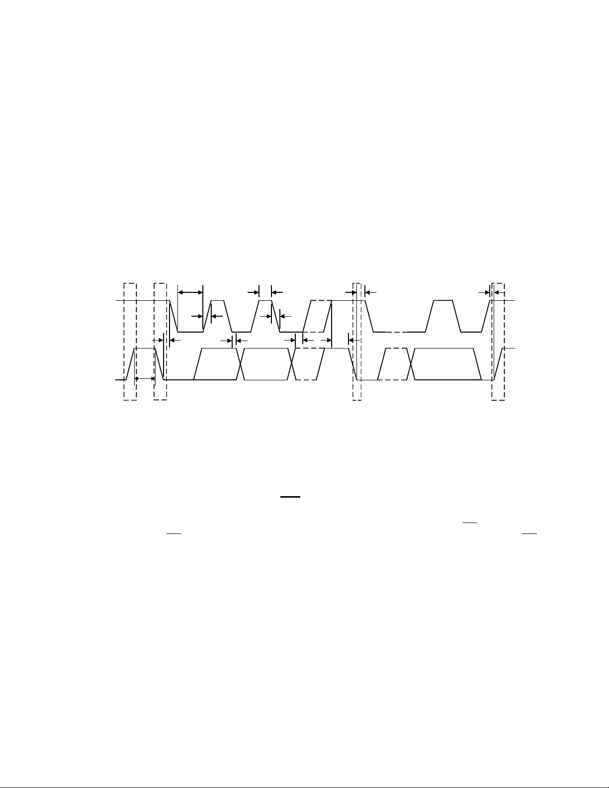
6-Channel Capacitive Touch Sensor with Proximity Detection & Signal Guard
SMDATA
SMCLK
T
BUF
P
S
S - Start Condition
P - Stop Condition
PS
T
HIGH
T
LOW
T
HD:STA
T
SU:STO
T
HD:STA
T
HD:DAT
T
SU:DAT
T
SU:STA
T
FALL
T
RISE
Chapter 3 Communications
3.1 Communications
The CAP1296 communicates using the SMBus or I2C protocol.
3.2 System Management Bus
The CAP1296 communicates with a host controller, such as an MCHP SIO, through the SMBus. The
SMBus is a two-wire serial communication protocol between a computer host and its peripheral
devices. A detailed timing diagram is shown in Figure 3.1. Stretching of the SMCLK signal is supported;
however, the CAP1296 will not stretch the clock signal.
Datasheet
Figure 3.1 SMBus Timing Diagram
3.2.1 SMBus Start Bit
The SMBus Start bit is defined as a transition of the SMBus Data line from a logic ‘1’ state to a logic
‘0’ state while the SMBus Clock line is in a logic ‘1’ state.
3.2.2 SMBus Address and RD / WR Bit
The SMBus Address Byte consists of the 7-bit client address followed by the RD / WR indicator bit. If
this RD / WR bit is a logic ‘0’, then the SMBus Host is writing data to the client device. If this RD / WR
bit is a logic ‘1’, then the SMBus Host is reading data from the client device.
The CAP1296 responds to SMBus address 0101_000(r/w).
3.2.3 SMBus Data Bytes
All SMBus Data bytes are sent most significant bit first and composed of 8-bits of information.
3.2.4 SMBus ACK and NACK Bits
The SMBus client will acknowledge all data bytes that it receives. This is done by the cl ient device
DS01569A-page 14 2013 Microchip Technology Inc.
pulling the SMBus Data line low after the 8th bit of each byte that is transmitted. This applies to both
the Write Byte and Block Write protocols.
The Host will NACK (not acknowledge) the last data byte to be received from the client by holding the
SMBus data line high after the 8th data bit has been sent. For the Block Read protocol, the Host will
ACK each data byte that it receives except the last data byte.
Page 15

6-Channel Capacitive Touch Sensor with Proximity Detection & Signal Guard
Datasheet
3.2.5 SMBus Stop Bit
The SMBus Stop bit is defined as a transition of the SMBus Data line from a logic ‘0’ state to a logic
‘1’ state while the SMBus clock line is in a logic ‘1’ state. When the CAP1296 detects an SMBus Stop
bit and it has been communicating with the SMBus protocol, it will reset its client interface and prepare
to receive further communications.
3.2.6 SMBus Timeout
The CAP1296 includes an SMBus timeout feature. Following a 30ms period of inactivity on the SMBus
where the SMCLK pin is held low, the device will timeout and reset the SMBus interface.
The timeout function defaults to disabled. It can be enabled by setting the TIMEOUT bit in the
Configuration register (see Section 5.6, "Configuration Registers").
3.2.7 SMBus and I2C Compatibility
The major differences between SMBus and I2C devices are highlighted here. For more information,
refer to the SMBus 2.0 specification.
1. CAP1296 supports I
2. Minimum frequency for SMBus communications is 10kHz.
2
C fast mode at 400kHz. This covers the SMBus max time of 100kHz.
3. The SMBus client protocol will reset if the clock is held low longer than 30ms (timeout condition).
This can be enabled in the CAP1296 by setting the TIMEOUT bit in the Configuration register. I2C
does not have a timeout.
4. The SMBus client protocol will reset if both the clock and the data line are high for longer than
200us (idle condition). This can be enabled in the CAP1296 by setting the TIMEOUT bit in the
Configuration register. I
2
5. I
C devices do not support the Alert Response Address functionality (which is op tional for SMBus).
2
C devices support block read and write differently. I2C protocol allows for unlimited number of
6. I
bytes to be sent in either direction. The SMBus protocol requires that an additional data byte
indicating number of bytes to read / write is transmitted. The CAP1296 supports I
2
C does not have an idle condition.
3.3 SMBus Protocols
The CAP1296 is SMBus 2.0 compatible and supports Write Byte, Read Byte, Send Byte, and Receive
Byte as valid protocols as shown below.
All of the below protocols use the convention in Table 3.1.
DATA SENT
TO DEVICE
Data sent Data sent
Table 3.1 Protocol Format
DATA SENT TO
THE HOST
2
C formatting only .
2013 Microchip Technology Inc. DS01569A-page 15
Page 16

3.3.1 SMBus Write Byte
The Write Byte is used to write one byte of data to a specific register as shown in Table 3.2.
6-Channel Capacitive Touch Sensor with Proximity Detection & Signal Guard
Datasheet
Table 3.2 Write Byte Protocol
START
SLAVE
ADDRESS WR
ACK
REGISTER
ADDRESS ACK
REGISTER
DATA ACK STOP
1 ->0 0101 _000 0 0 XXh 0 XXh 0 0 -> 1
3.3.2 SMBus Read Byte
The Read Byte protocol is used to read one byte of data from the registers as show n in Table 3.3.
Table 3.3 Read Byte Protocol
START SLAVE
ADDRESS
WR ACK REGISTER
ADDRESS
ACK START CLIENT
ADDRESS
RD ACK REGISTER
DATA
NACK STOP
1->0 0101_000 0 0 XXh 0 1 ->0 0 101_000 1 0 XXh 1 0 -> 1
3.3.3 SMBus Send Byte
The Send Byte protocol is used to set the internal address register pointer to the correct address
location. No data is transferred during the Send Byte protocol as shown in Table 3.4.
APPLICATION NOTE: The Send Byte protocol is not functional in Deep Sleep (i.e., DSLEEP bit is set).
Table 3.4 Send Byte Protocol
START
SLAVE
ADDRESS WR ACK
REGISTER
ADDRESS ACK STOP
1 -> 0 0101_000 0 0 XXh 0 0 -> 1
3.3.4 SMBus Receive Byte
The Receive Byte protocol is used to read data from a register when the internal register address
pointer is known to be at the right location (e.g. set via Send Byte). This is used for consecutive reads
of the same register as shown in Table 3.5.
APPLICATION NOTE: The Receive Byte protocol is not functional in Deep Sleep (i.e., DSLEEP bit is set).
Table 3.5 Receive Byte Protocol
SLAVE
START
1 -> 0 0101_000 1 0 XXh 1 0 -> 1
DS01569A-page 16 2013 Microchip Technology Inc.
ADDRESS RD
ACK REGISTER DATA NACK STOP
Page 17

6-Channel Capacitive Touch Sensor with Proximity Detection & Signal Guard
Datasheet
3.4 I2C Protocols
The CAP1296 supports I2C Block Read and Block Write.
The protocols listed below use the convention in Table 3.1.
3.4.1 Block Read
The Block Read is used to read multiple data bytes from a group of contiguous registers as sh own in
Table 3.6.
APPLICATION NOTE: When using the Block Read protocol, the internal address pointer will be automatically
incremented after every data byte is received. It will wrap from FFh to 00h.
Table 3.6 Block Read Protocol
START SLAVE
ADDRESS
WR ACK REGISTER
ADDRESS
ACK START SLAVE
ADDRESS
RD ACK REGISTER
DATA
1->0 0101_000 0 0 XXh 0 1 ->0 0101_000 1 0 XXh
ACK REGISTER
DATA
ACK REGISTER
DATA
ACK REGISTER
DATA
ACK . . . REGISTER
DATA
NACK STOP
0 XXh 0 XXh 0 XXh 0 . . . XXh 1 0 -> 1
3.4.2 Block Write
The Block Write is used to write multiple data bytes to a group of contiguous registers as shown in
Table 3.7.
APPLICATION NOTE: When using the Block Write protocol, the internal address pointer will be automatically
incremented after every data byte is received. It will wrap from FFh to 00h.
Table 3.7 Block Write Protocol
REGISTER
ADDRESS ACK
START
SLAVE
ADDRESS WR
ACK
1 ->0 0101_000 0 0 XXh 0 XXh 0
REGISTER
DATA
ACK
REGISTER
DATA ACK . . .
REGISTER
DATA ACK STOP
REGISTER
DATA ACK
XXh 0 XXh 0 . . . XXh 0 0 -> 1
2013 Microchip Technology Inc. DS01569A-page 17
Page 18

6-Channel Capacitive Touch Sensor with Proximity Detection & Signal Guard
Chapter 4 General Description
The CAP1296 is a multiple channel capacitive touch sensor. It contains six (6) individual capacitive
touch sensor inputs with programmable sensitivity for use in touch sensor applications. Each sensor
input is calibrated to compensate for system parasitic capacitance and automatically recalibrated to
compensate for gradual environmental changes.
In addition, the CAP1296 can be configured to detect proximity on one or more channels with an
optional signal guard to reduce noise sensitivity.
The CAP1296 includes Multiple Pattern Touch recognition that allows the user to select a specific set
of buttons to be touched simultaneously. If this pattern is detected, a status bit is set and an interrupt
is generated.
The CAP1296 has Active and Standby states, each with its own sensor input configuration controls.
The Combo state allows a combination of sensor input controls to be used which enab les one or more
sensor inputs to operate as buttons while another sensor input is operating as a proximity detector.
Power consumption in the Standby and Combo states is dependent on the number of sensor inputs
enabled as well as averaging, sampling time, and cycle time. Deep Sleep is the lowest power state
available, drawing 5µA (typical) of current. In this state, no sensor inputs are active, and
communications will wake the device.
The device communicates with a host controller using SMBus / I
device for updated information at any time or it may configure the device to flag an in terrupt whenever
a touch is detected on any sensor pad.
Datasheet
2
C. The host controller may poll the
A typical system diagram is shown in Figure 4.1.
DS01569A-page 18 2013 Microchip Technology Inc.
Page 19

6-Channel Capacitive Touch Sensor with Proximity Detection & Signal Guard
CAP1296
CS4
SMDATA
SMCLK
Embedded
Controller
3.0V to 5.5V
ALERT#
CS5
CS6
CS2
CS1
Touch
Button
Touch
Button
Touch
Button
Proximity
Sensor
Touch
Button
SG*
VDDGND
* CS3 / SG is a multi-function pin. If not
using the signal guard sh own here, CS3
can be another touch button.
10kOhm
resistors
3.0V to 5.5V
1.0uF0.1uF
Datasheet
Figure 4.1 System Diagram for CAP1296
4.1 Power States
The CAP1296 has 4 power states depending on the status of the STBY, COMBO, and DSLEEP bits
(see Section 5.1, "Main Control Register"). When the device transitions between power states,
previously detected touches (for channels that are being de-activated) a re cleared a nd the sensor i nput
status bits are reset.
1. Active - The normal mode of operation. The device is monitoring capacitive sensor inputs enabled
in the Active state (see Section 5.7, "Sensor Input Enable Register").
2. Standby - When the STBY bit is set, the device is monitoring the capacitive sensor in puts enabled
in the Standby state (see Section 5.22, "Standby Channel Register"). Interrupts can still be
generated based on the enabled channels. The device will still respond to communications
normally and can be returned to the Active state of operation by clearing the STBY bit. Power
consumption in this state is dependent on the number of sensor inputs enabled as well as
averaging, sampling time, and cycle time.
3. Combo - When the COMBO bit is set, the device is monitoring capacitive sensor inputs enabled
in the Active state as well as inputs enabled in the Standby state (hence the name “Combo”).
Interrupts can still be generated based on the enabled channels. The device wi ll still respond to
communications normally and can be returned to the Active state of operation by clearing the
COMBO bit. Power consumption in this state is dependent on the number of sensor inputs enabled
as well as averaging, sampling time, and cycle time.
2013 Microchip Technology Inc. DS01569A-page 19
Page 20

4. Deep Sleep - When the DSLEEP bit is set, the device is in its lowest power state. It is not
V
DD
V
BOR
T
PWRT
GND
Undefined
SYSRST
V
POR
V
PORR
T
BORDCTPWRT
monitoring any capacitive sensor inputs. While in Deep Sleep, the CAP1296 can be awakened by
SMBus communications targeting the device. This will not cause the DSLEEP to be cleared so the
device will return to Deep Sleep once all communications have stopped. The device can be
returned to the Active state of operation by clearing the DSLEEP bit.
4.2 Reset
The Power-On Reset (POR) circuit holds the device in reset until VDD has reached an acceptable level,
Power-on Reset Release Voltage (V
used to extend the start-up period until all device operation conditions have been met. Th e power-up
timer starts after V
The Brown-Out Reset (BOR) circuit holds the device in reset when V
for longer than the BOR reset delay (t
up timer is started again and must finish before reset is released, as shown in Figure 4.2.
reaches V
DD
6-Channel Capacitive Touch Sensor with Proximity Detection & Signal Guard
Datasheet
), for minimum operation. The power-up timer (PWRT) is
PORR
. POR and PORR with slow rising VDD is shown in Figure 4.2.
PORR
falls to a minimum level, V
). After a BOR, when VDD rises above V
BORDC
DD
PORR
, the power-
BOR
Figure 4.2 POR and PORR With Slow Rising V
and BOR with Falling V
DD
DD
4.3 Capacitive Touch Sensing
The CAP1296 contains six (6) independent capacitive touch sensor inputs. Each sensor input has
dynamic range to detect a change of capacitance due to a touch. Additionally, each sensor input can
be configured to be automatically and routinely recalibrated.
4.3.1 Capacitive Touch Sensing Settings
Controls for managing capacitive touch sensor inp uts are determined by the power state.
4.3.1.1 Active State Sensing Settings
The Active state is used for normal operation. Sensor inputs being monitored are determined by the
Sensor Input Enable Register (see Section 5.7, "Sensor Input Enable Register"). Sensitivity is
controlled by the Sensitivity Control Register (see Section 5.5, "Sensitivity Control Register").
Averaging, sample time, and cycle time are controlled by the Averaging and Sampling Configuration
Register (see Section 5.10, "Averaging and Sampling Configuration Register"). Each channel can have
a separate touch detection threshold, as defined in the Sensor Input Threshold registers (see Section
5.20, "Sensor Input Threshold Registers").
4.3.1.2 Standby State Sensing Settings
The Standby state is used for standby operation. In general, fewer sensor inputs are enabled, and they
are programmed to have more sensitivity. Sensor inputs being monitored are determined by the
Standby Channel Register (see Section 5.22, "Standby Channel Register"). Sensitivity is controlled by
DS01569A-page 20 2013 Microchip Technology Inc.
Page 21

6-Channel Capacitive Touch Sensor with Proximity Detection & Signal Guard
Datasheet
the Standby Sensitivity Register (see Section 5.24, "Standby Sensitivity Register"). Averaging, sample
time, and cycle time are controlled by the Averaging and Sampling Configuration Register (see Section
5.23, "Standby Configuration Register"). There is one touch detection threshold, which applies to all
sensors enabled in Standby, as defined in the Standby Threshold Register (see Section 5.25, "Standby
Threshold Register").
4.3.1.3 Combo State Sensing Settings
The Combo state is used when a combination of proximity detection and norm al button operation is
required. When the COMBO bit is set, the sensing cycle includes sensor inputs enabled in the Active
state as well as sensor inputs enabled in the Standby state. Sensor inputs enabled in the Active state
will use the Active settings described in Section 4.3.1.1, "Active State Sensing Settings". Sensor inputs
enabled in the Standby state will use the Standby settings described in Section 4.3.1.2, "Standby State
Sensing Settings". If a sensor input is enabled in both th e Active state and in the Standby state, the
Active state settings will be used in Combo state. The programmed cycle time is determined by
STBY_CY_TIME[1:0].
The Combo state also has two gain settings. When the COMBO bit is set, the GAIN[1:0] control only
applies to the sensors enabled in the Active state, and the C_GAIN[1:0] control applies to the sensors
enabled in the Standby state.
4.3.2 Sensing Cycle
Except when in Deep Sleep, the device automatically initiates a sensing cycle and repeats the cycle
every time it finishes. The cycle polls through each enabled sensor input starting with CS1 and
extending through CS6. As each capacitive touch sensor i nput is polled, its measurement is compared
against a baseline “not touched” measurement. If the delta measurement is large enou gh to exceed
the applicable threshold, a touch is detected and an interrupt can be generated (see Section 4.9.2,
"Capacitive Sensor Input Interrupt Behavior").
The sensing cycle time is programmable (see Section 5.10, "Averaging and Sampling Configuration
Register" and Section 5.23, "Standby Configuration Register"). If all enabled inputs can be sampled in
less than the cycle time, the device is placed into a lower power state for the remainder of the sensi ng
cycle. If the number of active sensor inputs cannot be sampled within the specified cycle time, the
cycle time is extended and the device is not placed in a lower power state.
4.4 Sensor Input Calibration
Calibration sets the Base Count Registers (Section 5.26, "Sensor Input Base Count Registers") which
contain the “not touched” values used for touch detection comparisons. Calibration automatically
occurs after a power-on reset (POR), when sample time is changed, when the gain is changed, when
the calibration sensitivity is changed, and whenever a sensor input is newly enabled (for example,
when transitioning from a power state in which it was disabled to a power state in which it is enab led).
During calibration, the analog sensing circuits are tuned to the capacitance of the untouched pad.
Then, samples are taken from each sensor input so that a base count can be established. After
calibration, the untouched delta counts are zero.
APPLICATION NOTE: During the calibration routine, the sensor inputs will not detect a press for up to 200ms and
the Sensor Base Count Register values will be invalid. In addition, any press on the
corresponding sensor pads will invalidate the calibration.
The host controller can force a calibration for selected sensor inputs at any time using the Calibrati on
Activate and Status Register (Section 5.11, "Calibration Activate and Status Register"). When a bit is
set, the corresponding capacitive touch sensor input will be calibrated (both analog and digital). The
bit is automatically cleared once the calibration routine has successfully finished.
If analog calibration fails for a sensor input, the corresponding bit is not cleared in the Calibration
Activate and Status Register, and the ACAL_FAIL bit is set in the General Status Register (Section 5.2,
"Status Registers"). An interrupt can be generated. Analog calibration will fail if a noise bit is set or if
2013 Microchip Technology Inc. DS01569A-page 21
Page 22

6-Channel Capacitive Touch Sensor with Proximity Detection & Signal Guard
Datasheet
the calibration value is at the maximum or minimum value. If digital calibrati on fails to generate base
counts for a sensor input in the operating range, which is +12.5% from the ideal base count (see
Table 4.1), indicating the base capacitance is out of range, the corresponding BC_OUTx bit is set in
the Base Count Out of Limit Register (Section 5.18, "Base Count Out of Limit Register"), and the
BC_OUT bit is set in the General Status Register (Section 5.2, "Status Registers"). An interrupt can
be generated. By default, when a base count is out of limit, analog calibration is repeated for the
sensor input; alternatively, the sensor input can be sampled using the out of limit base count (Section
5.6, "Configuration Registers"). Calibration sensitivity can be ad justed for each sensor input based on
capacitive touch pad capacitance.
Table 4.1 Ideal Base Counts
IDEAL BASE COUNT SAMPLE TIME
3,200 320us
6,400 640us
12,800 1.28ms
25,600 2.56ms
During normal operation there are various options for reca librating the capacitive touch sensor inputs.
Recalibration is a digital adjustment of the base counts so that the untouched delta count is zero. After
a recalibration, if a sensor input’s base count has shifted +
calibration will be performed on the sensor input.
12.5% from the ideal base count, a full
4.4.1 Automatic Recalibration
Each sensor input is regularly recalibrated at a programmable rate (see CAL_CFG[2:0] in Section 5.19,
"Recalibration Configuration Register"). By default, the recalibration routine stores the average 64
previous measurements and periodically updates the base “not touched” setting for the capacitive
touch sensor input.
APPLICATION NOTE: Automatic recalibration only works when the delta count is below the active sensor input
threshold. It is disabled when a touch is detected.
4.4.2 Negative Delta Count Recalibration
It is possible that the device loses sensitivity to a touch. This may happen as a result of a noisy
environment, recalibration when the pad is touched but delta counts do not exceed the threshold, or
other environmental changes. When this occurs, the base untouched sensor input may generate
negative delta count values. The NEG_DELTA_CNT[1:0] bits (see Section 5.19, "Recalibration
Configuration Register") can be set to force a recalibration after a specified number of consecutive
negative delta readings. After a delayed recalibration (see Section 4.4.3, "Delayed Recalibration") the
negative delta count recalibration can correct after the touch is released.
APPLICATION NOTE: During this recalibration, the device will not respond to touches.
4.4.3 Delayed Recalibration
It is possible that a “stuck button” occurs when some thing is placed on a butto n which causes a touch
to be detected for a long period. By setting the MAX_DUR_EN bit (see Section 5.6, "Configuration
Registers"), a recalibration can be forced when a touch is held on a button for longer than the duration
specified in the MAX_DUR[3:0] bits (see Section 5.8, "Sensor Input Configuration Register").
DS01569A-page 22 2013 Microchip Technology Inc.
Page 23

6-Channel Capacitive Touch Sensor with Proximity Detection & Signal Guard
CAP129X Device
CS pin
SIGNAL_GUARD
CS pin
Touch Pad
Touch Pad
Datasheet
Note 4.1 Delayed recalibration only works when the delta count is above the active sensor input
threshold. If enabled, it is invoked when a sensor pad touch is held longer than the
MAX_DUR bit settings.
Note 4.2 For the power button, which requires that the button be held longer than a reg ular button,
the time specified by the MAX_DUR[3:0] bits is added to the time required to trigger the
qualifying event. This will prevent the power butto n from being recalibrated during the time
it is supposed to be held.
4.5 Proximity Detection
Each sensor input can be configured to detect changes in capacitance due to proximity of a touch.
This circuitry detects the change of capacitance that is generated as an object approaches, but does
not physically touch, the enabled sensor pad(s). Generally, sensor inputs used to detect proximity have
physically larger pads than standard buttons. In addition, gain should be increased to increase
sensitivity. To improve the signal, the signal guard feature ma y be used.
4.5.1 Signal Guard
The signal guard isolates the signal from virtual grounds, as shown in Figure 4.3. It can be used to
isolate the proximity antenna from nearby conductive surfaces tha t would otherwise attenuate the efield.
Figure 4.3 Signal Guard
4.6 Power Button
The CAP1296 has a “power button” feature. In general, buttons are set for quick response to a touch,
especially when buttons are used for number keypads. However, there are cases where a quick
response is not desired, such as when accidentally brushing the power button causes a device to turn
off or on unexpectedly.
The power button feature allows a sensor input to be designated as the “po wer button” (see Section
5.27, "Power Button Register"). The power button is configured so that a touch must be held on the
button for a designated period of time before an interrupt is generated; different times can be sel ected
for the Standby and the Active states (see Section 5.28, "Power Button Configuration Register"). The
feature can also be enabled / disabled for both states separately.
APPLICATION NOTE: For the power button feature to work in the Standby and/or Active states, the sensor input
must be enabled in the applicable state. If the power button feature is enabled for both
Standby and Active and the COMBO bit is set, the Standby power button settings will be
2013 Microchip Technology Inc. DS01569A-page 23
used.
Page 24

6-Channel Capacitive Touch Sensor with Proximity Detection & Signal Guard
After the designated power button has been held for the designated time, an interrupt is generated
and the PWR bit is set in the General Status Register (see Section 5.2, "Status Registers").
4.7 Multiple Touch Pattern Detection
The multiple touch pattern (MTP) detection circuitry can be used to detect lid closure or oth er similar
events. An event can be flagged based on either a minimum number of sensor i nputs or on specific
sensor inputs simultaneously exceeding an MTP threshold or having their Noise Fla g Status Register
bits set. An interrupt can also be generated. During an MTP event, all touches are blocked (see
Section 5.16, "Multiple Touch Pattern Configuration Register").
4.8 Noise Controls
4.8.1 Low Frequency Noise Detection
Each sensor input has a low frequency noise detector that will sense if low freque ncy noise is injected
onto the input with sufficient power to corrupt the readings. By default, if this occurs, the device will
reject the corrupted sample (see DIS_ANA_NOISE bit in Section 5.6.1, "Configuration - 20h") and the
corresponding bit is set to a logic ‘1’ in the Noise Flag Status register (see SHOW_RF_NOISE bit in
Section 5.6.2, "Configuration 2 - 44h").
Datasheet
4.8.2 RF Noise Detection
Each sensor input contains an integrated RF noise detector. This block will detect injected RF noise
on the CS pin. The detector threshold is dependent upon the noise frequency. By default, if RF noise
is detected on a CS line, that sample is removed and not compared against the threshold (see
DIS_RF_NOISE bit in Section 5.6.2, "Configuration 2 - 44h").
4.8.3 Noise Status and Configuration
The Noise Flag Status (see Section 5.3, "Noise Flag Status Registers") bits can be used to indicate
RF and/or other noise. If the SHOW_RF_NOISE bit in the Configuration Register (see Section 5.6,
"Configuration Registers") is set to 0, the Noise Flag Status bit for the capacitive sensor input is set if
any analog noise is detected. If the SHOW_RF_NOISE bit is set to 1, the Noise Flag Status bits will
only be set if RF noise is detected.
The CAP1296 offers optional noise filtering controls for both analog an d digital noise.
For analog noise, there are options for whether the data should be considered invalid. By default, the
DIS_ANA_NOISE bit (see Section 5.6.1, "Configuration - 20h") will block a touch on a sensor input if
low frequency analog noise is detected; the sample is discarded. By default, the DIS_RF_NOISE bit
(see Section 5.6.2, "Configuration 2 - 44h") will block a touch o n a sensor input if RF noise is detected;
the sample is discarded.
For digital noise, sensor input noise thresholds can be set (see Section 5.21, "Sensor Input Noise
Threshold Register"). If a capacitive touch sensor input exceeds the Sensor Noise Threshold but does
not exceed the touch threshold (Sensor Threshold (see Section 5.20, "Sensor Input Threshold
Registers") in the Active state or Sensor Standby Threshold in the Standby state (Section 5.25,
"Standby Threshold Register")), it is determined to be caused by a noise spike. The DIS_DIG_NOISE
bit (see Section 5.6.1, "Configuration - 20h") can be set to discard samples that indicate a noise spike
so they are not used in the automatic recalibration routine (see Section 4.4.1, "Automatic
Recalibration").
4.9 Interrupts
Interrupts are indicated by the setting of the INT bit in the Main Control Register (see Section 5.1,
"Main Control Register") and by assertion of the ALERT# pin. The ALERT# pin is cleared when the
DS01569A-page 24 2013 Microchip Technology Inc.
Page 25

6-Channel Capacitive Touch Sensor with Proximity Detection & Signal Guard
Touch Detected
INT bit
Button Status
Write to INT bit
Sensing Cycle
(35ms)
Min Press Setting
(280ms)
Interrupt on
Touch
Button Repeat Rate
(175ms)
Button Repeat Rate
(175ms)
Interrupt on
Release
(optional)
ALERT# pin
Datasheet
INT bit is cleared by the user. When the INT bit is cleared by the user, status bits may be cleared (see
Section 5.2, "Status Registers").
4.9.1 ALERT# Pin
The ALERT# pin is an active low output that is driven when an interrupt event is de tected.
4.9.2 Capacitive Sensor Input Interrupt Behavior
Each sensor input can be programmed to enable / disable interrupts (see Section 5.12, "Interrupt
Enable Register").
When enabled for a sensor input and the sensor input is not the designated power button, interrupts
are generated in one of two ways:
1. An interrupt is generated when a touch is detected and, as a user selectable option, when a release
is detected (by default - see INT_REL_n in Section 5.6.2, "Configuratio n 2 - 44h"). See Figure 4.5.
2. If the repeat rate is enabled then, so long as the touch is held, another interrupt will be generated
based on the programmed repeat rate (see Figure 4.4).
When the repeat rate is enabled for a sensor inpu t (see Section 5.13, "Repeat Rate Enable Register"),
the device uses an additional control called MPRESS that determines whether a touch is flagged as
a simple “touch” or a “press and hold” (see Section 5.9, "Sensor Input Configuration 2 Register"). The
MPRESS[3:0] bits set a minimum press timer. When the button is touched, the timer begins. If the
sensor pad is released before the minimum press timer expires, it is flagged as a touch and an
interrupt (if enabled) is generated upon release. If the sensor input detects a touch for longer than this
timer value, it is flagged as a “press and hold” event. So long as the touch is held, interrupts will be
generated at the programmed repeat rate (see Section 5.8, "Sensor Input Configuration Register") and
upon release (if enabled).
If a sensor input is the designated power button, an interrupt is not generated as soon as a touch is
detected and repeat rate is not applicable. See Section 4.9.3, "Inte rrupts for the Power Button".
APPLICATION NOTE: Figure 4.4 and Figure 4.5 show default operation which is to generate an interrupt upon
sensor pad release.
APPLICATION NOTE: The host may need to poll the device twice to dete rmine that a release has been detected.
Figure 4.4 Sensor Interrupt Behavior - Repeat Rate Enabled
2013 Microchip Technology Inc. DS01569A-page 25
Page 26

6-Channel Capacitive Touch Sensor with Proximity Detection & Signal Guard
Touch Detected
INT bit
Button Status
Write to INT bit
Sensing Cycle
(35ms)
Interrupt on
Touch
Interrupt on
Release
(optional)
ALERT# pin
Datasheet
Figure 4.5 Sensor Interrupt Behavior - No Repeat Rate Enabled
4.9.3 Interrupts for the Power Button
Interrupts are automatically enabled for the power button when the featu re is enabled (see Se ction 4 .6,
"Power Button"). A touch must be held on the power button for the designated period of time before
an interrupt is generated.
4.9.4 Interrupts for Multiple Touch Pattern Detectio n
An interrupt can be generated when the MTP pattern is matched (see Section 5.16, "Mul tiple Touch
Pattern Configuration Register").
4.9.5 Interrupts for Sensor Input Calibration Failures
An interrupt can be generated when the ACAL_FAIL bit is set, indicating the failure to complete analog
calibration of one or more sensor inputs (see Section 5.2, "Status Registers"). This interrupt can be
enabled by setting the ACAL_FAIL_INT bit (see Section 5.6, "Configuration Registers").
An interrupt can be generated when the BC_OUT bit is set, indicating the base count is o ut of limit for
one or more sensor inputs (see Section 5.2, "Status Registers"). This interrupt can be enabled by
setting the BC_OUT_INT bit (see Section 5.6, "Configuration Registers").
DS01569A-page 26 2013 Microchip Technology Inc.
Page 27

6-Channel Capacitive Touch Sensor with Proximity Detection & Signal Guard
Datasheet
Chapter 5 Register Description
The registers shown in Table 5.1 are accessible through the communications protocol. An entry of ‘-’
indicates that the bit is not used and will always read ‘0’.
Table 5.1 Register Set in Hexadecimal Order
REGISTER
ADDRESS R/W REGISTER NAME FUNCTION
00h R/W Main Control
02h R/W General Status Stores general status bits 00h Page 32
03h R Sensor Input Status
0Ah R Noise Flag Status
10h R
11h R
12h R
13h R
14h R
15h R
Sensor Input 1 Delta
Count
Sensor Input 2 Delta
Count
Sensor Input 3 Delta
Count
Sensor Input 4 Delta
Count
Sensor Input 5 Delta
Count
Sensor Input 6 Delta
Count
Controls power states and indicates
an interrupt
Returns the state of the sampled
capacitive touch sensor inputs
Stores the noise flags for sensor
inputs
Stores the delta count for CS1 00h Page 34
Stores the delta count for CS2 00h Page 34
Stores the delta count for CS3 00h Page 34
Stores the delta count for CS4 00h Page 34
Stores the delta count for CS5 00h Page 34
Stores the delta count for CS6 00h Page 34
DEFAULT
VALUE PAGE
00h Page 30
00h Page 32
00h Page 33
1Fh R/W Se nsitivity Control
20h R/W Configuration Controls general function ality 20h Page 36
21h R/W Sensor Input Enable
22h R/W
23h R/W
24h R/W
26h R/W
2013 Microchip Technology Inc. DS01569A-page 27
Sensor Input
Configuration
Sensor Input
Configuration 2
Averaging and
Sampling Config
Calibration Activate
and Status
Controls the sensitivity of the
threshold and delta counts and data
scaling of the base counts
Controls which sensor inputs are
monitored in Active
Controls max duration and auto-
repeat delay
Controls the MPRESS (“press and
hold”) setting
Controls averaging and sampling
window for Active
Forces calibration for capacitive
touch sensor inputs and indicates
calibration failure
2Fh Page 34
3Fh Page 38
A4h Page 38
07h Page 40
39h Page 41
00h Page 42
Page 28

6-Channel Capacitive Touch Sensor with Proximity Detection & Signal Guard
Table 5.1 Register Set in Hexa decimal Order (continued)
Datasheet
REGISTER
ADDRESS R/W REGISTER NAME FUNCTION
27h R/W Interrupt Enable
28h R/W Repeat Rate Enable
29h R/W Signal Guard Enable
2Ah R/W
2Bh R/W
Multiple Touch
Configuration
Multiple T ouch Pattern
Configuration
Determines which capacitive sensor
inputs can generate interrupts
Enables repeat rate for specific
sensor inputs
Enables the signal guard for specific
sensor inputs
Determines the number of
simultaneous touches to flag a
multiple touch condition
Determines the multiple touch
pattern (MTP) configuration
Determines the pattern or number of
2Dh R/W Multiple Touch Pattern
sensor inputs used by the MTP
circuitry
2Eh R
2Fh R/W
30h R/W
Base Count Out of
Limit
Recalibration
Configuration
Sensor Input 1
Threshold
Indicates whether sensor inputs
have a base count out of limit
Determines recalibration timing and
sampling window
Stores the touch detection threshold
for Active for CS1
DEFAULT
VALUE PAGE
3Fh Page 43
3Fh Page 44
00h Page 45
80h Page 45
00h Page 46
3Fh Page 47
00h Page 48
8Ah Page 48
40h Page 50
31h R/W
32h R/W
33h R/W
34h R/W
35h R/W
38h R/W
Sensor Input 2
Threshold
Sensor Input 3
Threshold
Sensor Input 4
Threshold
Sensor Input 5
Threshold
Sensor Input 6
Threshold
Sensor Input Noise
Threshold
Standby Configuration Registers
40h R/W Standby Channel
41h R/W Standby Configuration
42h R/W Standby Sensitivity
43h R/W Standby Threshold
Stores the touch detection threshold
for Active for CS2
Stores the touch detection threshold
for Active for CS3
Stores the touch detection threshold
for Active for CS4
Stores the touch detection threshold
for Active for CS5
Stores the touch detection threshold
for Active for CS6
Stores controls for selecting the
noise threshold for all sensor inputs
Controls which sensor inputs are
enabled for Standby
Controls averaging and sensing
cycle time for Standby
Controls sensitivity settings used for
Standby
Stores the touch detection threshold
for Standby
40h Page 50
40h Page 50
40h Page 50
40h Page 50
40h Page 50
01h Page 51
00h Page 51
39h Page 52
02h Page 54
40h Page 54
DS01569A-page 28 2013 Microchip Technology Inc.
Page 29

6-Channel Capacitive Touch Sensor with Proximity Detection & Signal Guard
Datasheet
Table 5.1 Register Set in Hexa decimal Order (continued)
REGISTER
ADDRESS R/W REGISTER NAME FUNCTION
44h R/W Configuration 2
Stores additional configuration
controls for the device
DEFAULT
VALUE PAGE
40h Page 36
Base Count Registers
50h R
51h R
52h R
53h R
54h R
55h R
Sensor Input 1 Base
Count
Sensor Input 2 Base
Count
Sensor Input 3 Base
Count
Sensor Input 4 Base
Count
Sensor Input 5 Base
Count
Sensor Input 6 Base
Count
Stores the reference count value for
sensor input 1
Stores the reference count value for
sensor input 2
Stores the reference count value for
sensor input 3
Stores the reference count value for
sensor input 4
Stores the reference count value for
sensor input 5
Stores the reference count value for
sensor input 6
C8h Page 55
C8h Page 55
C8h Page 55
C8h Page 55
C8h Page 55
C8h Page 55
Power Button Registers
60h R/W Powe r Button Specifies the power button 00h Page 55
61h R/W
80h R/W
81h R/W
B1h
B2h
B3h
B4h
B5h
B6h
R Sensor Input 1
R Sensor Input 2
R Sensor Input 3
R Sensor Input 4
R Sensor Input 5
R Sensor Input 6
Power Button
Configuration
Calibration Sensitivity Configuration Registers
Calibration Sensitivity
Configuration 1
Calibration Sensitivity
Configuration 2
Calibration
Calibration
Calibration
Calibration
Calibration
Calibration
Configures the power button feature 22h Page 56
Stores calibration sensitivity settings
for proximity
Stores calibration sensitivity settings
for proximity
00h Page 58
00h Page 58
Calibration Registers
Stores the upper 8-bit calibration
value for CS1
Stores the upper 8-bit calibration
value for CS2
Stores the upper 8-bit calibration
value for CS3
Stores the upper 8-bit calibration
value for CS4
Stores the upper 8-bit calibration
value for CS5
Stores the upper 8-bit calibration
value for CS6
00h Page 57
00h Page 57
00h Page 57
00h Page 57
00h Page 57
00h Page 57
B9h
2013 Microchip Technology Inc. DS01569A-page 29
R Sensor Input
Calibration LSB 1
Stores the 2 LSBs of the calibration
value for CS1 - CS4
00h Page 57
Page 30

6-Channel Capacitive Touch Sensor with Proximity Detection & Signal Guard
Table 5.1 Register Set in Hexa decimal Order (continued)
Datasheet
REGISTER
ADDRESS R/W REGISTER NAME FUNCTION
BAh
FDh R Product ID
FEh R Manufacturer ID
FFh R Revision
R Sensor Input
Calibration LSB 2
During power-on reset (POR), the default values are stored in the registers. A POR is i nitiated when
power is first applied to the part and the voltage on the VDD supply surpasses the POR level as
specified in the electrical characteristics.
When a bit is “set”, this means it’s at a logic ‘1’. When a bit is “cleared”, this means it’s at a logic ‘0’.
Stores the 2 LSBs of the calibration
value for CS5 - CS6
ID Registers
Stores a fixed value that identifies
the CAP1296-1
Stores a fixed value that identifies
MCHP
Stores a fixed value that represents
the revision number
5.1 Main Control Register
Ta b le 5.2 Main Control Register
DEFAULT
VALUE PAGE
00h Page 57
69h Page 58
5Dh Page 59
00h Page 59
ADDR R/W REGISTER B7 B6 B5 B4 B3 B2 B1 B0 DEFAULT
00h R/W Main Control GAIN[1:0] STBY DSLEEP C_GAIN[1:0] COMBO INT 00h
The Main Control register controls the primary power state of the device (see Section 4.1, "Power
States").
If more than one power state bit is set, the actual power state will be as shown in Table 5.3, "Power
State Bit Overrides".
T able 5.3 Power State Bit Overrides
DSLEEP COMBO STBY POWER STATE
000Active
0 0 1 Standby
0 1 X Combo
1 X X DSleep
Bits 7 - 6 - GAIN[1:0] - Controls the analog gain used by the capacitive touch sensing circuitry. As the
gain is increased, the effective sensitivity is likewise increased as a smaller delta capacitance is
required to generate the same delta count values. The sensitiv ity settings may need to be adjusted
along with the gain settings such that data overflow does not occur.
APPLICATION NOTE: The GAIN[1:0] settings apply to both Standby and Active states, unless the COMBO bit is
set. When the COMBO bit is set, this control only applies to the sensors enabled in the
DS01569A-page 30 2013 Microchip Technology Inc.
Page 31

6-Channel Capacitive Touch Sensor with Proximity Detection & Signal Guard
Datasheet
Active state, and the C_GAIN[1:0] control applies to the sensors enabled in the Standby
state.
APPLICATION NOTE: Whenever the gain settings change, the device will recalibrate all sensor inputs as if they
had no base count.
Table 5.4 GAIN and C_GAIN Bit Decode
GAIN[1:0] OR C_GAIN[1:0]
CAPACITIVE TOUCH SENSOR INPUT GAIN10
00 1
01 2
10 4
11 8
Bit 5 - STBY - Enables Standby.
‘0’ (default) - The device is not in the Standby state.
‘1’ - The device is in the Standby state. Capacitive touch sensor input scanning is limited to the
sensor inputs set in the Standby Channel register (see Section 5.22, "Standby Channel Register").
The status registers will not be cleared until read. Sensor inputs that are no longer sampled will
flag a release and then remain in a non-touched state.
Bit 4 - DSLEEP - Enables Deep Sleep.
‘0’ (default) - The device is not in the Deep Sleep state.
‘1’ - The device is in the Deep Sleep state. All sensor input scanning is disabled. Th e status
registers are automatically cleared and the INT bit is cleared..
Bits 3 - 2 - C_GAIN[1:0] - When the COMBO bit is set, this bit controls the analog gain used for
capacitive touch sensor inputs enabled in the Standby state. As the gain is increased, the effective
sensitivity is likewise increased as a smaller delta capacitance is required to generate the same delta
count values. The Standby sensitivity settings may need to be adjusted along with the gain settings
such that data overflow does not occur.
APPLICATION NOTE: The C_GAIN[1:0] setting is only used if the COMBO bit is set. When the COMBO bit is set,
this control only applies to the sensors enabled in the Standby state, and the GAIN[1:0]
control applies to the sensors enabled in the Active state.
Bit 1 - COMBO - Enables Combo state (see Section 4.3.1.3, "Combo State Sensing Settings").
‘0’ (default) - The device is not in the Combo state.
‘1’ - The device is in the Combo state. The device is monitoring sensor inputs enabled in th e Active
state (see Section 5.7, "Sensor Input Enable Register") as well as those enabl ed in the Standby
state (see Section 5.22, "Standby Channel Register"). The status registers will not be cleared until
read. Sensor inputs that are no longer sampled will flag a release and then remain in a non-touched
state.
Bit 0 - INT - Indicates that there is an interrupt (see Section 4.9, "Interrupts"). When this bit is set, it
asserts the ALERT# pin. If a channel detects a touch but interrupts are not enabled for that channel
(see Section 5.12, "Interrupt Enable Register"), no a ction is taken. This bit is cleared by writing a logic
‘0’ to it. When this bit is cleared, the ALERT# pin will be deasserted, and all status registers will be
cleared if the condition has been removed.
2013 Microchip Technology Inc. DS01569A-page 31
Page 32

‘0’ - No interrupt pending.
‘1’ - An interrupt condition occurred, and the ALERT# pin has be en asserted.
5.2 Status Registers
6-Channel Capacitive Touch Sensor with Proximity Detection & Signal Guard
Datasheet
Table 5.5 Status Registers
ADDR R/W REGISTER B7 B6 B5 B4 B3 B2 B1 B0
02h R General Status -
03h R
Sensor Input
Status
BC_
OUT
- - CS6 CS5 CS4 CS3 CS2 CS1 00h
ACAL
_FAIL
PWR - MULT MTP TOUCH 00h
All status bits are cleared when the device enters Deep Sleep (DSLEEP = ‘1’ - see Section 5.1, "Main
Control Register").
5.2.1 General Status - 02h
Bit 6 - BC_OUT - Indicates that the base count is out of limit for one or more enabled sensor inputs
(see Section 4.4, "Sensor Input Calibration"). Thi s bit will not be cleared until all enabled sensor inpu ts
have base counts within the limit.
‘0’ - All enabled sensor inputs have base counts in the operating range.
‘1’ - One or more enabled sensor inputs has the base count out of limit. A status bit is set in the
Base Count Out of Limit Register (see Section 5.18, "Base Count Out of Limit Register").
Bit 5 - ACAL_FAIL - Indicates analog calibration failure for one or more enabled sensor inputs (see
Section 4.4, "Sensor Input Calibration"). This bit will not be cleared unti l all enabled sensor inputs have
successfully completed analog calibration.
‘0’ - All enabled sensor inputs were successfully calibrated.
‘1’ - One or more enabled sensor inputs failed analog calibration. A status bit is set in the
Calibration Active Register (see Section 5.11, "Calibration Activate and Status Register").
DEFAULT
Bit 4 - PWR - Indicates that the designated power button has been held for the de signated time (see
Section 4.6, "Power Button"). This bit will cause the INT bit to be set. This bit is cleare d when the INT
bit is cleared if there is no longer a touch on the power button.
‘0’ - The power button has not been held for the required time or is not enabled.
‘1’ - The power button has been held for the required time.
Bit 2 - MULT - Indicates that the device is blocking detected touches due to the Multiple Touch
detection circuitry (see Section 5.15, "Multiple Touch Configuration Register"). This bit will not cause
the INT bit to be set and hence will not cause an interrupt.
Bit 1 - MTP - Indicates that the device has detected a number of sensor inputs that exceed the MTP
threshold either via the pattern recognition or via the number of sensor inputs (see Section 5.16,
"Multiple Touch Pattern Configuration Register"). This bit will cause the INT bit to be set if the
MTP_ALERT bit is also set. This bit is cleared when the INT bit is cleared if the condition that caused
it to be set has been removed.
Bit 0 - TOUCH - Indicates that a touch was detected. This bit is set if any bit in the Sensor Input Status
register is set.
DS01569A-page 32 2013 Microchip Technology Inc.
Page 33

6-Channel Capacitive Touch Sensor with Proximity Detection & Signal Guard
Datasheet
5.2.2 Sensor Input Status - 03h
The Sensor Input Status Register stores status bits that indicate a touch has been detected. A value
of ‘0’ in any bit indicates that no touch has been detecte d. A value of ‘1’ in any bit indicates that a
touch has been detected.
All bits are cleared when the INT bit is cleared and if a touch on the respe ctive capaciti ve touch sensor
input is no longer present. If a touch is still detected, the bits will not be cleared (but this will not cause
the interrupt to be asserted).
Bit 5 - CS6 - Indicates that a touch was detected on Sensor Input 6.
Bit 4 - CS5 - Indicates that a touch was detected on Sensor Input 5.
Bit 3 - CS4 - Indicates that a touch was detected on Sensor Input 4.
Bit 2 - CS3 - Indicates that a touch was detected on Sensor Input 3.
Bit 1 - CS2 - Indicates that a touch was detected on Sensor Input 2.
Bit 0 - CS1 - Indicates that a touch was detected on Sensor Input 1.
5.3 Noise Flag Status Registers
Table 5.6 Noise Flag Status Registers
ADDR R/W REGISTER B7 B6 B5 B4 B3 B2 B1 B0 DEFAULT
0Ah R
APPLICATION NOTE: If the MTP detection circuitry is enabled, these bits count as sensor inputs above the MTP
APPLICATION NOTE: Regardless of the state of the Noise Status bits, if low frequency noise is detected on a
Noise Flag
Status
The Noise Flag Status registers store status bits that can be used to indicate that the analog block
detected noise above the operating region of the analog d etector or th e R F noise de tector (see Section
4.8.3, "Noise Status and Configuration"). These bits indicate that the most recently received data from
the sensor input is invalid and should not be used for touch detection. So long as the bit is set for a
particular channel, the delta count value is reset to 00h and thus no touch is detected.
These bits are not sticky and will be cleared automatically if the analog block does not report a noise
error.
threshold (see Section 4.7, "Multiple Touch Pattern Detection") even if the corresponding
delta count is not. If the corresponding delta count also exceeds the MTP threshold, it is not
counted twice.
sensor input, that sample will be discarded unless the DIS_ANA_NOISE bit is set. As well,
if RF noise is detected on a sensor input, that sample will be discarded unless the
DIS_RF_NOISE bit is set.
--CS6_
NOISE
CS5_
NOISE
CS4_
NOISE
CS3_
NOISE
CS2_
NOISE
CS1_
NOISE
00h
2013 Microchip Technology Inc. DS01569A-page 33
Page 34

6-Channel Capacitive Touch Sensor with Proximity Detection & Signal Guard
Datasheet
5.4 Sensor Input Delta Count Registers
Table 5.7 Sensor Input Delta Count Registers
ADDR R/W REGISTER B7 B6 B5 B4 B3 B2 B1 B0 DEFAULT
10h R
11h R
12h R
13h R
14h R
15h R
Sensor Input 1
Delta Count
Sensor Input 2
Delta Count
Sensor Input 3
Delta Count
Sensor Input 4
Delta Count
Sensor Input 5
Delta Count
Sensor Input 6
Delta Count
The Sensor Input Delta Count registers store the delta count that is compared against the threshold
used to determine if a touch has been detected. The count value represents a change in input due to
the capacitance associated with a touch on one of the sensor inputs and is referenced to a calibrated
base “not touched” count value. The delta is an instantaneous change and is updated once per sensor
input per sensing cycle (see Section 4.3.2, "Sensing Cycle").
The value presented is a standard 2’s complement number. In addition, the value is capped at a value
of 7Fh. A reading of 7Fh indicates that the sensitivity settings are too high and should be adjusted
accordingly (see Section 5.5).
The value is also capped at a negative value of 80h for negative d elta counts which may result upon
a release.
Sign 64 32 16 8 4 2 1 00h
Sign 64 32 16 8 4 2 1 00h
Sign 64 32 16 8 4 2 1 00h
Sign 64 32 16 8 4 2 1 00h
Sign 64 32 16 8 4 2 1 00h
Sign 64 32 16 8 4 2 1 00h
5.5 Sensitivity Control Register
Ta b le 5.8 Sensitivity Control Register
ADDR R/W REGISTER B7 B6 B5 B4 B3 B2 B1 B0 DEFAULT
1Fh R/W Sensitivity Control - DELTA_SENSE[2:0] BASE_SHIFT[3:0] 2Fh
The Sensitivity Control register controls the sensitivity of a touch detecti on.
Bits 6-4 DELTA_SENSE[2:0] - Controls the sensitivity of a touch detection for sensor inputs enabled
in the Active state. The sensitivity settings act to scale the relative delta count value higher or lower
based on the system parameters. A setting of 000b is the most sensitive while a setting of 111b is the
least sensitive. At the more sensitive settings, touches are detected for a smaller delta capacitance
corresponding to a “lighter” touch. These settings are more sensitive to noise, h owever, and a noisy
environment may flag more false touches with higher sensitivity levels.
APPLICATION NOTE: A value of 128x is the most sensitive setting available. At the most sensitive setti ngs, the
MSB of the Delta Count register represents 64 out of ~25,000 which co rresponds to a touch
of approximately 0.25% of the base capacitance (or a
DS01569A-page 34 2013 Microchip Technology Inc.
ΔC of 25fF from a 10pF base
Page 35
6-Channel Capacitive Touch Sensor with Proximity Detection & Signal Guard
Datasheet
capacitance). Conversely, a value of 1x is the least sensitive setting available. At these
settings, the MSB of the Delta Count register corresponds to a delta count of 8192 counts
out of ~25,000 which corresponds to a touch of approximately 33% of the base capacitance
ΔC of 3.33pF from a 10pF base capacitance).
(or a
Table 5.9 DELTA_SENSE Bit Decode
DELTA_SENSE[2:0]
0 0 0 128x (most sensitive)
001 64x
0 1 0 32x (default)
011 16x
100 8x
101 4x
SENSITIVITY MULTIPLIER210
110 2x
1 1 1 1x - (least sensitive)
Bits 3 - 0 - BASE_SHIFT[3:0] - Controls the scaling and data presentation of the Base Count registers.
The higher the value of these bits, the larger the range and the lower the resolution of the data
presented. The scale factor represents the multiplier to the bit-weighting presented in these register
descriptions.
APPLICATION NOTE: The BASE_SHIFT[3:0] bits normally do not need to be updated. These settings will not affect
touch detection or sensitivity. These bits are sometimes helpful in analyzing the Cap Sensing
board performance and stability.
Table 5.10 BASE_SHIFT Bit Decode
BASE_SHIFT[3:0]
DATA SCALING
FACTOR32 1 0
00 0 0 1x
00 0 1 2x
00 1 0 4x
00 1 1 8x
01 0 0 16x
01 0 1 32x
01 1 0 64x
0 1 1 1 128x
2013 Microchip Technology Inc. DS01569A-page 35
Page 36

6-Channel Capacitive Touch Sensor with Proximity Detection & Signal Guard
Table 5.10 BASE_SHIFT Bit Decode (continued)
BASE_SHIFT[3:0]
DATA SCALING
FACTOR32 1 0
1 0 0 0 256x
Datasheet
All others
256x
(default = 1111b)
5.6 Configuration Registers
Table 5.11 Configuration Registers
ADDR R/W REGISTER B7 B6 B5 B4 B3 B2 B1 B0
20h R/W Configuration
44h R/W
Configuration
2
TIME
OUT
-
The Configuration registers control general glo bal functionality that affects the entire device.
5.6.1 Configuration - 20h
Bit 7 - TIMEOUT - Enables the timeout and idle functionality of the SMBus protocol.
‘0’ (default) - The SMBus timeout and idle functionality are disable d. The SMBus interface will not
time out if the clock line is held low. Likewise, it will not reset if both the data and clock lines are
held high for longer than 200us.
‘1’ - The SMBus timeout and idle functionality are enabled. The SMBus interface will reset if the
clock line is held low for longer than 30ms. Likewise, it will reset if both the data and clock lines
are held high for longer than 200us.
-
BC_
OUT_
RECAL
DIS_
DIG_
NOISE
BLK_
PWR_
CTRL
DIS_
ANA_
NOISE
BC_
OUT_
INT
MAX_
DUR_EN
SHOW_
RF_
NOISE
- - - 20h
DIS_
RF_
NOISE
ACAL
_FAIL
_INT
INT_
REL_
n
DEFAULT
40h
Bit 5 - DIS_DIG_NOISE - Determines whether the digital noise threshold (see Section 5.21 , "Sensor
Input Noise Threshold Register") is used by the device. Setting this b it disables the feature.
‘0’ - The digital noise threshold is used. If a delta count value exceeds the noise threshold but do es
not exceed the touch threshold, the sample is discarded and not used for the automatic
recalibration routine.
‘1’ (default) - The noise threshold is disabled. Any delta count that is less than the touch threshold
is used for the automatic recalibrati on routine.
Bit 4 - DIS_ANA_NOISE - Determines whether the analog noise filter is enabled. Setting this bit
disables the feature.
‘0’ (default) - If low frequency noise is detected by the analog block, the delta count on the
corresponding channel is set to 0. Note that this does not require that Noise Status bits be set.
‘1’ - A touch is not blocked even if low frequency noise is detected.
Bit 3 - MAX_DUR_EN - Determines whether the maximum duration recalibration is enabled.
‘0’ (default) - The maximum duration recalibration functionality is d isabled. A touch may be held
indefinitely and no recalibration will be performed on any sensor input.
DS01569A-page 36 2013 Microchip Technology Inc.
Page 37

6-Channel Capacitive Touch Sensor with Proximity Detection & Signal Guard
Datasheet
‘1’ - The maximum duration recalibration functionality is enabled. If a touch is held for longer than
the MAX_DUR bit settings (see Section 5.8), the recalibration ro utine will be restarted (see Section
4.4.3, "Delayed Recalibration").
5.6.2 Configuration 2 - 44h
Bit 6 - BC_OUT_RECAL - Controls whether to retry analog calibration when the base count is out of
limit for one or more sensor inputs.
‘0’ - When the BC_OUTx bit is set for a sensor input, the out of li mit base count will be used for
the sensor input.
‘1’ (default) - When the BC_OUTx bit is set for a sensor input (see Section 5.18, "Base Count Out
of Limit Register"), analog calibration will be repeated on the sensor input.
Bit 5 - BLK_PWR_CTRL - Determines whether the device will redu ce power consumption while waiting
between conversion time completion and the end of the sensing cycle.
‘0’ (default) - The device will reduce power consumption during the ti me between the end of the
last conversion and the end of the sensing cycle.
‘1’ - The device will not reduce power consumption during the time between the end of the last
conversion and the end of the sensing cycle.
Bit 4 - BC_OUT_INT - Controls the interrupt behavior when the base count is out of limit for one or
more sensor inputs.
‘0’ (default) - An interrupt is not generated when the BC_OUT bit is set (see Section 5.2 , "Status
Registers").
‘1’ - An interrupt is generated when the BC_OUT bit is set.
Bit 3 - SHOW_RF_NOISE - Determines whether the Noise Status bits will show RF Noise as the only
input source.
‘0’ (default) - The Noise Status registers will show both RF noise and low frequency noise if either
is detected on a capacitive touch sensor input.
‘1’ - The Noise Status registers will only show RF noise if it is detected on a capacitive touch sensor
input. Low frequency noise will still be detected and touches will be blocked normally; however, the
status bits will not be updated.
Bit 2 - DIS_RF_NOISE - Determines whether the RF noise filter is enabled. Se tting this bit disables
the feature.
‘0’ (default) - If RF noise is detected by the analog block, the delta count o n the corresponding
channel is set to 0. Note that this does not require that Noi se Status bits be set.
‘1’ - A touch is not blocked even if RF noise is detected.
Bit 1 - ACAL_FAIL_INT - Controls the interrupt behavior when analog calibration fails for one or more
sensor inputs (see Section 4.4, "Sensor Input Calibration").
‘0’ (default) - An interrupt is not generated when the ACAL_FAIL bit is set (see Section 5.2, "Status
Registers").
‘1’ - An interrupt is generated when the ACAL_FAIL bit is set
Bit 0 - INT_REL_n - Controls the interrupt behavior when a release is detected on a button (see
Section 4.9.2, "Capacitive Sensor Input Interrupt Behavior").
‘0’ (default) - An interrupt is generated when a press is detected an d again when a release is
detected and at the repeat rate (if enabled - see Section 5.13).
‘1’ - An interrupt is generated when a press is detected and at the repeat rate but not when a
release is detected.
2013 Microchip Technology Inc. DS01569A-page 37
Page 38

6-Channel Capacitive Touch Sensor with Proximity Detection & Signal Guard
Datasheet
5.7 Sensor Input En able Register
Table 5.12 Sensor Input Enable Register
ADDRR/WREGISTERB7 B6B5B4B3B2B1B0DEFAULT
21h R/W
5.8 Sensor Input Configuration Register
Sensor Input
Enable
- - CS6_EN CS5_EN CS4_EN CS3_EN CS2_EN CS1_EN 3Fh
The Sensor Input Enable register determines whether a capacitive touch sensor input is incl uded in
the sensing cycle in the Active state.
For all bits in this register:
‘0’ - The specified input is not included in the sensing cycle in the Active state.
‘1’ (default) - The specified input is included in the sensing cycle in the Active state.
Bit 5 - CS6_EN - Determines whether the CS6 input is monitored in the Active state.
Bit 4 - CS5_EN - Determines whether the CS5 input is monitored in the Active state.
Bit 3 - CS4_EN - Determines whether the CS4 input is monitored in the Active state.
Bit 2 - CS3_EN - Determines whether the CS3 input is monitored in the Active state.
Bit 1 - CS2_EN - Determines whether the CS2 input is monitored in the Active state.
Bit 0 - CS1_EN - Determines whether the CS1 input is monitored in the Active state.
Table 5.13 Sensor Input Configuration Register
ADDRR/W REGISTER B7 B6 B5B4B3B2B1B0DEFAULT
22h R/W
Sensor Input
Configuration
MAX_DUR[3:0] RPT_RATE[3:0] A4h
The Sensor Input Configuration Register controls timings associated with the capacitive sensor inputs.
Bits 7 - 4 - MAX_DUR[3:0] - (default 1010b) - Determines the maximum time that a sensor pad is
allowed to be touched until the capacitive touch sensor input is recalibrated (see Section 4.4.3,
"Delayed Recalibration"), as shown in Table 5.14.
Table 5.14 MAX_DUR Bit Decode
MAX_DUR[3:0]
TIME BEFORE RECALIBRATION32 1 0
0 0 0 0 560ms
0 0 0 1 840ms
0 0 1 0 1120ms
0 0 1 1 1400ms
DS01569A-page 38 2013 Microchip Technology Inc.
Page 39
6-Channel Capacitive Touch Sensor with Proximity Detection & Signal Guard
Datasheet
Table 5.14 MAX_DUR Bit Decode (continued)
MAX_DUR[3:0]
0 1 0 0 1680ms
0 1 0 1 2240ms
0 1 1 0 2800ms
0 1 1 1 3360ms
1 0 0 0 3920ms
1 0 0 1 4480ms
1 0 1 0 5600ms (default)
1 0 1 1 6720ms
1 1 0 0 7840ms
1 1 0 1 8906ms
TIME BEFORE RECALIBRATION32 1 0
1 1 1 0 10080ms
1 1 1 1 11200ms
Bits 3 - 0 - RPT_RATE[3:0] - (default 0100b) Determines the time duration between interrupt assertions
when auto repeat is enabled (see Section 4.9.2, "Capacitive Sensor Input Interrupt Behavior"). The
resolution is 35ms and the range is from 35ms to 560ms as shown in Table 5.15.
Table 5.15 RPT_RATE Bit Decode
RPT_RATE[3:0]
INTERRUPT REPEAT RATE3210
0000 35ms
0001 70ms
0 0 1 0 105ms
0 0 1 1 140ms
0 1 0 0 175ms (default)
0 1 0 1 210ms
0 1 1 0 245ms
0 1 1 1 280ms
1 0 0 0 315ms
1 0 0 1 350ms
1 0 1 0 385ms
1 0 1 1 420ms
2013 Microchip Technology Inc. DS01569A-page 39
Page 40

6-Channel Capacitive Touch Sensor with Proximity Detection & Signal Guard
Datasheet
Table 5.15 RPT_RATE Bit Decode (continued)
RPT_RATE[3:0]
INTERRUPT REPEAT RATE3210
1 1 0 0 455ms
1 1 0 1 490ms
1 1 1 0 525ms
1 1 1 1 560ms
5.9 Sensor Input Configuration 2 Register
Table 5.16 Sensor Input Configuration 2 Register
ADDR R/W REGISTER B7 B6 B5 B4 B3 B2 B1 B0 DEFAULT
23h R/W
0000 35ms
0001 70ms
0 0 1 0 105ms
0 0 1 1 140ms
0 1 0 0 175ms
Sensor Input
Configuration 2
- - - - M_PRESS[3:0] 07h
Bits 3 - 0 - M_PRESS[3:0] - (default 0111b) - Determines the minimum amount of time that sensor
inputs configured to use auto repeat must detect a sensor pad touch to detect a “press and hold” event
(see Section 4.9.2, "Capacitive Sensor Input Interrupt Behavi or"). If the sensor input detects a touch
for longer than the M_PRESS[3:0] settings, a “press and hold” event is detected. If a sensor input
detects a touch for less than or equal to the M_PRESS[3:0] settings, a touch event is detected.
The resolution is 35ms and the range is from 35ms to 560ms as shown in Table 5.17.
Table 5.17 M_PRESS Bit Decode
M_PRESS[3:0]
M_PRESS SETTINGS3210
0 1 0 1 210ms
0 1 1 0 245ms
0 1 1 1 280ms (default)
1 0 0 0 315ms
1 0 0 1 350ms
1 0 1 0 385ms
DS01569A-page 40 2013 Microchip Technology Inc.
Page 41

6-Channel Capacitive Touch Sensor with Proximity Detection & Signal Guard
Datasheet
Table 5.17 M_PRESS Bit Decode (continued)
M_PRESS[3:0]
M_PRESS SETTINGS3210
1 0 1 1 420ms
1 1 0 0 455ms
1 1 0 1 490ms
1 1 1 0 525ms
1 1 1 1 560ms
5.10 Averaging and Sampling Configuration Register
Table 5.18 Averaging and Sampling Configuration Register
ADDR R/W REGISTER B7 B6 B5 B4 B3 B2 B1 B0 DEFAULT
24h R/W
Averaging and
Sampling
Config
- AVG[2:0] SAMP_TIME[1:0]
CYCLE_TIME
[1:0]
39h
The Averaging and Sampling Configuration register controls the number of samples taken and the
target sensing cycle time for sensor inputs enabled in the Active state.
Bits 6 - 4 - AVG[2:0] - Determines the number of samples that are taken for all channels enabled in
the Active state during the sensing cycle as shown in Table 5.19. All samples are taken consecutively
on the same channel before the next channel is sampled and the result is ave raged over the number
of samples measured before updating the measured results.
For example, if CS1, CS2, and CS3 are sampled during the sensing cycle, and the AVG[2:0] bits are
set to take 4 samples per channel, then the full sensing cycle will be: CS1, CS1, CS1, CS1, CS2, CS2,
CS2, CS2, CS3, CS3, CS3, CS3.
Table 5.19 AVG Bit Decode
AVG[2:0]
NUMBER OF SAMPLES TAKEN
PER MEASUREMENT210
000 1
001 2
010 4
0 1 1 8 (default)
100 16
101 32
110 64
1 1 1 128
2013 Microchip Technology Inc. DS01569A-page 41
Page 42

6-Channel Capacitive Touch Sensor with Proximity Detection & Signal Guard
Datasheet
Bits 3 - 2 - SAMP_TIME[1:0] - Determines the time to take a single sample as shown in Table 5.20.
Sample time affects the magnitude of the base counts, as shown in Table4.1, "Ideal Base Counts".
Table 5.20 SAMP_TIME Bit Decode
SAMP_TIME[1:0]
SAMPLE TIME10
0 0 320us
0 1 640us
1 0 1.28ms (default)
1 1 2.56ms
Bits 1 - 0 - CYCLE_TIME[1:0] - Determines the desired sensing cycle time for channels enabled in the
Active state, as shown in Table 5.21. All enabled channel s are sampl ed at the beginnin g of the sensing
cycle. If additional time is remaining, the device is placed into a lower power state for the remainder
of the sensing cycle.
Table 5.21 CYCLE_TIME Bit Decode
CYCLE_TIME[1:0]
PROGRAMMED SENSING CYCLE
TIME10
00 35ms
0 1 70ms (default)
1 0 105ms
1 1 140ms
APPLICATION NOTE: The programmed sensing cycle time (CYCLE_TIME[1:0]) is only maintained if the actual time
to take the samples is less than the programmed cycle time. The AVG[2:0] bits will take
priority, so the sensing cycle time will be extended as necessary to accommodate the
number of samples to be measured.
5.11 Calibration Activate and Status Register
Table 5.22 Calibration Activate and Status Register
ADDR R/W REGISTER B7 B6 B5 B4 B3 B2 B1 B0 DEFAULT
26h R/W
Calibration
Activate
and Status
--
CS6_
CAL
CS5_
CAL
CS4_
CAL
CS3_
CAL
CS2_
CAL
CS1_
CAL
00h
The Calibration Activate and Status Register serves a dual function:
1. It forces the selected sensor inputs to be calibrated, affecting both the analog and digital blocks
(see Section 4.4, "Senso r Input Calibration"). When one or more bits are set, the device performs
DS01569A-page 42 2013 Microchip Technology Inc.
Page 43

6-Channel Capacitive Touch Sensor with Proximity Detection & Signal Guard
Datasheet
the calibration routine on the correspond ing sensor inputs. When the analog calibration routine is
finished, the CALX[9:0] bits are updated (see Section 5.29, "Sensor Input Calibration Registers").
If the analog calibration routine completed successfully for a sensor input, the corresponding bit is
automatically cleared.
APPLICATION NOTE: In the case above, bits can be set by host or are automatically set by the d evice whenever
a sensor input is newly enabled (such as coming out of Deep Sleep, after power-on reset,
when a bit is set in the Sensor Enable Channel Enable register (21h) and the device is in
the Active state, or when a bit is set in the Standby Channel Enable Register (40h) and the
device is in the Standby state).
2. It serves as an indicator of an analog calibration failure. If any of the bits could not be cleared, the
ACAL_FAIL bit is set (see Section 5.2, "Status Registers"). A bit will fail to clear if a noise bit is set
or if the calibration value is at the maximum or minimum value.
APPLICATION NOTE: In the case above, do not check the Calibration Activate and Status bits for failures unless
the ACAL_FAIL bit is set. In addition, if a sensor input is newly enabled, do not check the
Calibration Activate and Status bits until time has elapsed to complete calibration on the
sensor input. Otherwise, the ACAL_FAIL bit may be set for one sensor input, but the newly
enabled sensor input may still be set to ‘1’ in the Calibration Activate and Status, not because
it failed, but because it has not been calibrated yet.
For all bits in this register:
‘0’ - No action needed.
‘1’ - Writing a ‘1’, forces a calibration on the corresponding sensor input. If the ACAL_FAIL flag is
set and this bit is set (see application note above), the sensor input cou ld not complete analog
calibration.
Bit 5 - CS6_CAL - Bit for CS6 input.
Bit 4 - CS5_CAL - Bit for CS5 input.
Bit 3 - CS4_CAL - Bit for CS4 input.
Bit 2 - CS3_CAL - Bit for CS3 input.
Bit 1 - CS2_CAL - Bit for CS2 input.
Bit 0 - CS1_CAL - Bit for CS1 input.
APPLICATION NOTE: Writing a ‘0’ to clear a ‘1’ may cause a planned calibrati on to be skipped, if the calibration
routine had not reached the sensor input yet.
5.12 Interrupt Enable Register
Table 5.23 Interrupt Enable Register
ADDR R/W REGISTER B7 B6 B5 B4 B3 B2 B1 B0 DEFAULT
27h R/W
Interrupt
Enable
--
The Interrupt Enable register determines whether a sensor pad touch or release (if enabled) causes
an interrupt (see Section 4.9, "Interrupts").
CS6_
INT_EN
CS5_
INT_EN
CS4_
INT_EN
CS3_
INT_EN
CS2_
INT_EN
CS1_
INT_EN
3Fh
2013 Microchip Technology Inc. DS01569A-page 43
Page 44

6-Channel Capacitive Touch Sensor with Proximity Detection & Signal Guard
For all bits in this register:
‘0’ - The ALERT# pin will not be asserted if a touch is detected on the specified sensor input.
‘1’ (default) - The ALERT# pin will be asserted if a touch is detected on the specified sensor input.
Bit 5 - CS6_INT_EN - Enables the ALERT# pin to be asserted if a touch is detected on CS6
(associated with the CS6 status bit).
Bit 4 - CS5_INT_EN - Enables the ALERT# pin to be asserted if a touch is detected on CS5
(associated with the CS5 status bit).
Bit 3 - CS4_INT_EN - Enables the ALERT# pin to be asserted if a touch is detected on CS4
(associated with the CS4 status bit).
Bit 2 - CS3_INT_EN - Enables the ALERT# pin to be asserted if a touch is detected on CS3
(associated with the CS3 status bit).
Bit 1 - CS2_INT_EN - Enables the ALERT# pin to be asserted if a touch is detected on CS2
(associated with the CS2 status bit).
Bit 0 - CS1_INT_EN - Enables the ALERT# pin to be asserted if a touch is detected on CS1
(associated with the CS1 status bit).
5.13 Repeat Rate Enable Register
Datasheet
Table 5.24 Repeat Rate Enable Register
ADDRR/WREGISTERB7B6B5B4B3B2B1B0DEFAULT
28h R/W
Repeat Rate
Enable
--
CS6_
RPT_EN
CS5_
RPT_EN
CS4_
RPT_EN
CS3_
RPT_EN
CS2_
RPT_EN
CS1_
RPT_EN
3Fh
The Repeat Rate Enable register enables the repeat rate of the sensor inpu ts as described in Section
4.9.2, "Capacitive Sensor Input Interrupt Behavior".
For all bits in this register:
‘0’ - The repeat rate for the specified sensor input is disabled. It will only generate an interrupt when
a touch is detected and when a release is detected (if enabled) n o matter how long the touch is
held.
‘1’ (default) - The repeat rate for the speci fied sensor input is enabled. In the case of a “touch”
event, it will generate an interrupt when a touch is detected and a release is detected (as
determined by the INT_REL_n bit - see Section 5.6, "Configuration Registers"). In the case of a
“press and hold” event, it will generate a n interrupt when a tou ch is detected and at the repeat rate
so long as the touch is held.
Bit 5 - CS6_RPT_EN - Enables the repeat rate for capacitive touch sensor input 6.
Bit 4 - CS5_RPT_EN - Enables the repeat rate for capacitive touch sensor input 5.
Bit 3 - CS4_RPT_EN - Enables the repeat rate for capacitive touch sensor input 4.
Bit 2 - CS3_RPT_EN - Enables the repeat rate for capacitive touch sensor input 3.
Bit 1 - CS2_RPT_EN - Enables the repeat rate for capacitive touch sensor input 2.
Bit 0 - CS1_RPT_EN - Enables the repeat rate for capacitive touch sensor input 1.
DS01569A-page 44 2013 Microchip Technology Inc.
Page 45

6-Channel Capacitive Touch Sensor with Proximity Detection & Signal Guard
Datasheet
5.14 Signal Guard Enable Register
T able 5.25 Signal Guard Enable Register
ADDRR/WREGISTERB7B6B5B4B3B2B1B0DEFAULT
29h R/W
5.15 Multiple Touch Configuration Register
Signal
Guard
Enable
--
CS6_
SG_EN
CS5_
SG_EN
CS4_
SG_EN
-
CS2_
SG_EN
CS1_
SG_EN
The Signal Guard Enable register enables the signal gua rd for the specified senso r inpu ts as described
in Section 4.5.1, "Signal Guard". When the signa l guard is enabled, CS3 is disabled.
For all bits in this register:
‘0’ (default) - The signal guard is disabled for the specified sensor input.
‘1’ - The signal guard is enabled for the specified sensor input.
Bit 5 - CS6_SG_EN - Enables the signal guard for capacitive touch sensor input 6.
Bit 4 - CS5_SG_EN - Enables the signal guard for capacitive touch sensor input 5.
Bit 3 - CS4_SG_EN - Enables the signal guard for capacitive touch sensor input 4.
Bit 1 - CS2_SG_EN - Enables the signal guard for capacitive touch sensor input 2.
Bit 0 - CS1_SG_EN - Enables the signal guard for capacitive touch sensor input 1.
Table 5.26 Multiple Touch Configuration
00h
ADDR R/W REGISTER B7 B6 B5 B4 B3 B2 B1 B0 DEFAULT
MULT_
BLK_
EN
- - - B_MULT_T[1:0] - - 80h
2Ah R/W
Multiple T ouc h
Config
The Multiple Touch Configuration register controls the settings for the multiple touch dete ction circuitry.
These settings determine the number of simultaneous buttons that may be pressed be fore additional
buttons are blocked and the MULT status bit is set.
Bit 7 - MULT_BLK_EN - Enables the multiple button blocking circuitry.
‘0’ - The multiple touch circuitry is disabled. The device will no t block multiple touches.
‘1’ (default) - The multiple touch circuitry is enabled . The device will flag the number of touches
equal to programmed multiple touch threshold and block al l others. It will remember which sensor
inputs are valid and block all others until that sensor pad has been released. Once a sensor pad
has been released, the N detected touches (determined via the sensing cycle order of CS1 - CS6)
will be flagged and all others blocked.
Bits 3 - 2 - B_MULT_T[1:0] - Determines the number of simultaneous touches on all sensor pads
before a Multiple Touch Event is detected and sen sor inputs are blocked. The bit decode is given by
Table 5.27.
2013 Microchip Technology Inc. DS01569A-page 45
Page 46

6-Channel Capacitive Touch Sensor with Proximity Detection & Signal Guard
Datasheet
Table 5.27 B_MULT_T Bit Decode
B_MULT_T[1:0]
NUMBER OF SIMULTANEOUS TOUCHES10
0 0 1 (default)
01 2
10 3
11 4
5.16 Multiple Touch Pattern Configuration Register
Table 5.28 Multiple Touch Pattern Configuration
ADDR R/W REGISTER B7 B6 B5 B4 B3 B2 B1 B0 DEFAULT
2Bh R/W
Multiple T ouch
Pattern Config
MTP_ EN - - - MTP_TH [1:0]
COMP_
PTRN
MTP_
ALERT
The Multiple Touch Pattern Configuration register controls the settings for the multiple touch pattern
detection circuitry. This circuitry works like the multiple touch detection circuitry with the following
differences:
1. The detection threshold is a percentage of the touch detection threshold as defined by the
MTP_TH[1:0] bits whereas the multiple touch circuitry uses the touch detection threshold.
2. The MTP detection circuitry either will detect a specific pattern of sensor inputs as determined by
the Multiple Touch Pattern register settings or it will use the Multiple Touch Pattern register settings
to determine a minimum number of sensor inputs that will cause the MTP circuitry to flag an event
(see Section 5.17, "Multiple Touch Pattern Register"). When using pattern recognition mode, if all
of the sensor inputs set by the Multiple Touch Pattern register have a delta count greater than the
MTP threshold or have their corresponding Noise Flag Status bits set, the MTP bit will be set. When
using the absolute number mode, if the number of sensor inputs with thresholds above the MTP
threshold or with Noise Flag Status bits set is equal to or greater than this number, the MTP bit
will be set.
3. When an MTP event occurs, all touches are blocked and an interrupt is generated.
4. All sensor inputs will remain blocked so long as the requisite number of sensor inputs are above
the MTP threshold or have Noise Flag Status bits set. Once this condition is removed, touch
detection will be restored. Note that the MTP status bit is only cleared by writing a ‘0’ to the INT
bit once the condition has been removed.
Bit 7 - MTP_EN - Enables the multiple touch pattern detection circuitry.
‘0’ (default) - The MTP detection circuitry is disabled.
‘1’ - The MTP detection circuitry is enabled.
00h
Bits 3 - 2 - MTP_TH[1:0] - Determine the MTP threshold, as shown in Table 5.29. This threshold is a
percentage of sensor input threshold (see Section 5.20, "Sensor In put Threshold Registers") for inputs
enabled in the Active state or of the standby threshold (see Section 5.25, "Standby Threshold
Register") for inputs enabled in the Standby state.
DS01569A-page 46 2013 Microchip Technology Inc.
Page 47
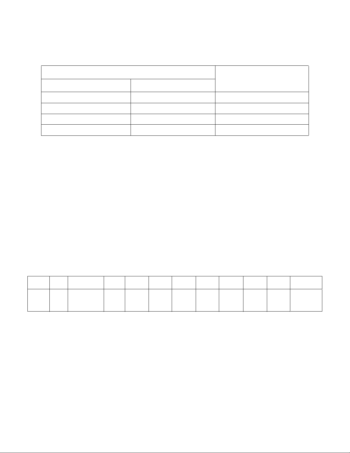
6-Channel Capacitive Touch Sensor with Proximity Detection & Signal Guard
Datasheet
Table 5.29 MTP_TH Bit Decode
MTP_TH[1:0]
0 0 12.5% (default)
0125%
1 0 37.5%
1 1 100%
Bit 1 - COMP_PTRN - Determines whether the MTP detection circuitry will use the Multiple Touch
Pattern register as a specific pattern of sensor inputs or as an absolute number of sensor inputs.
‘0’ (default) - The MTP detection circuitry will use the Multiple Touch Pattern register bit settings as
an absolute minimum number of sensor inputs that must be above the threshold or have Noise
Flag Status bits set. The number will be equal to the number of bits set in the register.
‘1’ - The MTP detection circuitry will use pattern recognition. Each bit set in the Multiple Touch
Pattern register indicates a specific sensor input that must have a delta count greater than the MTP
threshold or have a Noise Flag Status bit set. If the criteria are met, the MTP status bit will be set.
THRESHOLD DIVIDE SETTING10
Bit 0 - MTP_ALERT - Enables an interrupt if an MTP event occurs. In either condition, the MTP status
bit will be set.
‘0’ (default) - If an MTP event occurs, the ALERT# pin is not asserted.
‘1’ - If an MTP event occurs, the ALERT# pin will be asserted.
5.17 Multiple To uch Pattern Register
Table 5.30 Multiple Touch Pattern Register
ADDR R/W REGISTER B7 B6 B5 B4 B3 B2 B1 B0 DEFAULT
2Dh R/W
Multiple
Touch
--
Pattern
The Multiple Touch Pattern register acts as a pattern to identify an expected sensor input profile for
diagnostics or other significant events. There are two methods for how the Multiple Touch Pattern
register is used: as specific sensor inputs or number of sensor input that must exceed the MTP
threshold or have Noise Flag Status bits set. Which method is used is based on the COMP_PTRN bit
(see Section 5.16). The methods are described below.
1. Specific Sensor Inputs: If, during a single sensing cycle, the specific sensor inputs above the MTP
threshold or with Noise Flag Status bits set match those bits set in the Multiple Touch Pattern
register, an MTP event is flagged.
CS6_
PTRN
CS5_
PTRN
CS4_
PTRN
CS3_
PTRN
CS2_
PTRN
CS1_
PTRN
3Fh
2. Number of Sensor Inputs: If, during a single sensing cycle, the number of sensor inputs with a delta
count above the MTP threshold or with Noise Flag Status bits set is equal to or greater than the
number of pattern bits set, an MTP event is flagged.
2013 Microchip Technology Inc. DS01569A-page 47
Page 48

6-Channel Capacitive Touch Sensor with Proximity Detection & Signal Guard
For all bits in this register:
‘0’ - The specified sensor input is not considered a part of the pattern.
‘1’ - The specified sensor input is considered a part of the pattern, or the absolute number of sensor
inputs that must have a delta count greater than the MTP threshold or have the Noise Flag Status
bit set is increased by 1.
Bit 5 - CS6_PTRN - Determines whether CS6 is considered as part of the Multiple Touch Pattern.
Bit 4 - CS5_PTRN - Determines whether CS5 is considered as part of the Multiple Touch Pattern.
Bit 3 - CS4_PTRN - Determines whether CS4 is considered as part of the Multiple Touch Pattern.
Bit 2 - CS3_PTRN - Determines whether CS3 is considered as part of the Multiple Touch Pattern.
Bit 1 - CS2_PTRN - Determines whether CS2 is considered as part of the Multiple Touch Pattern.
Bit 0 - CS1_PTRN - Determines whether CS1 is considered as part of the Multiple Touch Pattern.
5.18 Base Count Out of Limit Register
Table 5.31 Base Count Out of Limit Register
Datasheet
ADDRR/WREGISTERB7B6B5B4B3B2B1B0
2Eh R
Base Count
Out of Limit
--
OUT_
BC_
6
BC_
OUT_
5
BC_
OUT_
4
BC_
OUT_
3
BC_
OUT_
2
BC_
OUT_
1
The Base Count Out of Limit Register indicates which sensor inputs have base counts out of limit (see
Section 4.4, "Sensor Input Calibration"). When these bits are set, the BC_OUT bit is set (see Section
5.2, "Status Registers").
For all bits in this register:
‘0’ - The base count for the specified sensor input is in the ope rating range.
‘1’ - The base count of the specified sensor input is not in the operating range.
Bit 5 - BC_OUT_6 - Indicates whether CS6 has a base count out of limit.
Bit 4 - BC_OUT_5 - Indicates whether CS6 has a base count out of limit.
Bit 3 - BC_OUT_4 - Indicates whether CS6 has a base count out of limit.
Bit 2 - BC_OUT_3 - Indicates whether CS3 has a base count out of limit.
Bit 1 - BC_OUT_2 - Indicates whether CS2 has a base count out of limit.
Bit 0 - BC_OUT_1 - Indicates whether CS1 has a base count out of limit.
5.19 Recalibration Configuration Register
DEFAULT
00h
Ta ble 5.32 Recalibration Configuration Registers
ADDR R/W REGISTER B7 B6 B5 B4 B3 B2 B1 B0 DEFAULT
2Fh R/W
DS01569A-page 48 2013 Microchip Technology Inc.
Recalibration
Configuration
BUT_
LD_TH
NO_CLR
_INTD
NO_CLR
_NEG
NEG_DELTA_
CNT[1:0]
CAL_CFG[2:0] 8Ah
Page 49

6-Channel Capacitive Touch Sensor with Proximity Detection & Signal Guard
Datasheet
The Recalibration Configuration register con trols some recalibration routine settings (see Sectio n 4.4,
"Sensor Input Calibration") as well as advanced controls to program the Sensor Input Threshold
register settings.
Bit 7 - BUT_LD_TH - Enables setting all Sensor Input Threshold registers by writing to the Sensor
Input 1 Threshold register.
‘0’ - Each Sensor Input X Threshold register is updated individually.
‘1’ (default) - Writing the Sensor Input 1 Threshold register will automatically over write the Sensor
Input Threshold registers for all sensor inputs (Sensor Input Threshold 1 through Sen sor Input
Threshold 6). The individual Sensor Input X Threshold registers (Sensor Input 2 T hreshold through
Sensor Input 6 Threshold) can be individually updated at any time.
Bit 6 - NO_CLR_INTD - Controls whether the accumulation of intermediate data is cleared if the noise
status bit is set.
‘0’ (default) - The accumulation of intermediate data is cleared if the noise status bit is set.
‘1’ - The accumulation of intermediate data is not cleared if the noise status bit is set.
APPLICATION NOTE: Bits 5 and 6 should both be set to the same value. Either both should be set to ‘ 0’ or both
should be set to ‘1’.
Bit 5 - NO_CLR_NEG - Controls whether the consecutive negative delta counts counter is cleared if
the noise status bit is set.
‘0’ (default) - The consecutive negative delta counts counter is cleared if the noise status bit is set.
‘1’ - The consecutive negative delta counts counter is not cleared if the noise status bit is set.
Bits 4 - 3 - NEG_DELTA_CNT[1:0] - Determines the number of negative delta counts necessary to
trigger a digital recalibration (see Section 4.4.2, "Negative Delta Count Recalibration"), as shown in
Table 5.33.
Table 5.33 NEG_DELTA_CNT Bit Decode
NEG_DELTA_CNT[1:0]
NUMBER OF CONSECUTIVE NEGATIVE DELTA
COUNT VALUES10
00 8
0 1 16 (default)
10 32
1 1 None (disabled)
Bits 2 - 0 - CAL_CFG[2:0] - Determines the update time and number of samples of the automatic
recalibration routine (see Section 4.4.1, "Automatic Recalibration"). The settings apply to all sensor
inputs universally (though individual sensor inputs can be configured to support recalibration - see
Section 5.11).
2013 Microchip Technology Inc. DS01569A-page 49
Page 50

6-Channel Capacitive Touch Sensor with Proximity Detection & Signal Guard
Datasheet
Table 5.34 CAL_CFG Bit Decode
CAL_CFG[2:0]
RECALIBRATION
SAMPLES (SEE
0 0 0 16 16
001 32 32
0 1 0 64 64 (default)
0 1 1 128 128
100 256 256
1 0 1 256 1024
1 1 0 256 2048
1 1 1 256 4096
Note 5.1 Recalibration Samples refers to the number of samples that are measured and averaged
before the Base Count is updated however does not control the base count u pda te peri od.
Note 5.2 Update Time refers to the amount of time (in sensing cycle periods) that elapses before
the Base Count is updated. The time will depend upon the number of channels enabled,
the averaging setting, and the programmed sensing cycle time.
5.20 Sensor Input Threshold Registers
Note 5.1)
UPDATE TIME (SEE
Note 5.2)210
Table 5.35 Sensor Input Threshold Registers
ADDR R/W REGISTER B7 B6 B5 B4 B3 B2 B1 B0 DEFAULT
30h R/W
31h R/W
32h R/W
33h R/W
34h R/W
35h R/W
Sensor Input 1
Threshold
Sensor Input 2
Threshold
Sensor Input 3
Threshold
Sensor Input 4
Threshold
Sensor Input 5
Threshold
Sensor Input 6
Threshold
-6432168421 40h
-6432168421 40h
-6432168421 40h
-6432168421 40h
-6432168421 40h
-6432168421 40h
The Sensor Input Threshold registers store the delta threshold that is used to determine if a touch has
been detected. When a touch occurs, the input signal of the corresponding sensor pad chang es due
to the capacitance associated with a touch. If the sensor input change excee ds the threshold settings,
a touch is detected.
DS01569A-page 50 2013 Microchip Technology Inc.
Page 51
6-Channel Capacitive Touch Sensor with Proximity Detection & Signal Guard
Datasheet
When the BUT_LD_TH bit is set (see Section 5.19 - bit 7), writi ng data to the Sen sor Input 1 Threshold
register will update all of the Sensor Input Threshold registers (31h - 35h inclusive).
5.21 Sensor Input Noise Threshold Register
Table 5.36 Sensor Inpu t Noise Threshold Register
ADDR R/W REGISTER B7 B6 B5 B4 B3 B2 B1 B0 DEFAULT
38h R/W
Sensor Input
Noise Threshold
------
CS_BN_TH
[1:0]
01h
The Sensor Input Noise Threshold register controls the value of a secondary internal threshold to
detect noise and improve the automatic recalibration routine. If a capacitive touch sensor input exceeds
the Sensor Input Noise Threshold but does not exceed the sensor input threshold, it is determined to
be caused by a noise spike. That sample is not used by the automatic recalibration routine. This
feature can be disabled by setting the DIS_DIG_NOISE bit.
Bits 1-0 - CS1_BN_TH[1:0] - Controls the noise threshold for all capacitive touch sensor inputs, as
shown in Table 5.37. The threshold is proportion al to the threshold setting.
Table 5.37 CSx_BN_TH Bit Decode
CS_BN_TH[1:0]
PERCENT THRESHOLD SETTING10
0025%
0 1 37.5% (default)
1050%
1 1 62.5%
5.22 Standby Channel Register
T able 5.38 Standby Channel Register
ADDR R/W REGISTER B7 B6 B5 B4 B3 B2 B1 B0 DEFAULT
40h R/W
Standby
Channel
--
The Standby Channel register controls which (if any) capacitive touch sensor inputs are enabled in
Standby (see Section 4.3.1.2, "Standby State Sensing Settings").
For all bits in this register:
‘0’ (default) - The specified channel will not be monitored in Standby.
‘1’ - The specified channel will be monitored in Standby. It will use the standby threshold setting,
and the standby averaging and sensitivity settings.
2013 Microchip Technology Inc. DS01569A-page 51
CS6_
STBY
CS5_
STBY
CS4_
STBY
CS3_
STBY
CS2_
STBY
CS1_
STBY
00h
Page 52
6-Channel Capacitive Touch Sensor with Proximity Detection & Signal Guard
Datasheet
Bit 5 - CS6_STBY - Controls whether the CS6 channel is enabled in Standby.
Bit 4 - CS5_STBY - Controls whether the CS5 channel is enabled in Standby.
Bit 3 - CS4_STBY - Controls whether the CS4 channel is enabled in Standby.
Bit 2 - CS3_STBY - Controls whether the CS3 channel is enabled in Standby.
Bit 1 - CS2_STBY - Controls whether the CS2 channel is enabled in Standby.
Bit 0 - CS1_STBY - Controls whether the CS1 channel is enabled in Standby.
5.23 Standby Configuration Register
Table 5.39 Standby Configuration Register
ADDR R/W REGISTER B7 B6 B5 B4 B3 B2 B1 B0 DEFAULT
41h R/W
Standby
Configuration
AVG_
SUM
STBY_AVG[2:0]
STBY_SAMP_
TIME[1:0]
STBY_CY_TIME
[1:0]
The Standby Configuration register controls averaging and sensing cycle time for sensor inputs
enabled in Standby. This register allows the user to change averaging and sample time s on a limited
number of sensor inputs in Standby and still maintain normal functionality in the Active state.
Bit 7 - AVG_SUM - Determines whether the sensor inputs enabled in Standby will average the
programmed number of samples or whether they will accumulate for the programmed number of
samples.
‘0’ - (default) - The Standby enabled sensor input delta count values will be based on the average
of the programmed number of samples when compared against the threshold.
‘1’ - The Standby enabled sensor input delta count values will be based on the summation of the
programmed number of samples when compared against the threshold. Caution should be used
with this setting as a touch may overflow the delta count registers and may result in false readings.
Bits 6 - 4 - STBY_AVG[2:0] - Determines the number of samples that are taken for all Standby enabled
channels during the sensing cycle as shown in Table 5.40. All samples are taken consecutively on the
same channel before the next channel is sampled and the result is averaged over the number of
samples measured before updating the measured results.
Table 5.40 STBY_AVG Bit Decode
STBY_AVG[2:0]
NUMBER OF SAMPLES TAKEN
PER MEASUREMENT210
39h
000 1
001 2
010 4
0 1 1 8 (default)
100 16
101 32
DS01569A-page 52 2013 Microchip Technology Inc.
Page 53

6-Channel Capacitive Touch Sensor with Proximity Detection & Signal Guard
Datasheet
Table 5.40 STBY_AVG Bit Decode (continued)
STBY_AVG[2:0]
110 64
1 1 1 128
Bit 3 - 2 - STBY_SAMP_TIME[1:0] - Determines the time to take a single sample for sensor inputs
enabled in Standby as shown in Table 5.41.
Table 5.41 STBY_SAMP_TIME Bit Decode
STBY_SAMP_TIME[1:0]
0 0 320us
0 1 640us
NUMBER OF SAMPLES TAKEN
PER MEASUREMENT210
SAMPLING TIME10
1 0 1.28ms (default)
1 1 2.56ms
Bits 1 - 0 - STBY_CY_TIME[2:0] - Determines the desired sensing cycle time for sensor inputs enabled
during Standby, as shown in Table 5.42. This control is also used to determine p rogrammed cycle time
in the Combo state (see Section 4.3.1.3, "Combo State Sensing Settings"). All enabled channels are
sampled at the beginning of the sensing cycle. If additional time is remaining, the device is placed into
a lower power state for the remainder of the sensing cycle.
Table 5.42 STBY_CY_TIME Bit Decode
STBY_CY_TIME[1:0]
PROGRAMMED SENSING CYCLE
TIME10
00 35ms
0 1 70ms (default)
1 0 105ms
1 1 140ms
APPLICATION NOTE: The programmed sensing cycle time (STDBY_CY_TIME[1:0] is only maintained if the actual
time to take the samples is less than the p rogrammed cycle time. The STBY_AVG[2:0] bits
will take priority, so the sensing cycle time will be extended as necessary to accommodate
the number of samples to be measured.
2013 Microchip Technology Inc. DS01569A-page 53
Page 54
6-Channel Capacitive Touch Sensor with Proximity Detection & Signal Guard
Datasheet
5.24 Standby Sensitivity Register
Table 5.43 Standby Sensitivity Register
ADDRR/WREGISTER B7 B6 B5B4B3B2B1B0DEFAULT
42h R/W
APPLICATION NOTE: A value of 128x is the most sensitive setting available. At the most sensitivity settings, the
Standby
Sensitivity
The Standby Sensitivity register controls the sensitivity for sensor inputs enabled in Standby.
Bits 2 - 0 - STBY_SENSE[2:0] - Controls the sensitivity for sensor inputs that are enabled in Standby.
The sensitivity settings act to scale the relative delta count value higher or lower based on the system
parameters. A setting of 000b is the most sensitive while a setting of 111b i s the least sensitive. At the
more sensitive settings, touches are detected for a smaller delta capacitance corresponding to a
“lighter” touch. These settings are more sensitive to noise, however, and a noisy environment may flag
more false touches than higher sensitivity levels.
MSB of the Delta Count register represents 64 out of ~25,000 which co rresponds to a touch
of approximately 0.25% of the base capacitance (or a
capacitance). Conversely a value of 1x is the least sensitive setting available. At these
settings, the MSB of the Delta Count register corresponds to a delta count of 8192 counts
out of ~25,000 which corresponds to a touch of approximately 33% of the base capacitance
ΔC of 3.33pF from a 10pF base capacitance).
(or a
- - - - - STBY_SENSE[2:0] 02h
ΔC of 25fF from a 10pF base
Table 5.44 STBY_SENSE Bit Decode
STBY_SENSE[2:0]
SENSITIVITY MULTIPLIER210
0 0 0 128x (most sensitive)
001 64x
0 1 0 32x (default)
011 16x
100 8x
101 4x
110 2x
1 1 1 1x - (least sensitive)
5.25 Standby Threshold Register
Table 5.45 Standby Threshold Register
ADDR R/W REGISTER B7 B6 B5 B4 B3 B2 B1 B0 DEFAULT
43h R/W
DS01569A-page 54 2013 Microchip Technology Inc.
Standby
Threshold
-6432168421 40h
Page 55

6-Channel Capacitive Touch Sensor with Proximity Detection & Signal Guard
Datasheet
The Standby Threshold register stores the delta threshold that is used to determine if a touch has been
detected. When a touch occurs, the input signal of the corresponding sensor pad changes due to the
capacitance associated with a touch. If the sensor input change exceeds the threshold settings, a
touch is detected.
5.26 Sensor Input Base Count Registers
Table 5.46 Sensor Inp ut Base Count Registers
ADDR R/W REGISTER B7 B6 B5 B4 B3 B2 B1 B0 DEFAULT
50h R
51h R
52h R
53h R
54h R
55h R
Sensor Input 1
Base Count
Sensor Input 2
Base Count
Sensor Input 3
Base Count
Sensor Input 4
Base Count
Sensor Input 5
Base Count
Sensor Input 6
Base Count
The Sensor Input Base Count registers store the calibrated “not touched” input value from the
capacitive touch sensor inputs. These registers are periodically updated by the calibration and
recalibration routines.
The routine uses an internal adder to add the current count value for each readin g to the sum of the
previous readings until sample size has been reac hed. At this point, the upper 16 bits are taken and
used as the Sensor Input Base Count. The internal adder is then reset and the reca libration routine
continues.
The data presented is determined by the BASE_SHIFT[3:0] bits (see Section 5.5).
128 64 32 16 8 4 2 1 C8h
128 64 32 16 8 4 2 1 C8h
128 64 32 16 8 4 2 1 C8h
128 64 32 16 8 4 2 1 C8h
128 64 32 16 8 4 2 1 C8h
128 64 32 16 8 4 2 1 C8h
5.27 Power Button Register
Table 5.47 Power Button Register
ADDR R/W REGISTER B7 B6 B5 B4 B3 B2 B1 B0 DEFAULT
60h R/W Power Button - - - - - PWR_BTN[2:0] 00h
The Power Button Register indicates the sensor input that has been designated as the p ower button
(see Section 4.6, "Power Button").
Bits 2 - 0 - PWR_BTN[2:0] - When the power button feature is enabled, this control indicates the
sensor input to be used as the power button. The decode is shown in Table 5.48.
2013 Microchip Technology Inc. DS01569A-page 55
Page 56

6-Channel Capacitive Touch Sensor with Proximity Detection & Signal Guard
Table 5.48 PWR_BTN Bit Decode
PWR_BTN[3:0]
SENSOR INPUT DESIGNATED AS POWER BUTTON201
000 CS1
001 CS2
010 CS3
011 CS4
100 CS5
101 CS6
5.28 Power Button Configuration Register
Datasheet
Table 5.49 Power Button Configuration Register
ADDR R/W REGISTER B7 B6 B5 B4 B3 B2 B1 B0 DEFAULT
STBY_
-
PWR_
EN
STBY_PWR_
TIME [1:0]
PWR_
-
EN
PWR_TIME [1:0] 22h
61h R/W
Power Button
Configuration
The Power Button Configuration Register controls the length of time that the designate d power button
must indicate a touch before an interrupt is generated and the power status indicator is set (see
Section 4.6, "Power Button").
Bit 6 - STBY_PWR_EN - Enables the power button feature in the Standby state.
‘0’ (default) - The Standby power button circuitry is disabled.
‘1’ - The Standby power button circuitry is enabled.
Bits 5 - 4 - STBY_PWR_TIME[1:0] - Determines the overall time, as shown in Table 5.50, that the
power button must be held in the Standby state, in order for an interrupt to be generated and the PWR
bit to be set.
Bit 2 - PWR_EN - Enables the power button feature in the Acti ve state.
‘0’ (default) - The power button circuitry is disabled in the Active state.
‘1’ -The power button circuitry is enabled in the Active state.
Bits 1 - 0 - PWR_TIME[1:0] - Determines the overall time, as shown in Table 5.50, that the power
button must be held in the Active state, in order for an interrupt to be generated and the PWR bit to
be set.
DS01569A-page 56 2013 Microchip Technology Inc.
Page 57
6-Channel Capacitive Touch Sensor with Proximity Detection & Signal Guard
Datasheet
Table 5.50 Power Button Time Bits Decode
PWR_TIME[1:0] / STBY_PWR_TIME[1:0]
POWER BUTTON TOUCH HOLD TIME10
0 0 280ms
0 1 560ms
1 0 1.12 sec (default)
1 1 2.24 sec
5.29 Sensor Input Calibration Registers
Table 5.51 Sensor Input Calibration Registers
ADDR REGISTER R/W B7 B6 B5 B4 B3 B2 B1 B0 DEFAULT
B1h
B2h
B3h
B4h
B5h
B6h
B9h
BAh
Sensor Input 1
Calibration
Sensor Input 2
Calibration
Sensor Input 3
Calibration
Sensor Input 4
Calibration
Sensor Input 5
Calibration
Sensor Input 6
Calibration
Sensor Input
Calibration
LSB 1
Sensor Input
Calibration
LSB 2
R CAL1_9 CAL1_8 CAL1_7 CAL1_6 CAL1_5 CAL1_4 CAL1_3 CAL1_2 00h
R CAL2_9 CAL2_8 CAL2_7 CAL2_6 CAL2_5 CAL2_4 CAL2_3 CAL2_2 00h
R CAL3_9 CAL3_8 CAL3_7 CAL3_6 CAL3_5 CAL3_4 CAL3_3 CAL3_2 00h
R CAL4_9 CAL4_8 CAL4_7 CAL4_6 CAL4_5 CAL4_4 CAL4_3 CAL4_2 00h
R CAL5_9 CAL5_8 CAL5_7 CAL5_6 CAL5_5 CAL5_4 CAL5_3 CAL5_2 00h
R CAL6_9 CAL6_8 CAL6_7 CAL6_6 CAL6_5 CAL6_4 CAL6_3 CAL6_2 00h
R CAL4_1 CAL4_0 CAL3_1 CAL3_0 CAL2_1 CAL2_0 CAL1_1 CAL1_0 00h
R - - - - CAL6_1 CAL6_0 CAL5_1 CAL5_0 00h
The Sensor Input Calibration registers hold the 10-bit value that represents the last calibration value.
The value represents the capacitance applied to the internal sensing circuits to balance the
capacitance of the sensor input pad. Minimum (000h) and maximum (3FFh) values indicate analog
calibration failure (see Section 4.4, "Sensor Input Calibration").
2013 Microchip Technology Inc. DS01569A-page 57
Page 58
6-Channel Capacitive Touch Sensor with Proximity Detection & Signal Guard
5.30 Calibration Sensitivity Configuration Registers
Table 5.52 Calibration Sensitivity Configuration Registers
Datasheet
ADDR REGISTER R/W B7 B6 B5 B4 B3 B2 B1 B0
80h
81h
Calibration
Sensitivity
Config 1
Calibration
Sensitivity
Config 2
CALSENx[1:0] - Controls the gain used by the calibration routine to enable sensor inputs to be more
sensitive for proximity detection. Gain is based on capacitance touch pad capacitance ranges, as
shown in Table 5.53. Since each sensor input can have a different pad capacitance, each sensor input
has a control.
CALSENX[1:0]
0 0 1 5-50pF (default)
012 0-25pF
1 0 4 0-12.5pF
R/W CALSEN4[1:0] CALSEN3[1:0] CALSEN2[1:0] CALSEN1[1:0] 00h
R/W----CALSEN6[1:0]CALSEN5[1:0]00h
Table 5.53 CALSENX Bit Decode
GAIN
CAPACITIVE TOUCH PAD
CAPACITANCE RANGE10
DEFAULT
5.31 Product ID Register
Table 5.54 Product ID Register
ADDR R/W REGISTER B7 B6 B5 B4 B3 B2 B1 B0 DEFAULT
FDh R
Product ID
CAP1296-1
The Product ID register stores a unique 8-bit value that identifies the device.
01101001 69h
5.32 Manufacturer ID Register
Table 5.55 Vendor ID Register
ADDR R/W REGISTER B7 B6 B5 B4 B3 B2 B1 B0 DEFAULT
FEh RManufacturer ID01011101 5Dh
The Vendor ID register stores an 8-bit value that represents MCHP.
DS01569A-page 58 2013 Microchip Technology Inc.
Page 59

6-Channel Capacitive Touch Sensor with Proximity Detection & Signal Guard
Datasheet
5.33 Revision Register
Table 5.56 Revision Register
ADDR R/W REGISTER B7 B6 B5 B4 B3 B2 B1 B0 DEFAULT
FFhR Revision 00000000 00h
The Revision register stores an 8-bit value that represen ts the part revision.
2013 Microchip Technology Inc. DS01569A-page 59
Page 60

6-Channel Capacitive Touch Sensor with Proximity Detection & Signal Guard
Chapter 6 Package Information
6.1 CAP1296 Package Drawings
Datasheet
Figure 6.1 CAP1296 Package Drawing - 10-Pin DFN 3mm x 3mm
DS01569A-page 60 2013 Microchip Technology Inc.
Page 61
6-Channel Capacitive Touch Sensor with Proximity Detection & Signal Guard
Datasheet
Figure 6.2 CAP1296 Package Dimensio ns - 10-Pin DFN 3mm x 3mm
Figure 6.3 CAP1296 PCB Land Pattern and Stencil - 10-Pin DFN 3mm x 3mm
2013 Microchip Technology Inc. DS01569A-page 61
Page 62

6-Channel Capacitive Touch Sensor with Proximity Detection & Signal Guard
Datasheet
Figure 6.4 CAP1296 PCB Detail A - 10-Pin DFN 3mm x 3mm
DS01569A-page 62 2013 Microchip Technology Inc.
Page 63

6-Channel Capacitive Touch Sensor with Proximity Detection & Signal Guard
Datasheet
Figure 6.5 CAP1296 PCB Detail B - 10-Pin DFN 3mm x 3mm
Figure 6.6 CAP1296 Land Dimensio ns - 10-Pin DFN 3mm x 3mm
2013 Microchip Technology Inc. DS01569A-page 63
Page 64
6.2 Package Marking
BOTTOM
LINE 1: Device code, first 2 of last 6
digits of lot number
LINE 2: Last 4 digits of lot number
TOP
e4
PIN 1
BOTTOM MARKING IS NOT ALLOWED
2 9 L L
L L L L
Figure 6.7 CAP1296-1 Package Marking
6-Channel Capacitive Touch Sensor with Proximity Detection & Signal Guard
Datasheet
DS01569A-page 64 2013 Microchip Technology Inc.
Page 65

6-Channel Capacitive Touch Sensor with Proximity Detection & Signal Guard
Datasheet
Appendix A Device Delta
A.1 Delta from CAP1106-1 to CAP1296-1
The CAP1296 is pin- and register-compatible with the CAP1106, with the exception of the ALT_POL
bit.
1. Revision ID set to 00h.
2. Added Power Button feature (see Section 4.6, "Power Button").
3. Added ACAL_FAIL bit to flag analog calibration failures (see Section 5.2, "Status Registers") and
ACAL_FAIL_INT bit to control analog calibration failure interrupts (see Section 5.6, "Configuration
Registers").
4. Added BC_OUT bit to flag calibration failures regarding base counts out of limit (see Se ction 5.2,
"Status Registers") and BC_OUT_RECAL and BC_OUT_INT bit to control base count out of limit
behavior and interrupts (see Section 5.6, "Configuration Registers"). Added Base Count Out of
Limit Register to indicate which sensor inputs have base counts outside the operating range (see
Section 5.18, "Base Count Out of Limit Register").
5. New Combo state has been added which allows some sensors programmed to use the Acti ve state
settings and other sensors programmed to use the Standby state settings to function at the same
time (see Section 4.3.1.3, "Combo State Sensing Settings").
6. Added an option for a signal guard that is overloaded with the CS2 pin. This signal guard is
configured to power a ground shield for improved sign al in certain applications (see Section 4.5.1,
"Signal Guard").
7. Increased supply voltage range for 5V operation.
8. Increased operating temperature range from 0°C - 85°C to -40°C to 125°C.
9. Removed ALERT
10. Register additions are shown in Table A.1, "Register Delta".
ADDRESS REGISTER DELTA DELTA DEFAULT
00h
Page 30
02h
Page 32
26h
Page 42
29h
Page 45
2Eh
Page 48
Added bits - Main
Added bits - General
Renamed Calibration
Activate and Status
Register and added
New - Signal Guard
New - Base Count Out
of Limit Register
pin configuration (ALT_POL bit).
Table A.1 Register Delta
Added C_GAIN[1:0] and COMBO bits.
Control Register
Added bit 4 PWR for new Power Button
Status Register
functionality
Enable Register
indicate analog calibration failure. Added
In addition to forcing a calibration, the
Changed function of GAIN[1:0] bits if
COMBO bit is set.
feature. Added bit 5 ACAL_FAIL to
bit 6 BC_OUT.
register also indicates the status of
calibration for each sensor input.
new register for Signal Guard feature 00h
new register for calibration status 00h
00h
00h
00h
2013 Microchip Technology Inc. DS01569A-page 65
Page 66

6-Channel Capacitive Touch Sensor with Proximity Detection & Signal Guard
Datasheet
Table A.1 Register Delta (continued)
ADDRESS REGISTER DELTA DELTA DEFAULT
44h
Page 36
60h
Page 55
61h
Page 56
80h
Page 58
81h
Page 58
FDh
Page 58
FFh
Page 59
Added and removed
bits - Configuration 2
Register
New - Power Button
Register
New - Power Button
Configuration Register
Added - Calibration
Sensitivity Config 1
Added - Calibration
Sensitivity Config 2
Added bit 1 ACAL_FAIL_INT. Added bit 4
BC_OUT_INT. Changed bit 6 from
ALT_POL to BC_OUT_RECAL.
new register for Power Button feature 00h
new register for configuring the Power
Button feature
new register for proximity 00h
new register for proximity 00h
40h
00h
Changed - Product ID New product ID for CAP1296-1 69h
Changed - Revision
Register
Revision changed. 00h
DS01569A-page 66 2013 Microchip Technology Inc.
Page 67

6-Channel Capacitive Touch Sensor with Proximity Detection & Signal Guard
Datasheet
Revision History
Table 6.1 Revision History
REVISION LEVEL AND
DATE SECTION/FIGURE/ENTRY CORRECTION
CAP1296 Revision A replaces the previous SMSC version Re vision 1.0
2013 Microchip Technology Inc. DS01569A-page 67
Page 68

6-Channel Capacitive Touch Sensor with Proximity Detection & Signal Guard
YSTEM
CERTIFIED BY DNV
== ISO/TS 16949 ==
Datasheet
Note the following details of the code protection feature on Microchip devices:
• Microchip products meet the specification contained in their particular Microchip Data Sheet.
• Microchip believes that its family of products is one of the most secure families of its kind on the market today, when used in the
intended manner and under normal conditions.
• There are dishonest and possibly illegal methods used to breach the code protection feature. All of these methods, to our
knowledge, require using the Microchip products in a manner outside the operating specifications contained in Microchip’s Data
Sheets. Most likely, the person doing so is engaged in theft of intellectual property.
• Microchip is willing to work with the customer who is concerned about the integrity of their code.
• Neither Microchip nor any other semiconductor manufacturer can guarantee the security of their code. Code protection does not
mean that we are guaranteeing the product as “unbreakable.”
Code protection is constantly evolving. We at Microchip are committed to continuously improving the code protection features of our
products. Attempts to break Microchip’s code protection feature may be a violation of the Digital Millennium Copyright Act. If such acts
allow unauthorized access to your software or other copyrighted work, you may have a right to sue for relief under that Act.
Information contained in this publication regarding device applications and the like is provided only for your convenience and may be
superseded by updates. It is your responsibility to ensure that your application meet s with y our specifications. MICROCHIP MA KES NO
REPRESENTATIONS OR WARRANTIES OF ANY KIND WHETHER EXPRESS OR IMPLIED, WRITTEN OR ORAL, STA TUT OR Y OR
OTHERWISE, RELATED TO THE INFORMATION, INCLUDING BUT NOT LIMITED TO ITS CONDITION, QUALITY , PERFORMANCE,
MERCHANTABILITY OR FITNESS FOR PURPOSE. Microchip disclaims all liability arising from this information and its use. Use of
Microchip devices in life support and/or safety applications is entirely at the buyer’s risk, and the buyer agrees to defend, indemnify and
hold harmless Microchip from any and all damages, claims, suits, or expenses resulting from such use. No licenses are conveyed, implicitly or otherwise, under any Microchip intellectual prope rty rights.
Trademarks
The Microchip name and logo, the Microchip logo, dsPIC, FlashFlex, K
logo, rfPIC, SST , SST Logo, SuperFlash and UNI/O are registered trademarks of Microchip T echnology Incorporated in the U.S.A. and
other countries.
FilterLab, Hampshire, HI-TECH C, Linear Active Thermistor, MTP, SEEVAL and The Embedded Control Solutions Company are
registered trademarks of Microchip Technology Incorporated in the U.S.A.
Silicon Storage Technology is a reg istered trademark of Microchip Technology Inc. in other countries.
Analog-for-the-Digital Age, Application Maestro, BodyCom, chipKIT, chipKIT logo, CodeGuard, dsPICDEM, dsPICDEM.net,
dsPICworks, dsSPEAK, ECAN, ECONOMONITOR, FanSense, HI-TIDE, In-Circuit Serial Programming, ICSP, Mindi, MiWi, MPASM,
MPF , MPLAB Certified logo, MPLIB, MPLINK, mTouch, Omniscient Code Generation, PICC, PICC-18, PICDEM, PICDEM.net, PICkit,
PICtail, REAL ICE, rfLAB, Select Mode, SQI, Serial Quad I/O, Total Endurance, TSHARC, UniWinDriver, WiperLock, ZENA and ZScale are trademarks of Microchip Technology Incorporated in the U.S.A. and other countries.
SQTP is a service mark of Microchip Technology Incorporated in the U.S.A.
GestIC and ULPP are registered trademarks of Microchip Technology Germany II GmbH & Co. KG, a subsidiary of Microchip
Technology Inc., in other countries.
A more complete list of registered trademarks and common law trademarks owned by Standard Microsystems Corporation (“SMSC”)
is available at: www.smsc.com. The absence of a trademark (name, logo, etc.) from the list does not constitute a waiver of any
intellectual property rights that SMSC has established in any of its trademarks.
All other trademarks mentioned herein are property of their respective companies.
© 2013, Microchip Technology Incorporated, Printed in the U.S.A., All Rights Reserved.
ISBN: 9781620774472
EELOQ, KEELOQ logo, MPLAB, PIC, PICmicro, PICSTART, PIC
32
QUALITY MANAGEMENT S
DS01569A-page 68 2013 Microchip Technology Inc.
Microchip received ISO/TS-16949:2009 certification for its worldwide
headquarters, design and wafer fabrication facilities in Chandler and
T empe, Arizona; Gresham, Oregon and design centers in California
and India. The Company’s quality system processes and procedures
are for its PIC
devices, Serial EEPROMs, microperipherals, nonvolatile memory and
analog products. In addition, Microchip’s quality system for the desig n
and manufacture of development systems is ISO 9001:2000 certified.
®
MCUs and dsPIC® DSCs, KEELOQ
®
code hopping
Page 69

Worldwide Sales and Service
AMERICAS
Corporate Office
2355 West Chandler Blvd.
Chandler, AZ 85224-6199
Tel: 480-792-7200
Fax: 480-792-7277
Technical Support:
http://www.microchip.com/
support
Web Address:
www.microchip.com
Atlanta
Duluth, GA
Tel: 678-957-9614
Fax: 678-957-1455
Boston
Westborough, MA
Tel: 774-760-0087
Fax: 774-760-0088
Chicago
Itasca, IL
Tel: 630-285-0071
Fax: 630-285-0075
Cleveland
Independence, OH
Tel: 216-447-0464
Fax: 216-447-0643
Dallas
Addison, TX
Tel: 972-818-7423
Fax: 972-818-2924
Detroit
Farmington Hills, MI
Tel: 248-538-2250
Fax: 248-538-2260
Indianapolis
Noblesville, IN
Tel: 317-773-8323
Fax: 317-773-5453
Los Angeles
Mission Viejo, CA
Tel: 949-462-9523
Fax: 949-462-9608
Santa Clara
Santa Clara, CA
Tel: 408-961-6444
Fax: 408-961-6445
Toronto
Mississauga, Ontario,
Canada
Tel: 905-673-0699
Fax: 905-673-6509
ASIA/PACIFIC
Asia Pacific Office
Suites 3707-14, 37th Floor
Tower 6, The Gateway
Harbour City, Kowloon
Hong Kong
Tel: 852-2401-1200
Fax: 852-2401-3431
Australia - Sydney
Tel: 61-2-9868-6733
Fax: 61-2-9868-6755
China - Beijing
Tel: 86-10-8569-7000
Fax: 86-10-8528-2104
China - Chengdu
Tel: 86-28-8665-5511
Fax: 86-28-8665-7889
China - Chongqing
Tel: 86-23-8980-9588
Fax: 86-23-8980-9500
China - Hangzhou
Tel: 86-571-2819-3187
Fax: 86-571-2819-3189
China - Hong Kong SAR
Tel: 852-2943-5100
Fax: 852-2401-3431
China - Nanjing
Tel: 86-25-8473-2460
Fax: 86-25-8473-2470
China - Qingdao
Tel: 86-532-8502-7355
Fax: 86-532-8502-7205
China - Shanghai
Tel: 86-21-5407-5533
Fax: 86-21-5407-5066
China - Shenyang
Tel: 86-24-2334-2829
Fax: 86-24-2334-2393
China - Shenzhen
Tel: 86-755-8864-2200
Fax: 86-755-8203-1760
China - Wuhan
Tel: 86-27-5980-5300
Fax: 86-27-5980-5118
China - Xian
Tel: 86-29-8833-7252
Fax: 86-29-8833-7256
China - Xiamen
Tel: 86-592-2388138
Fax: 86-592-2388130
China - Zhuhai
Tel: 86-756-3210040
Fax: 86-756-3210049
ASIA/PACIFIC
India - Bangalore
Tel: 91-80-3090-4444
Fax: 91-80-3090-4123
India - New Delhi
Tel: 91-11-4160-8631
Fax: 91-11-4160-8632
India - Pune
Tel: 91-20-3019-1500
Japan - Osaka
Tel: 81-6-6152-7160
Fax: 81-6-6152-9310
Japan - Tokyo
Tel: 81-3-6880- 3770
Fax: 81-3-6880-3771
Korea - Daegu
Tel: 82-53-744-4301
Fax: 82-53-744-4302
Korea - Seoul
Tel: 82-2-554-7200
Fax: 82-2-558-5932 or
82-2-558-5934
Malaysia - Kuala Lumpur
Tel: 60-3-6201-9857
Fax: 60-3-6201-9859
Malaysia - Penang
Tel: 60-4-227-8870
Fax: 60-4-227-4068
Philippines - Manila
Tel: 63-2-634-9065
Fax: 63-2-634-9069
Singapore
Tel: 65-6334-8870
Fax: 65-6334-8850
Taiwan - Hsin Chu
Tel: 886-3-5778-366
Fax: 886-3-5770-955
Taiwan - Kaohsiung
Tel: 886-7-213-7828
Fax: 886-7-330-9305
Taiwan - Taipei
Tel: 886-2-2508-8600
Fax: 886-2-2508-0102
Thailand - Bangkok
Tel: 66-2-694-1351
Fax: 66-2-694-1350
EUROPE
Austria - Wels
Tel: 43-7242-2244-39
Fax: 43-7242-2244-393
Denmark - Copenhagen
Tel: 45-4450-2828
Fax: 45-4485-2829
France - Paris
Tel: 33-1-69-53-63-20
Fax: 33-1-69-30-90-79
Germany - Munich
Tel: 49-89-627-144-0
Fax: 49-89-627-144-44
Italy - Milan
Tel: 39-0331-742611
Fax: 39-0331-466781
Netherlands - Drunen
Tel: 31-416-690399
Fax: 31-416-690340
Spain - Madrid
Tel: 34-91-708-08-90
Fax: 34-91-708-08-91
UK - Wokingham
Tel: 44-118-921-5869
Fax: 44-118-921-5820
08/20/13
DS01569A-page 69 2013 Microchip Technology Inc.
 Loading...