

Page 1

CAM35C44
ADVANCE INFORMATION
Infrared Communications Controller Chip
CameraFR
FEATURES
!"
Mixed Voltage Support
- Supports 3.3V Operation
- Supports Mixed Internal 3.3V
Operation with 3.3V/5V External
Configuration
!"
Intelligent Auto Power Management
- Supports Multiple Power Down
Modes
!"
Serial Port
- High Speed NS16C550A Compatible
UART with 16-Byte Send/Receive
FIFOs
- Programmable Baud Rate Generator
!"
Infrared Port
- Multi-Protocol Infrared Interface
- 128-Byte Data FIFO
- IrDA 1.1 Compliant (up to 4Mbps)
- Consumer IR
- SHARP ASK IR
- Programmed I/O and DMA Options
GENERAL DESCRIPTION
The CAM35C44 with IrDA v1.1 (4Mbps) and
Consumer IR support incorporates SMSC’s
advanced Infrared Communications Controller
(IrCC 2.0), a 16C550A-compatible UART,
Multiple Host Interface options, flexible Address
Decoding and up to five General Purpose I/Os.
!"
!"
- ISA-Style 5 Bit Address and 8 Bit
Data Bus
- IOCHRDY and No Wait State Support
for Fast IR
- Non-ISA 8 Bit Multiplexed
Address/Data Bus
- Programmable Read/Write Interface
- One 8 Bit DMA Channel
- One Programmable IRQ
- Chip Select
- Multihost Interface Support Includes
Hitachi and Mitsubishi
Microcontrollers
!"
- Supports Internal or External Clock
Source
!"
The CAM35C44 also features sophisticated
power control circuitry to support multiple power
down modes, an on-chip 24MHz crystal
oscillator, and
The CAM35C44 is particularly suited for 3.3v
battery-powered systems.
Up to 5 General Purpose I/O Pins
Programmable Multi-Protocol Host Interface
24MHz Crystal Oscillator
48 Pin TQFP Package
12mA
host bus drivers.
Page 2

TABLE OF CONTENTS
FEATURES.............................................................................................................................................. 1
GENERAL DESCRIPTION......................................................................................................................1
ARCHITECTURE.....................................................................................................................................4
PIN CONFIGURATION............................................................................................................................5
DESCRIPTION OF PIN FUNCTIONS......................................................................................................6
UFFER-TYPE SUMMARY
B
........................................................................................................................... 11
CLOCK GENERATOR........................................................................................................................... 12
MULTIHOST CPU INTERFACE............................................................................................................ 13
OST INTERFACE SELECT
H
OST INTERFACE PIN MULTIPLEXING
H
.......................................................................................................................... 14
........................................................................................................... 14
System Data Bus ................................................................................................................................... 14
ISA Address Bus SA0 - SA1..................................................................................................................15
ISA Address Bus SA2 - SA4..................................................................................................................15
ISA nIOR................................................................................................................................................15
ISA nIOW...............................................................................................................................................15
REGISTER ADDRESS MAP..................................................................................................................16
ULTIPLEXED
NON-M
ULTIPLEXED ADDRESSING
M
DDRESSING
(ISA) A
....................................................................................................... 16
........................................................................................................................ 17
CONFIGURATION.................................................................................................................................18
ONFIGURATION ACCESS PORTS
C
ONFIGURATION STATE
C
ONFIGURATION REGISTERS
C
............................................................................................................................. 19
................................................................................................................ 18
...................................................................................................................... 21
INFRARED INTERFACE.......................................................................................................................30
IRDA SIR/FIR ......................................................................................................................................... 30
ASKIR .................................................................................................................................................... 30
ONSUMER
C
ARDWARE INTERFACE
H
IR.......................................................................................................................................... 30
............................................................................................................................. 30
GENERAL PURPOSE I/O ..................................................................................................................... 32
NTRODUCTION
I
ESCRIPTION
D
EGISTERS
R
..........................................................................................................................................32
............................................................................................................................................32
..............................................................................................................................................34
DC ELECTRICAL CHARACTERISTICS............................................................................................... 36
A.C. TIMING .......................................................................................................................................... 38
LOCK AND RESET TIMING
C
EAD CYCLE TIMING (NON-MULTIPLEXED
R
EAD CYCLE TIMING (MULTIPLEXED
R
RITE CYCLE TIMING (NON-MULTIPLEXED
W
RITE CYCLE TIMING (MULTIPLEXED
W
......................................................................................................................... 38
)................................................................................................... 39
)........................................................................................................... 40
)................................................................................................. 41
)......................................................................................................... 42
2
Page 3

EAD/WRITE CYCLE TIMING (MULTIPLEXED
R
INGLE TRANSFER MODE
S
URST TRANSFER MODE
B
DMA T
DMA T
IMING
IMING
)................................................................................................43
....................................................................................................... 44
........................................................................................................ 46
3
Page 4
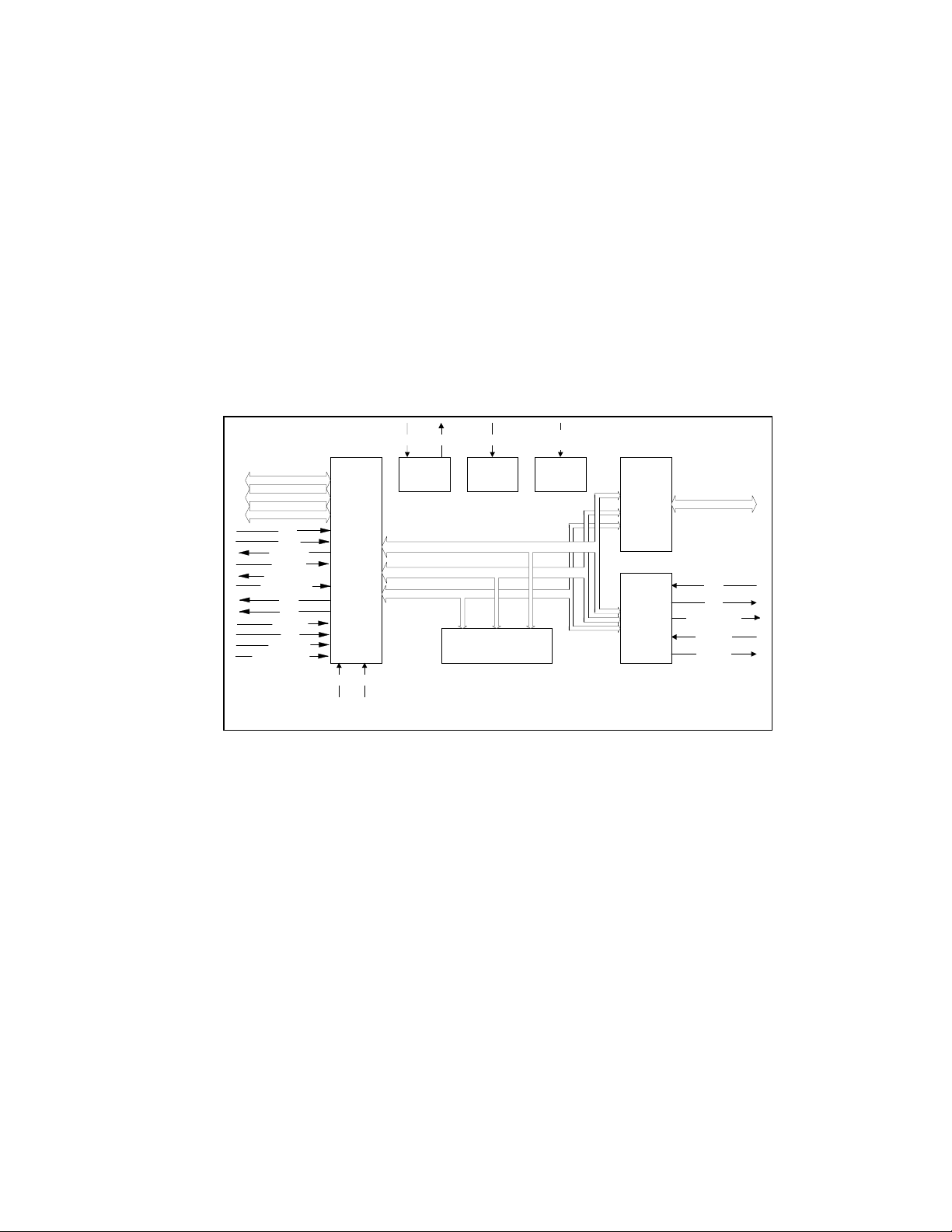
ARCHITECTURE
There are six basic architectural components in
the CAM35C44: the multihost CPU interface, the
IrCC 2.0, a clock generator, configuration
registers, power management, and general
purpose I/O (
FIGURE
The multihost CPU interface is capable of
supporting several bus configurations; including,
a non-multiplexed ISA-style address and data
bus, and a multiplexed address/data bus with
selectable read/write command options. The
multihost CPU interface includes support for
Hitachi and Mitsubishi microcontrollers.
1
).
nIOW/DSTRB
SD[7:0]/AD[7:0]
SA[1:0]/GPIO[4:3]
SA[4:2]/BS[2:0]
nCS
AEN
IOCHRDY
ASTRB
nNOWS
RESET_DRV
IRQ
DRQ
nDACK
TC
nIOR/RW
X1/CLK1 x2 PWRGD
CLOCK
GEN
MULTIHOST
CPU
INTERFACE
HS1 HS0
CONTROL
ADDRESS
CONFIGURATION
FIGURE 1 - CAM35C44 BLOCK DIAGRAM
The IrCC 2.0 is a multi-protocol serial
communications controller that incorporates an
ACE 16C550A UART and a Synchronous
Communications Engine (SCE). Refer to the
SMSC Infrared Communications Controller 2.0
specification for more information.
The clock generator provides connections for a
24MHz crystal or an external clock source. The
24MHz clock directly drives the ACE block. An
internal PLL is used for data rates above
115.2Kbps.
Power management in the CAM35C44 includes
various power down modes and an infrared
wake-up option. The general purpose I/O
interface provides generic I/O programming
capabilities.
VCC[2:1],VSS[3:1],
POWER
MGMT
VIO
POWER
GENERAL
PURPOSE
I/O
GPIO[2:0]
DATA
REGISTERS
IRCC 2.0
IRRX
IRTX
IRMODE/IRRX3
RXD/IRRX
TXD/IRTX
4
Page 5

PIN CONFIGURATION
The CAM35C44 pin numbers are shown in
FIGURE 2. Functional descriptions per pin-
N/C
SA2/BS2
SA1/GP IO4
SA0/GP IO3
PWRG D
48
47
46
45
SA3/BS1
SA4/BS0
TXD/IRTX
IRTX
IRMODE/IRRX3
VIO
nIOR/RnW
nIOW/DSTRB
nNOWS
AEN
nCS
N/C
1
2
3
4
5
6
7
8
9
10
11
12
13
N/C
48 PI N T QFP
14
15
SD0/AD0
SD1/AD1
FIGURE 2 - CAM35C44 PIN CONFIGURATION
44
CAM35C44
16
17
SD2/AD2
SD3/AD3
group are shown in TABLE 1.
Note: The pin numbers in FIGURE 2 are subject
to change.
VSS
ASTRB
VDD
GPIO2
GPIO1
GPIO0
VSS
43
42
41
40
39
38
37
HS1
36
HS0
35
X2
34
X1/CLK1
33
IRRX
18
19
20
21
22
32
RXD/IRRX
31
TC
30
IOCHRDY
29
RESET_DRV
28
VDD
27
nDAC K
26
N/C
25
23
24
SD4/AD4
SD5/AD5
SD6/AD6
SD7/AD7
IRQ
VSS
DRQ
5
Page 6

DESCRIPTION OF PIN FUNCTIONS
TABLE 1 - CAM35C44 PIN FUNCTION DESCRIPTION
NAME
ISA System Data Bus/
Multiplexed
Address/Data Bus
(Non-ISA)
ISA System Address
Bus (SA0 - SA1)/
General Purpose I/O
(GPIO3 - GPIO4)
ISA System Address
Bus (SA2 - SA4)/
Memory Block Selects
(BS0 - BS2)
Chip Select 1 nCS I The active low chip select input is
4
TOTAL
PINS
PROCESSOR/HOST INTERFACE (25)
8 SD[7:0]/AD[7:0] IO12 T his 8 bit bus is used to exchange
2 SA[1:0]/GPIO[4:3] I/IO12 The ISA system address bus is
3 SA[4:2]/BS[2:0] I The ISA system address bus is
SYMBOL
BUFFER
TYPE
DESCRIPTION
data with the host. The bus is bidirectional and can be configured
as either an ISA system data bus
or as a multiplexed address/data
bus (TABLE 3). These pins are in
a high-impedance state when not
in the output mode.
used to determine the I/O address
during read and write cycles.
These two ISA system address
bus pins are general purpose I/O
pins (TABLE 30) when a
multiplexed address/data host
interface type is selected (TABLE
3).
used to determine the I/O address
during read and write cycles.
These three ISA system address
bus pins are memory block select
pins (TABLE 10) when a
multiplexed address/data host
interface type is selected (TABLE
3).
a 32-byte address block decoder
when the ISA host interface type
is selected and a 256-byte page
decoder when a multiplexed
address/data host interface type is
selected (TABLE 3).
6
Page 7

NAME
Address Enable 1 AEN I The active high Address Enable
ISA I/O Channel Ready 1 IOCHRDY OD12 IOCHRDY is pulled low to extend
Multiplex Mode
Address Strobe
No Wait State 1 nNOWS OD12 nNOWS can be enabled to be
ISA Reset Drive 1 RESET_DRV IS The RESET_DRV pin is active
IRQ
TOTAL
PINS
1 ASTRB I ASTRB is used to internally latch
1 IRQ
SYMBOL
BUFFER
TYPE
pin indicates DMA operations on
the host data bus. AEN must be
inactive to access the CAM35C44
registers and active during DMA
operations regardless of the
selected host interface type.
ISA I/O read/write commands.
Only SCE-driven functions in the
IrCC 2.0 can be enabled to use
IOCHRDY.
I/O addresses during read/write
cycles when a multiplexed
address/data host interface type is
selected (TABLE 3).
activated by IrCC 2.0 SCE-driven
functions to indicate that an
access cycle shorter than the
standard ISA I/O cycle can be
executed.
high and is used to reset the
CAM35C44 as described in the
appropriate sections in this
document. The configuration
registers are not affected by this
pin except where noted (TABLE
13). The RESET_DRV pin must
be valid for 500ns minimum.
OD12 The IRQ pin is forced active when
an interrupt is asserted. IRQ goes
inactive as soon as the source of
the interrupt has been cleared.
The active IRQ pin-state is
determined by the IRQ_LEV bit in
CR00 (see page 22).
DESCRIPTION
7
Page 8

NAME
DMA Request 1 DRQ O12 The DRQ pin is forced active by
DMA Acknowledge 1 DACK I The DACK pin is forced active by
Terminal Count 1 TC I TC indicates that a DMA transfer
ISA I/O Read/
Non-ISA Read/Write
Control
ISA I/O Write/
Non-ISA R/W Data
Strobe
TOTAL
PINS
1 nIOR/RnW I The active low nIOR input is
1 nIOW/DSTRB I The active low nIOW input is
SYMBOL
BUFFER
TYPE
DESCRIPTION
the CAM35C44 when byte
transfers to the host using DMA
are required. DRQ goes inactive
when the transfer has been
completed. The active DRQ pinstate is determined by the
DRQ_LEV bit in CR01 (see page
22).
the host DMA controller to
acknowledge CAM35C44 transfer
requests. DACK goes inactive
following the transfer command.
The active DACK pin-state is
determined by the DAC_LEV bit in
CR01 (see page 23).
is complete. TC is only acknowledged when DACK is active.
issued by the host to execute I/O
read commands when an ISA
read/write-styled host interface
type is selected (TABLE 3). The
RnW input is used to determine
the I/O command type when a
non-ISA read/write-styled host
interface type is selected.
issued by the host to execute I/O
write commands when an ISA
read/write-styled host interface
type is selected (TABLE 3). The
DSTRB input is used to execute
the I/O command when a non-ISA
read/write-styled host interface
type is selected (FIGURE 5).
MISCELLANEOUS (12)
8
Page 9

NAME
Clock Input (24MHz
CMOS Clock/Crystal)
Crystal Driver 1 X2 OCLK X2 is the 24M H z cry stal driver and
Host Interface Select 2 HS[1:0] IP The Host Interface Select bits
General Purpose I/O
(GPIO0 - GPIO2)
4
TOTAL
PINS
SYMBOL
BUFFER
TYPE
DESCRIPTION
1 X1/CLK1 ICLK X1/CLK is the input for either a
24MHz clock crystal or 24MH z
crystal oscillator source (see
section CLOCK GENERATOR on
page 12)
should be left unconnected if an
external clock source is used.
determine the host interface type.
These bits are static controls and
must remain stable during device
operation (see section
MULTIHOST CPU INTERFACE
on page 13).
3 GPIO[2:0] IO12 The general purpose I/O pins
provide a simple programmable
I/O interface. The state of a GPIO
pin can be forced to the value
contained in the GPIO data
register or this register can reflect
the logical state of the GPIO pin
depending on values programmed
in GPIO direction and enable
registers (see section GENERAL
PURPOSE I/O on page 32).
9
Page 10

NAME
Power Good 1 PWRGD IP This active high input indicates
No Connect 4 N/C - No internal connections are made
Infrared Rx3 1 IRRX I This is the infrared port receiver
Infrared Tx
1,2
1 IRTX O12PD This is the infrared port transmitter
Infrared Mode/IRRX31 1 IRMODE/IRRX3 O12/I This is the infrared port secondary
+3.3V Digital Supply
Voltage
I/O Interface Supply
Voltage
1
Ground 3 VSS Ground Supply
TOTAL
PINS
SYMBOL
BUFFER
TYPE
DESCRIPTION
that the positive supply voltage
VCC is valid. For normal device
operation, PWRGD must be
active. When PWRGD is inactive,
all device inputs are disconnected
and placed into a low power state;
all outputs are put into a highimpedance state.
Note: The
crystal oscillator pins are
unaffected by PWRGD
contents of all registers are
preserved as long as VCC has a
valid value. Output driver current
drain when PWRGD is inactive
drops to I
- standby current.
STDBY
The PWRGD input has an internal
30#A pull-up.
to these pins.
INFRARED INTERFACE (3)
input pin.
output pin.
receiver input channel or a
transceiver mode control pin,
depending on the state of the
transceiver module interface type
select ( T ABLE 27).
POWER PINS (6)
2 VCC Positive Supply Voltage
1 VIO Positive I/O Interface Supply
Voltage
. The
10
Page 11

NAME
Receive Serial Data 2/
3
Infrared Rx
Transmit Serial Data
2/Infrared Tx
Note
Note
Note
Note
1,2
1
TX and MODE pins drive to VIO level.
2
TX defaults to zero even during POR.
3
RX pins are voltage tolerant to VIO level.
4
All GPIOs are VIO tolerant and back drive protected.
Buffer-Type Summary
The characteristics of the buffer types shown in TABLE 1 are summarized in TABLE 2.
BUFFER TYPE DESCRIPTION
IO12 Input/Output. 12mA sink; 6mA source
O12 Output. 12mA sink; 6mA source
OD12 Open Drain. 12mA sink
O12PD
ICLK Input to Crystal Oscillator Circuit (TTL levels)
OCLK Output to External Crystal
I Input TTL Compatible.
IP
IS Input with Schmitt Trigger.
TOTAL
PINS
SERIAL PORT INTERFACE (2)
1 RXD/IRRX I This is the receiver input pin for
1 TXD/IRTX O12PD This is the transmitter output pin
TABLE 2 - CAM35C44 BUFFER-TYPE SUMMARY
Output. 12mA sink; 6mA source; 30#A Pulldown @ Tristate
Input TTL Compatible with 30#A Pullup
SYMBOL
BUFFER
TYPE
DESCRIPTION
the UART COM port or an
alternate infrared port receiver
input.
for the UART COM port or an
alternate infrared port transmitter
output.
11
Page 12
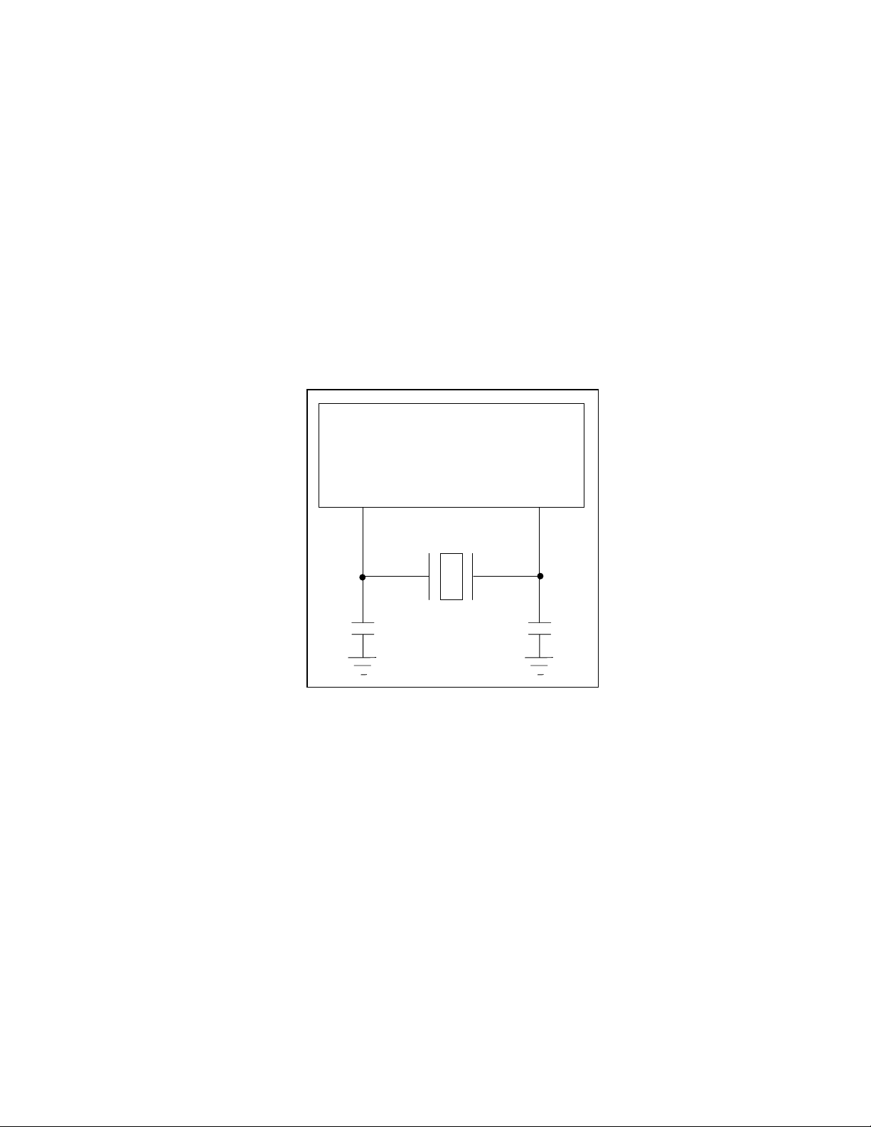
CLOCK GENERATOR
An internal 3.3v crystal oscillator or an external
oscillator source is required for the CAM35C44
(FIGURE 3). The crystal/clock pins and buffer
types are shown in TABLE 1.
The X1/CLK1 and X2 pins provide an external
connection for a parallel resonant 24MHz crystal.
Configuration register CR08 bit 5, INT_OSC,
must be set to “1” to configure the internal
oscillator for this arrangement (see the section
CRO8 - Power Control on page 27).
An external CMOS compatible oscillator is
required if a 24MHz crystal is not used. In this
case INT_OSC must be set to “0”.
FIGURE 3 - EXAMPLE 24MHz OSCILLATOR CIRCUIT
CAM35C44
The X2 pin is the 24MHz crystal driver and
should not be used to drive any other device.
This pin should be left unconnected if an
external clock is used and INT_OSC is “0”.
The 24MHz crystal can be used to directly drive
the ACE block. This saves power when
115.2Kbps or slower data transfers are required
because the PLL and SCE block do not need to
be powered. See TABLE 25 and the section
CRO8 - Power Control on page 27.
X1/CLK1 X2
24MHz CRYSTAL
12
Page 13
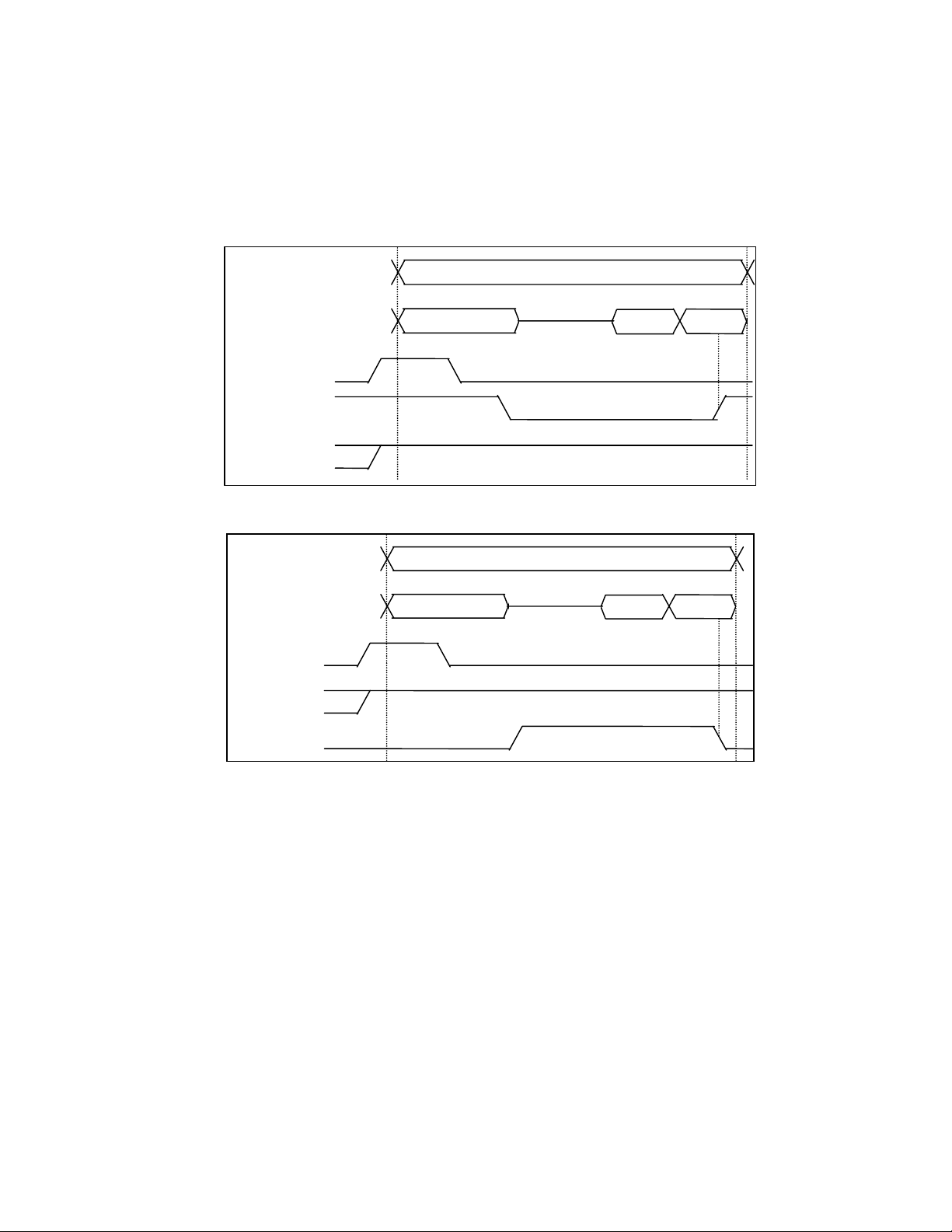
MULTIHOST CPU INTERFACE
The CAM35C44 multihost CPU interface is
capable of supporting three bus configurations;
including, 1) an ISA-style address and data bus,
2) a multiplexed address/data bus with ISA-style
read/write commands like the example shown in
(FIGURE 4, and 3) a multiplexed address/data
FIGURE 4 - NEC UPD781C1X READ CYCLE
bus with a read/write select and data strobe like
the example shown in FIGURE 5.
The CPU interface type as well as the typespecific multiplexing of the processor/host
interface pins (TABLE 1) is controlled by the
Host Interface Select pins.
AB[15:8]
AB[7:0]
ADDR7-ADDR
ADDR15-ADDR
0
8
Data In
ADDR STB
nRD
nWR
AB[15:8]
AB[7:0]
ADDR7-ADD R
ADDR15-ADD R
0
8
Data In
ADDR STB
R/nW
DATA STB
FIGURE 5 - HITACHI HD63P01M1 READ CYCLE
13
Page 14
Host Interface Select
The Host Interface Select pins HS[1:0] (TABLE
1) determine the host interface type.
TABLE 3 - HOST INTERFACE ENCODING
HOST INTERFACE
SELECT
HS1
0 0 Reserved
0 1 ISA
1 0 MULTIPLEXED ADDRESS/DATA, Non-ISA
1 1 MULTIPLEXED ADDRESS/DATA,
Host Interface Pin Multiplexing
Pin multiplexing for the processor/host interface
(TABLE 1) is controlled by the Host Interface
Select pins HS[1:0].
System Data Bus
PIN NAME
SD[7:0] 0 0 NOT DEFINED
0 1 SD[7:0]
1 0 AD[7:0]
1 1 AD[7:0]
HS0
TABLE 4 - SD[7:0] PIN MULTIPLEXING
MUX CONTROLS
HS1
Read/Write (FIGURE 5)
ISA Read/Write (FIGURE 4)
HS0
The encoding for these bits is shown in TABLE
3. The Host Interface Select pins are static
controls and must remain stable during device
operation.
HOST INTERFACE TYPE
ISA signals that are not multiplexed, like
IOCHRDY and nNOWS, remain operative
regardless of the state of the Host Interface
Select bits.
The following tables describe processor/host
interface multiplexing per pin or per pin group.
SELECTED FUNCTION
14
Page 15
ISA Address Bus SA0 - SA1
TABLE 5 - SA[1:0] PIN MULTIPLEXING
PIN NAME
SA[1:0] 0 0 NOT DEFINED
0 1 SA[1:0]
1 0 GPIO[4:3]
1 1 GPIO[4:3]
ISA Address Bus SA2 - SA4
PIN NAME
SA[4:2] 0 0 NOT DEFINED
0 1 SA[4:2]
1 0 BS[2:0]
1 1 BS[2:0]
ISA nIOR
PIN NAME
nIOR 0 0 NOT DEFINED
0 1 nIOR
1 0 R/nW
1 1 nIOR
ISA nIOW
PIN NAME
nIOW 0 0 NOT DEFINED
0 1 nIOW
1 0 DSTRB
1 1 nIOW
MUX CONTROLS
HS1
TABLE 6 - SA[4:2] PIN MULTIPLEXING
MUX CONTROLS
HS1
TABLE 7 - nIOR PIN MULTIPLEXING
MUX CONTROLS
HS1
TABLE 8 - nIOW PIN MULTIPLEXING
MUX CONTROLS
HS1
HS0
HS0
HS0
HS0
SELECTED FUNCTION
SELECTED FUNCTION
SELECTED FUNCTION
SELECTED FUNCTION
15
Page 16

REGISTER ADDRESS MAP
Register addressing in the CAM35C44 is fixed
and requires a 32-byte memory block. Typically,
register addressing is accomplished with a 5 bit
address bus and a 1 bit chip select.
TABLE 9 describes the mapping for the four
register banks in the CAM35C44 address
TABLE 9 - CAM35C44 REGISTER MAP
8-BYTE
ADDRESS
BANK
BANK
SELECT
SA4
BITS
SA3
ADDRESS RANGE
SA[4:0]
0 0 0 0x00 - 0x07 CONFIGURATION
1 0 1 0x08 - 0x0F GPIO
2 1 0 0x10 - 0x17 ACE
3 1 1 0x18 - 0x1F SCE
1
Note
Address Enable (AEN) must be low to access the CAM35C44 registers regardless of the state
of the Host Interface Select bits.
Non-Multiplexed (ISA) Addressing
As shown in TABLE 9 five address bits SA[4:0]
and a chip select nCS are required to access the
CAM35C44 run-time and configuration registers.
In ISA mode, five bits of the ISA System Address
bus SA[4:0] determine the register
space, CONFIGURATION, GPIO, ACE and
SCE, that are required for device configuration
and run-time control.
The external address pins that are responsible
for register addressing will depend on the Host
Interface Select bits (see section MULTIHOST
CPU INTERFACE on page 13).
1
address, while nCS decodes the 32-byte
address block. Note: address block decoding
must be done externally.
The Block Select bits BS[2:0] and two of the
general purpose I/Os GPIO[4:3] are unavailable
in ISA mode.
REGISTER BANK DECODING
16
Page 17

Multiplexed Addressing
When multiplexed address modes are selected,
i.e. HS[1:0] = 02H or 03H (TABLE 3), register
addresses are decoded from the Multiplexed
Address/Data Bus AD[7:0], the Block Select bits
BS[2:0] and the chip select nCS pin.
In the multiplexed addressing modes the 5 loworder bits of the Multiplexed Address/Data Bus
AD[4:0] determine the register address while the
Block Select bits BS[2:0] qualify the
TABLE 10 - EXAMPLE MULTIPLEXED ADDRESS DECODING
256-BYTE
ADDRESS
PAGE
nCS BS2 BS1 BS0 AD[7:0]
1 0 0 1 XXH No Decode: Invalid Page
0 0 0 1 20H Decode Configuration Bank Index
0 0 0 1 00H No Decode: Invalid Block
32-BYTE ADDRESS
BLOCK
MULTIPLEX
ADDR/DATA BUS
three high-order Multiplexed Address/Data Bus
bits, AD[7:5]; i.e., BS[2:0] decodes which of eight
32-byte blocks is selected in the 256-byte page
decoded by nCS. Note: page address decoding
must be done externally.
For example, TABLE 10 illustrates that if BS[2:0]
= 01H, nCS = 0 (active), and AD[7:0] = 20H, the
Index Register in the Configuration Bank has
been selected.
Two extra GPIO pins GPIO[4:3] are available in
the multiplexed address modes.
DESCRIPTION
Register (TABLE 12)
17
Page 18

CONFIGURATION
The CAM35C44 configuration registers are used
to program selectable chip-level device options
(TABLE 13).
The configuration registers can only be
programmed through the configuration access
ports that appear when the chip is placed into
the configuration state.
Configuration register programming typically
follows this sequence:
1. Enter the Configuration State,
2. Program the Configuration
Register(s),
3. Exit the Configuration State.
TABLE 11 - CONFIGURATION ACCESS PORTS
PORT NAME ADDRESS DIRECTION
CONFIG PORT BANK 0, ADDRESS 03 WRITE
INDEX PORT BANK 0, ADDRESS 03 READ/WRITE
DATA PORT BANK 0, ADDRESS 13 READ/WRITE1
1
Note
The INDEX and DATA ports are active only when the CAM35C44 is in the configuration
state.
2
Note
The INDEX PORT is only readable in the configuration state.
3
Note
The CAM35C44 register banks are described in section REGISTER ADDRESS MAP on
page 16. The register addresses in the CAM35C44 configuration bank are shown in
TABLE 12.
If enabled, logical devices in the CAM35C44 will
operate normally in the configuration state.
Configuration Access Ports
The configuration access ports are the config
port, the index port, and the data port (TABLE
11).
The configuration access ports are the only
addressable registers in the CAM35C44
configuration bank (TABLE 12).
The index port and the data port are only active
in the configuration state.
1,2
18
Page 19

Configuration State
Logical devices in the CAM35C44 can operate in
the run state and/or the configuration state. After
power up the CAM35C44 is in the run state, by
default.
To program the configuration registers the
configuration state must be explicitly enabled.
Entering the Configuration State
To enter the configuration state, a configuration
access key must be written to the config port.
The configuration access key is one byte of 55H
data.
Once the configuration access key has been
written to the config port, the CAM35C44
automatically activates the configuration access
ports and enters the configuration state.
Configuration Select Register
The Configuration Select Register (CSR) is
located at the index port address and must be
initialized with the configuration register index
before the register can be accessed using the
data port.
The CSR can only be accessed when the
CAM35C44 is in the configuration state.
Configuration Register Programming
The CAM35C44 contains ten configuration
registers CR00-CR09. After the CAM35C44
enters the configuration state, the configuration
registers are programmed by first writing the
register index number (00 - 09) to the
configuration select register (CSR) and then
writing or reading the configuration register
contents through the data port.
Configuration register access remains enabled
until the configuration state is explicitly exited.
Exiting the Configuration State
To exit the configuration state one byte of AAH
data must be written to the config port.
Once AAH has been written to the config port,
the CAM35C44 automatically deactivates the
configuration access ports and enters the run
state. In the run state, configuration register
access cannot occur until the configuration state
is explicitly re-enabled.
19
Page 20

Programming Example
The following Intel 8086 assembly language instructions illustrate CAM35C44 configuration register
programming. In this example, the config port is located at address 3F0H.
;-----------------------------.
; ENTER CONFIGURATION STATE |
;-----------------------------’
MOV DX,3F0H
MOV AX,055H
OUT DX,AL
;-----------------------------.
; CONFIGURE REGISTERS CR0-CRx |
;-----------------------------’
MOV DX,3F0H
MOV AL,00H
OUT DX,AL ;Point to CR0
MOV DX,3F1H
MOV AL,3FH
OUT DX,AL ;Update CR0
;
MOV DX,3F0H
MOV AL,01H
OUT DX,AL ;Point to CR1
MOV DX,3F1H
MOV AL,9FH
OUT DX,AL ;Update CR1
;
; Repeat for all CRx registers
;
;-----------------------------.
; EXIT CONFIGURATION STATE |
;-----------------------------’
MOV DX,3F0H
MOV AX,AAH
OUT DX,AL
20
Page 21

Configuration Registers
Introduction
The configuration registers (TABLE 13) are set
to their default values at power up and are not
affected by RESET, except where noted in the
register descriptions that follow.
Configuration register bits that are not needed in
the CAM35C44 are marked RESERVED in the
sections below. RESERVED bits cannot be
written and return “0” when read.
TABLE 12 - CONFIGURATION REGISTER BANK
ADDRESS DEFAULT REGISTER NAME
0x00 0x00 Config/Index Register
0x01 0x00 Data Register
0x00 RESERVED
RESET
DEFAULT
Description
CR
INDEX
0x00 0x00 0x00 IRQ CONTROL
0x01 0x00 0x00 DMA CONTROL
0x02 0x02 n/a INFRARED OPTION
0x03 0x01 n/a INFRARED CONTROL B
0x04 0x00 n/a TEST CONTROL A
0x05 0x00 n/a
0x06 0x00 n/a
0x07 0x03 n/a IR HALF DUPLEX TIME-OUT
0x08 0x00 0x00 POWER CONTROL
0x09 0x00 n/a TEST CONTROL B
0x02
.
.
.
0x07
TABLE 13 - CONFIGURATION REGISTERS
POR
DEFAULT
Configuration Register references are in hex;
e.g., CRC0.3 means
Bit
0xC0,
Configuration Bank Addressing
The CONFIGURATION register bank is defined
as the first eight addresses in the CAM35C44
memory map (see section REGISTER
ADDRESS MAP on page 16).
TABLE 12 summarizes the contents of the
CONFIGURATION bank. The Index and Data
registers access the configuration registers
(TABLE 13) as described above.
SOFTWARE SELECT A
SOFTWARE SELECT B
0x03.
REGISTER NAME
Configuration Register
21
Page 22

CR00 - IRQ Control
The IRQ Control register CR00 determines the
IRQ pin polarity and enables the configuration
register locking feature.
CR00 can only be accessed in the
TABLE 14 - IRQ CONTROL REGISTER
CR00 R/W RESERVED LOCK RES IRQ_LEV 0x00
IRQ_LEV, Bit 0
The IRQ_LEV bit D0 determines the active state
of the IRQ output pin (TABLE 1). If IRQ_LEV is
“0” (default), the IRQ pin is active low. If
IRQ_LEV is “1”, the IRQ pin is active high.
LOCK, Bit 2
The LOCK bit D2 selects configuration register
locking. “Locked” means configuration registers
can be read but cannot be written, except for the
IRCC Legacy Controls like the IR HALF
DUPLEX TIME-OUT that can be written through
the SCE Registers and appear in the chip-level
configuration registers regardless of the state of
the LOCK bit.
If LOCK is “0” (default), the configuration
registers are unlocked. If LOCK is “1”, the
configuration registers are locked.
CR01 R/W RESERVED DAC_LEV DREQ_LEV 0x00
D7 D6 D5 D4 D3 D2 D1 D0 DEFAULT
TABLE 15 - DMA CONTROL REGISTER (CR01)
D7 D6 D5 D4 D3 D2 D1 D0 DEFAULT
configuration state and only after the CSR has
been initialized to 00H. The default value of this
register after power up is 00H (TABLE 14).
Bits[7:3, 1] in the IRQ Control register are
RESERVED.
Note: once the LOCK bit is set to “1” the
configuration registers are permanently locked.
The LOCK bit can only be reset to “0” by a hardreset or a power-on-reset; i.e., the configuration
registers cannot be changed until either a hardreset or power-on-reset occur.
CR01 - DMA Control
The DMA Control register CR01 determines the
DRQ and DACK pin polarity (TABLE 1).
CR01 can only be accessed in the configuration
state and only after the CSR has been initialized
to 01H. The default value of this register after
power up is 00H (TABLE 15).
Bits[7:2] in the DMA Control register are
RESERVED.
22
Page 23

DRQ_LEV, Bit 0
The DRQ_LEV bit D0 determines the active
state of the DMA Request (DRQ) output pin
(TABLE 1).
If DRQ_LEV is “0” (default), the DRQ pin is
active low. If DRQ_LEV is “1”, the DRQ pin is
active high.
DAC_LEV, Bit 1
The DAC_LEV bit D1 determines the active state
of the DMA Acknowledge (DACK) input pin
(TABLE 1).
If DAC_LEV is “0” (default), the DACK pin is
active low. If DAC_LEV is “1”, the DACK pin is
active high.
TABLE 16 - INFRARED OPTION REGISTER
CR02 R/W
RCV_POL, Bit 0
The RCV_POL bit D0 defines the active state for
the infrared port receive pins.
If RCV_POL is “0” (default), the IRRX pin is
active low. If RCV_POL is “1”, the IRRX pin is
active high.
The RCV_POL pin has no affect when the port is
configured as a 16C550A UART (see section
IR_MODE, Bits 3 - 5 on page 24).
D7 D6 D5 D4 D3 D2 D1 D0 DEFAULT
RES.
IR_
MODE2
IR_
MODE1
CR02 - Infrared Option
The Infrared Option register CR02 determines
the infrared port transmit and receive pin
polarity, the port duplex mode, and the infrared
port protocol.
The controls in the Infrared Option register are
also duplicated in the IrCC 2.0 SCE
Configuration Register A. These controls are
arranged such that the last write from either
source determines the current control state and
is visible in both registers.
CR02 can only be accessed in the configuration
state and only after the CSR has been initialized
to 02H. The default value of this register after
power up is 02H (TABLE 16).
Bits[7:6] in the Infrared Option register are
RESERVED.
IR_
MODE0
HALF
DUPLEX
XMT_
POL
RCV_
POL
0x02
XMT_POL, Bit 1
The XMT_POL bit D1 defines the active state for
the infrared port transmit pins.
If XMT_POL is “0”, the IRTX pin is active low. If
XMT_POL is “1” (default), the IRTX pin is active
high.
The XMT_POL pin has no affect when the port is
configured as a 16C550A UART (see section
IR_MODE, Bits 3 - 5 on page 24).
23
Page 24

HALF DUPLEX, Bit 2
When the HALF DUPLEX bit D2 is “0” (default),
the 16C550A UART in the IrCC 2.0 is in full
duplex mode. Full duplex mode has no effect on
the IrCC 2.0 SCE.
When the HALF DUPLEX bit is “1”, the IrCC 2.0
is in half duplex mode. Half duplex mode is
typically required for all infrared transactions.
In half duplex mode, the IR Half Duplex TimeOut will apply to IrCC 2.0 transmit/receive
TABLE 17 - CAM35C44 INFRARED PROTOCOL OPTIONS
IR_MODE[2:0]
D5 D4 D3 MODE
0 0 0 COM 16C550A UART (Default)
0 0 1 IrDA SIR-A Up to 115.2Kbps, Variable 3/16ths Pulse
0 1 0 ASK IR 500KHz Carrier, Amplitude Shift Keyed IR
0 1 1 IrDA SIR-B
1 0 0 IrDA HDLC 0.576Mbps and 1.152Mbps
1 0 1 IrDA 4PPM 4Mbps
1 1 0 CONSUMER Consumer (TV Remote) IR
1 1 1 RAW Direct IR Diode Control
CR03 - Infrared Control B
The Infrared Control B register CR03 configures
the infrared interface and COM port clock select.
CR03 can only be accessed in the
CR03 R/W RESERVED MIDI RESERVED HPMODE 0x01
D7 D6 D5 D4 D3 D2 D1 D0 DEFAULT
TABLE 18 - IR CONTROL B REGISTER
direction mode changes (see section CR07 - IR
Half Duplex Time-Out on page 26). The IR Half
Duplex Time-Out does not apply to full duplex
mode.
IR_MODE, Bits 3 - 5
The IR_MODE bits D3 - D5 select the active
IrCC 2.0 encoder/decoder. The default is COM
(TABLE 17).
The IR_MODE bits are equivalent to the three
low-order Block Control bits in the IrCC 2.0 SCE
Configuration Register A.
DESCRIPTION
Up to 115.2Kbps, Fixed 1.6#s Pulse
configuration state and only after the CSR has
been initialized to 03H. The default value of this
register after power up is 01H (TABLE 18).
Bits[7:5,3:1] in the Infrared Control B register are
RESERVED.
24
Page 25

HPMODE, Bit 0
The HPMODE bit D0 is used to configure the
transceiver type in the CAM35C44 infrared
interface (see FIGURE 6). When HPMODE is
“1” (default), the IRMODE/IRRX3 pin is
configured as an input (IRRX3) to support
transceiver types that require two receive
channels. When HPMODE is “0”, the
IRMODE/IRRX3 pin is configured as an output
(IRMODE) to support transceiver types that
require one receive channel and a mode control
pin.
MIDI, Bit 4
The MIDI bit D4 is the 16C550A UART clock
divider select. When MIDI is “0” (default), the
16C550A clock divider is configured to
TABLE 19 - TEST CONTROL A REGISTER
CR04 R/W IR_TEST[6:0] IR_LB 0x00
IR_LB, Bit 0
The IR_LB bit D0 enables serial loopback
testing, independent of the internal IrCC 2.0
loopback controls. When IR_LB is “1” the
transmit output is internally connected to the
receiver input. When IR_LB is “0” (default), the
transmit output is not connected to the receive
input and loopback testing is disabled.
IR_TEST[6:0], Bits 1 - 7
The IR_TEST[6:0] bits D1 - D7 control SMSC
internal test modes.
The IR_TEST[6:0] bits are “0” (default) for
normal operation.
When any of the IR_TEST[6:0] bits are “1”, an
SMSC internal test mode is activated. Note:
SMSC internal test modes are reserved for
D7 D6 D5 D4 D3 D2 D1 D0 DEFAULT
generate the standard UART data rates up to
115.2Kbaud.
When MIDI is “1”, the 16C550A clock divider is
configured to generate UART data rates that are
compatible with the 31.25Kbaud ($1%) Musical
Instrument Digital Interface standard.
CR04 - Test Control A
The Test Control A register CR04 enables userlevel serial loopback testing and SMSC internal
test modes.
CR04 can only be accessed in the configuration
state and only after the CSR has been initialized
to 04H. The default value of this register after
power up is 00H (TABLE 19).
SMSC use, only. Activating SMSC internal test
modes may produce undesired results.
CR05 - Software Select A
The Software Select A register CR05 is directly
connected to the read-only IrCC 2.0 Software
Select A register in SCE Register Block Three.
Writing to CR05 is the only way to revise the
contents of the Software Select A register.
CR05 can only be accessed in the configuration
state and only after the CSR has been initialized
to 05H. The default value of this register after
power up is 00H (TABLE 20).
25
Page 26

TABLE 20 - SOFTWARE SELECT A REGISTER
CR05 R/W Software Select A 0x00
CR06 - Software Select B
The Software Select B register CR06 is directly
connected to the read-only IrCC 2.0 Software
Select B register in SCE Register Block Three.
Writing to CR06 is the only way
CR06 R/W Software Select B 0x00
CR07 - IR Half Duplex Time-Out
CR07 is the IR Half Duplex Time-Out register
(TABLE 22).
If the Half Duplex option is selected (see section
HALF DUPLEX, Bit 2 on page 24), the IR half
duplex time-out constrains the timing of
transmit/receive direction mode changes in the
IrCC 2.0. The IR half duplex time-out is started
as each IR message data bit is transferred and
prevents direction mode changes until the timeout expires. The timer is restarted whenever
new data is transferred in the current direction
mode.
For example, in an SIR mode if data is loaded
into the transmit buffer while a character is being
received, the transmission will not start
CR07 R/W IR HALF DUPLEX TIME-OUT 0x03
D7 D6 D5 D4 D3
to revise the contents of the Software Select B
register. CR06 can only be accessed in the
configuration state and only after the CSR has
been initialized to 06H. The default value of this
register after power up is 00H (TABLE 21).
TABLE 21 - SOFTWARE SELECT B REGISTER
D7 D6 D5 D4
D3
until the last bit has been received and the timeout expires. If the start bit of another character
is received during this time-out, the timer is
restarted after the new character is received.
The IRCC block i n the CAM35C44 also incl udes
an 8 bit IR half duplex time-out register, like
CR07, in SCE Register Block 5. These two
registers behave like the other IRCC legacy
controls where either source uniformly updates
the value of both registers when either register is
explicitly written using IOW or following a devicelevel POR. IRCC software resets d o not affect
these registers.
The IR half duplex time-out is programmable
from 0 to 25.5ms in 100#s increments, as
follows:
IR HALF DUPLEX TIME-OUT = (CR07) x 100
TABLE 22 - IR HALF DUPLEX TIME-OUT REGISTER
D7
D6
D5
D4
D2 D1 D0 DEFAULT
D2
D3
D1
D2
####
s
D1
D0
D0 DEFAULT
DEFAUL
T
26
Page 27

CR08 - Power Control
The Power Control register CR08 contains the
power control enables to select the various
CAM35C44 power states (TABLE 25) and also
includes a bit to configure the system clock
TABLE 23 - POWER CONTROL REGISTER
CR08 R/W
OSC_ON, Bit 0
The OSC_ON bit D0 determines the power state
for CAM35C44 clock generator, independent of
the clock source (see section INT_OSC, Bit 5 on
page 28). When OSC_ON is “0” (default), the
clock generator is powered down. When
OSC_ON is “1”, the clock generator is running.
ACE_ON, Bit 1
The ACE_ON bit D1 along with the AUTO_PWR
bit D4 determines the power state for IrCC 2.0
ACE UART. When ACE_ON is “0” (default), the
UART is powered down, regardless of the state
of AUTO_PWR; i.e., when ACE_ON is “0”,
UART wake-up events are disabled (see section
AUTO_PWR, Bit 4). When ACE_ON is “1”, the
UART is active.
PLL_ON, Bit 2
The PLL_ON bit D2 determines the power state
for the PLL clock multiplier. The PLL is required
for IrDA transfers above 115.2Kbps. When
PLL_ON is “0” (default), the PLL is powered
down. When PLL_ON is “1”, the PLL is running.
D7 D6 D5 D4 D3 D2 D1 D0
RES
INT_
OSC
AUTO_
PWR
source. CR08 can only be accessed in the
configuration state and only after the CSR has
been initialized to 08H. The default value of this
register after power up is 00H (TABLE 23).
Bits[7:6] in the Power Control register are
RESERVED.
Default
SCE_
ON
PLL_
ON
ACE_ON OSC_ON 0x00
SCE_ON, Bit 3
The SCE_ON bit D3 determines the power state
for the IrCC 2.0 SCE. The SCE is required for
IrDA transfers above 115.2Kbps and for all
Consumer IR transactions. When SCE_ON is
“0” (default), the SCE is powered down. When
SCE_ON is “1”, the SCE is active.
AUTO_PWR, Bit 4
The AUTO_PWR bit D4 along with the ACE_ON
bit D1 selects the auto power down state of the
ACE UART (TABLE 24). When AUTO_PWR is
“0” (default), the ACE auto power down state is
disabled and the ACE UART power state is
controlled solely by the ACE_ON bit (see section
ACE_ON, Bit 1 on page 27). Note: If the ACE
auto power state is disabled the ring indicator
(nRI) and the RXD power-on wake-up events are
disabled. When AUTO_PWR is “1” and
ACE_ON is “1”, the ACE auto power down state
is enabled and the following power management
events are possible.
27
Page 28

Transmitter Auto Power Down
The UART transmitter is powered down from the
auto power down state when the transmit buffer
and transmit shift registers are empty.
Receiver Auto Power Down
The UART receiver is powered down from the
auto power state when the receive FIFO is
empty and the receiver is waiting for a start bit.
TABLE 24 - ACE UART POWER STATES
ACE_ON
(D1)
0 X ACE POWER OFF
1 0 ACE POWER ON
1 1 ACE AUTO POWER DOWN
INT_OSC, Bit 5
The INT_ OSC bit D5 selects the clock source
for the CAM35C44 clock generator (see section
CLOCK GENERATOR on page 12).
AUTO_PWR
(D4)
Ring Indicator Auto Power Down
When the UART is powered down from the auto
power state, a Ring Indicator interrupt can occur
on active transitions of the Ring Indicator input
nRI.
Exit Auto Power Down
The transmitter exits the auto power down state
on a write to the transmit buffer. The receiver
exits the auto power down state when the
receiver input RXD changes state.
DESCRIPTION
When INT_OSC is “0” (default), the clock
generator is driven by an external clock source.
When INT_OSC is “1”, the clock generator is
driven by the internal crystal oscillator.
28
Page 29

TABLE 25 - EXAMPLE POWER CONSUMPTION VS. POWER CONTROL ENABLES
CR08[3:0]
D3 D2 D1 D0
0 0 0 0
0 0 0 1
0 0 1 1
0 1 1 1
1 1 1 1
1
Note
: The 24MHz crystal oscillator directly driving the ACE block enables data transfers up to
115.2Kbps.
2
Note
: The PLL driving the SCE block enables data transfers up to 4Mbps.
3
Note
: PW RGD does not stop the crystal from oscillating if OSC_ON, D0 in configuration register
CR08, is “1”.
4
Note
: PWRGD i s “0”.
5
Note
: PWRGD i s “1”.
CR09 - Test Control B
The IR_TEST[14:7] bits D0 - D7 in the Test
Control B register enable SMSC internal test
modes. CR09 can only be accessed in the
configuration state and only after the CSR has
been initialized to 09H. The default value of this
register after power up is 00H (TABLE 26). The
IR_TEST[14:7] bits are “0” (default)
CR09 R/W IR_TEST[14:7] 0x00
POWER
CONSUMPTION
(ICC)
TYP MAX
1
#
2
#
(Note
500
A4
A5
#
3
A
)
2.5
#
5
#
(Note
1mA
A4
A5
3
)
1mA 2mA
1.6mA 3mA
6mA 8mA
CLOCK
GENERATOR BLOCK
ACE
1
PLL BLOCK2
OFF OFF OFF OFF
RUNNING OFF OFF OFF
RUNNING ON OFF OFF
RUNNING ON
RUNNING ON
RUNNING
RUNNING
for normal operation. When any of the
IR_TEST[14:7] bits are “1”, an SMSC internal
test mode is activated. Note: SMSC internal test
modes are reserved for SMSC use, only.
Activating SMSC internal test modes may
produce undesired results.
TABLE 26 - TEST CONTROL B REGISTER
D7 D6 D5 D4 D3 D2 D1 D0 DEFAULT
SCE
OFF
ON
29
Page 30

INFRARED INTERFACE
The CAM35C44 infrared interface can support
various infrared protocols and transceiver
configurations. For more information consult the
SMSC Infrared Communication Controller (IrCC
2.0) specification.
IrDA SIR/FIR
IrDA SIR (v1.0) specifies asynchronous serial
communication at baud rates up to 115.2kbps.
Each byte is sent serially LSB first beginning
with a zero value start bit. A zero is signaled by
sending a single infrared pulse at the beginning
of the serial bit time. A one is signaled by the
absence of an infrared pulse during the bit time.
IrDA FIR (v1.1) includes IrDA v1.0 SIR and
additionally specifies synchronous serial
communications at data rates up to 4Mbps.
Data is transferred LSB first in packets that can
be up to 2048 bits in length. IrDA v1.1 includes
.576Mbps and 1.152Mbps data rates using an
encoding scheme that is similar to SIR. The
4Mbps data rate uses a pulse position
modulation (PPM) technique.
ASKIR
The ASKIR infrared protocol allows
asynchronous amplitude shift keyed serial
communication at baud rates up to 19.2kbps.
TABLE 27 - TRANSCEIVER MODULE INTERFACE TYPE SELECT
HP MODE (CR03.0) FUNCTION
0 IR Mode
1 IRRX3
Each byte is sent serially LSB first beginning
with a zero value start bit. A zero is signaled by
sending a 500kHz carrier waveform for the
duration of the serial bit time. A one is signaled
by the absence of carrier during the bit time.
Consumer IR
The CAM35C44 Consumer IR interface is a
general-purpose synchronous amplitude shift
keyed encoder/decoder with programmable
carrier and bit-cell rates that can emulate many
popular TV Remote encoding formats; including,
38kHz PPM, PWM and RC-5. Each bit is sent
serially LSB first. The carrier frequency is
programmable from 1.6MHz to 6.25kHz. The
bit-cell rate range is 100kHz to 390Hz.
Hardware Interface
The CAM35C44 IR hardware interface is shown
in FIGURE 6. This interface supports two types
of IR transceiver modules. One interface type
requires a mode pin (IR Mode) to select the data
rate, while the other interface type requires a
second Rx data pin (IRRX3). The transceiver
interface type is selected with the HPMODE bit
D0 in CR03 as shown in TABLE 27 (see section
HPMODE, Bit 0 on page 25).
30
Page 31

(
)
The FAST bit in FIGURE 6 is used to select
between an SIR mode and FIR mode receiver,
regardless of the transceiver type. If FAST is
TABLE 28 - IR RX DATA PIN SELECTION
CONTROL SIGNALS
FAST HPMODE RX1 RX2
0 X RXD2 IRRX2
X 0 RXD2 IRRX2
1 1 IR MODE/IRRX3 IR MODE/IRRX3
FIGURE 6 - IR INTERFACE BLOCK DIAGRAM
“1”, the FIR mode receiver is selected; if FAST is
“0”, the SIR mode receiver is selected (TABLE
28).
INPUTS
RAW
TV
ASK
SIR
COM
IR
RX1
RX2
TX1
0
1
TX2
0
1
TXD2
RXD2
IRTX
IRRX
FIR
aux
COM
G.P. DATA
FAST BIT
FAST
IRMODE
HPMODE
IRMODE
/IRRX3
IrCC 2.0
31
Page 32

GENERAL PURPOSE I/O
Introduction
The CAM35C44 can support up to 5 general
purpose I/O pins, GPIO[4:0] (TABLE 1). The
number of available general purpose I/O pins
TABLE 29 - GPIO REGISTER BANK MAP
BANK ADDRESS DEFAULT REGISTER NAME
BANK 1 0x00 0x00 GPIOA Enable Register
(GPIO) 0x01 0x00 RESERVED
0x02 0x00 GPIOA Data Register
0x03 0x00 RESERVED
0x04 0x00 GPIOA Direction Register
0x05 0x00 RESERVED
0x06 0x00 RESERVED
0x07 0x00 RESERVED
Description
The state of a GPIO pin can be forced to the
value contained its data register, depending on
the state of its direction and enable bits. For
example, when a GPIO pin is configured as an
output the data register contains a “1” and the
enable bit is active, the GPIO pin will be driven
high. When a GPIO pin is configured as an input
and the enable is active, the value in the data
register will reflect the state of the
depends upon the Host Interface Select bits (see
the section MULTIHOST CPU INTERFACE on
page 13). The general purpose I/O pins are
controlled by the GPIO registers contained in
Bank 1 of the CAM35C44 memory map (see the
section REGISTER ADDRESS MAP on page
16). TABLE 29 summarizes the contents of the
GPIO register bank.
pin. When a GPIO pin is configured as an input
and the enable is inactive, state changes at the
pin are not reflected in the data register. W hen
a GPIO pin is configured as an output and the
enable is inactive, changes in the data register
do not affect the pin. TABLE 12 summarizes the
GPIO pin behavior described above. FIGURE 7
illustrates GPIO pin functionality. Note: FIGURE
7 is for illustration purposes only and is not
intended to suggest specific implementation
details.
32
Page 33

TABLE 30 - GPIO FUNCTIONAL DESCRIPTION
GPx
ENABLE
1
1 1 OUTPUT READ CURRENT
WRITE NEW VALUE Output pin is active (driven),
1 0 INPUT READ CURRENT
WRITE NO EFFECT Input pin is active, writes
0 1 INPUT READ LAST VALUE Output pin is floating, reads
WRITE NEW VALUE Output pin is floating, writes
0 0 INPUT READ LAST VALUE Input pin is disabled, reads
WRITE NO EFFECT Input pin is disabled, writes
Note1 This represents a GPIO Enable register bit. The GPIO Enable register is GP00 (see section
GPIOA Enable Register on page 34).
2
Note
This represents a GPIO Direction register bit. The GPIO Direction register is GP04 (see
section GPIOA Direction Register on page 35).
3
Note
This represents a GPIO Data register bit. The GPIO Data register is GP02 (see section
GPIOA Data Register on page 35).
GPx
OUT2
GPIOx PIN
DIRECTION
I/O
COMMAND
GPx
DATA3
VALUE
VALUE
DESCRIPTION
Output pin is active (driven),
reads return last write.
writes update data register.
Input pin is active, reads
return the current state of the
pin.
have no effect.
return last active state.
update data register.
return last enabled read
state.
have no effect.
33
Page 34

GPx_OUT
GPx_EN
GPx_DAT
DQ
D-TYPE
GPx_nIOW
CLK
GPx_nIOR
FIGURE 7 - GENERAL PURPOSE I/O BLOCK DIAGRAM
Note:
This figure is for illustration purposes only and is not intended to suggest specific
implementation details)
Registers
GPIOA Enable Register
The GPIOA Enable register GP00 contains the
enable bits for the five general purpose I/O pins
(TABLE 31). When any of the GPx_EN bits are
“1”, the associated general purpose I/O pin is
enabled. When any of the GPx_EN bits are “0”,
the associated general purpose
GP00 R/W
D7 D6 D5 D4 D3 D2 D1 D0 DEFAULT
RESERVED
TABLE 31 - GPIOA ENABLE REGISTER
GP4_
EN
GP3_
EN
1
GPIOx
DQ
TRANS-
PARENT
0
G
I/O pin is disabled. The affects of the GPx_EN
bits are summarized in TABLE 30. GP00 can be
accessed both in the configuration state and the
run state (see section REGISTER ADDRESS
MAP on page 16 and TABLE 29). The default
value of the GPIOA Enable register after power
up is 00H. Bits[7:5] in the GPIOA Enable
register are RESERVED.
GP2_
EN
GP1_
EN
GP0_
EN
0x00
34
Page 35

GPIOA Data Register
The GPIOA Data register GP02 contains the
data bits for the five general purpose I/O pins
(TABLE 32). The state of a GPIO pin can be
forced to the value contained its data register, or
the value in the data register can reflect the state
of the pin, depending on the state of the
direction and enable bits. The affects of the
TABLE 32 - GPIOA DATA REGISTER
GP02 R/W
D7 D6 D5 D4 D3 D2 D1 D0 DEFAULT
RESERVED
GP4_
DAT
GPIOA Direction Register
The GPIOA Direction register GP04 contains the
direction bits for the five general purpose I/O
pins (TABLE 33). The direction of a GPIO pin
depends upon the state of the direction bit and
the enable bit, but typically if the direction bit is
“1” the GPIO pin is an output; if the direction bit
is “0” the GPIO pin is an input.
TABLE 33 - GPIOA DIRECTION REGISTER
GP04 R/W
D7 D6 D5 D4 D3 D2 D1 D0 DEFAULT
RESERVED
GP4_
OUT
GP3_
OUT
GPx_DAT bits are summarized in TABLE 30.
GP02 can be accessed both in the configuration
state and the run state (see section REGISTER
ADDRESS MAP on page 16 and TABLE 29).
The default value of the GPIOA Data register
after power up is 00H. Bits[7:5] in the GPIOA
Data register are RESERVED.
GP3_
DAT
GP2_
DAT
GP1_
DAT
GP0_
DAT
0x00
The affects of the GPx_OUT bits are
summarized in TABLE 33. GP04 can be
accessed both in the configuration state and the
run state (see section REGISTER ADDRESS
MAP on page 16 and TABLE 29). The default
value of the GPIOA Direction register after
power up is 00H. Bits[7:5] in the GPIOA
Direction register are RESERVED.
GP2_
OUT
GP1_
OUT
GP0_
OUT
0x00
35
Page 36

DC ELECTRICAL CHARACTERISTICS
(TA = 0°C - 70°C4, Vcc = +3.3 V ± 10%)
Note: Numbers appearing in parentheses represent the values for TXD/IRTX, IRTX,
IRMODE/IRRX3 when VIO is 5 Volt.
PARAMETER SYMBOL MIN TYP MAX UNITS COMMENTS
I Type Input Buffer
Low Input Level
High Input Level
IS Type Input Buffer
Low Input Level
High Input Level
Schmitt Trigger Hysteresis
I
Input Buffer
CLK
Low Input Level
High Input Level
Input Leakage
(All I and IS buffers except
PWRGD)
Low Input Leakage
High Input Leakage
Input Current
PWRGD
IO12 Type Buffer
Low Output Level
High Output Level
Output Leakage
V
V
V
V
V
V
V
HYS
ILCK
IHCK
I
I
IOH
V
V
I
OL
ILI
IHI
ILIS
IHIS
IL
IH
OL
OH
0.8
2.0
2.2
250
0.8
0.4
2.8
-10
-10
2.4
-10
+10
+10
75
150
0.4
+10
V
V
V
V
mV
V
V
µA
µA
µA V
V
V
µA
TTL Levels
Schmitt Trigger
Schmitt Trigger
V
= 0
IN
V
= Vcc
IN
= 0
IN
I
= 12mA (24mA)
OL
I
= -6mA (-12mA)
OH
V
= 0 to V
IN
(Note 1)
cc
36
Page 37

PARAMETER SYMBOL MIN TYP MAX UNITS COMMENTS
O12 Type Buffer
Low Output Level
High Output Level
Output Leakage
O12PD Type Buffer
Low Output Level
High Output Level
Output Leakage
O
Type Buffer
CLK
Low Output Level
High Output Level
Output Leakage
OD12 Type Buffer
Low Output Level
Output Leakage
Supply Current Activ e
Supply Current Standby
V
V
I
V
V
I
V
V
I
V
I
ICC
I
CSBY
OL
OH
OL
OL
OH
OL
OL
OH
OL
OL
OL
2.4
-10
2.4
-10
2.2
-10
-10
0.4
+10
0.4
+10
0.4
+10
0.4
+10
8
2.5
TABLE 34 - DC ELECTRICAL CHARACTERISTICS
Note 1: All output leakages are measured with the current pins in high impedance as defined by the
PWRGD pin.
Note 2: Output leakage is measured with the low driving output off, either for a high level output or
a high impedance state defined by PWRGD.
Note 3: Defined by the device configuration with the PWRGD input low.
Note 4: Junction Temperature rise at 70°C ambient will be approximately 1.7°C. Junction Temperature
rise = Ambient Temp. +0
ja x Max. Power; where 0ja = 56.8 and Max. Power = 3.6V x 8mA
V
V
µA
V
V
µA
V
V
µA
V
µA
mA
µA
I
= 12mA
OL
I
= -6mA
OH
V
= 0 to Vcc (Note 1)
IN
I
= 12mA (24mA)
OL
I
= -6mA (-12mA)
OH
V
= 0 to Vcc (Note 1)
IN
I
= 2mA
OL
I
= -2mA
OH
V
= 0 to Vcc (Note 1)
IN
I
= 12 mA
OL
V
= 0 to Vcc (Note 1)
IN
All outputs open.
Note 3
37
Page 38

A.C. TIMING
X1/CLK1
Clock and Reset Timing
RESET DRV
TABLE 35 - CRYSTAL AND RESET TIMING PARAMETERS
NAME DESCRIPTION MIN TYP MAX UNITS
tcyc Clock Cycle Time 37 41 45 ns
txl Clock Low Pulse Width 18.5 20.5 22.5 ns
trst Reset Pulse Width 10 us
tcyc
txltxl
FIGURE 8 - EXTERNAL CLOCK INPUT TIMING
trsttrst
FIGURE 9 - RESET_DRV PULSE TIMING
38
Page 39

Read Cycle Timing (Non-Multiplexed)
SA[4:0]
nCS
t5
t1
nRD
SD[7:0]
FIGURE 10 - READ CYCLE (NON-MULTIPLEXED ADDRESS AND DATA)
t3t3
t2 t4
TABLE 36 - READ CYCLE TIMING PARAMETERS (NON-MULTIPLEXED ADDRESS AND DATA)
NAME DESCRIPTION MIN TYP MAX UNITS
t1 Chip Select and Address Valid to Read
15 ns
Pulse Active
t2 Read Pulse Active to Data Valid 0 55 ns
t3 Read Pulse Width 85 ns
t4 Data Hold Time 5 ns
t5
Note 1
Read Pulse Active to Chip Select and
Address Invalid
15 ns
Note 1: Chip select must be latched internally and released when read pulse goes inactive.
39
Page 40

Read Cycle Timing (Multiplexed)
nCS
ASTRB
nRD
t4 t9
t1
t8t8
t5
t10
t3t3
AD[7:0]
Address Data
t7 t2 t6
FIGURE 11 - READ CYCLE (MULTIPLEXED ADDRESS AND DATA)
TABLE 37 - READ CYCLE TIMING PARAMETERS (MULTIPLEXED ADDRESS AND DATA)
NAME DESCRIPTION MIN TYP MAX UNITS
t1 Address Strobe Setup Time 30 ns
t2 Read Pulse Active to Data Valid 55 ns
t3 Read Pulse Width 85 ns
t4 Address Strobe Inactive to Chip Select Active 0 8 ns
t5 Chip Select Active to Read Pulse Active 15 ns
t6 Data Hold Time 5 ns
t7 Address Strobe Hold Time 5 15 ns
t8 Address Strobe Pulse Width 23 ns
t9
Read Pulse Active to Chip Select Inactive 15 ns
Note 1
t10 Address Strobe Inactive to Read Pulse
15
Active
Note 1: Chip select must be latched internally and released when read pulse goes inactive.
40
Page 41

Write Cycle Timing (Non-Multiplexed)
SA[4:0]
t5
nCS
t3t3
t1 t4
nWR
t2
SD[7:0]
FIGURE 12 - WRITE CYCLE (NON-MULTIPLEXED ADDRESS AND DATA)
TABLE 38 - WRITE CYCLE TIMING PARAMETERS (NON-MULTIPLEXED ADDRESS AND DATA)
NAME DESCRIPTION MIN TYP MAX UNITS
t1 Chip Select and Address Valid to Write Pulse
23 ns
Active
t2 Data Hold Time 8 ns
t3 Write Pulse Width 85 ns
t4 Data valid to Write Pulse Inactive 30 ns
t5
Note 1
Write Pulse Active to Chip Select and Address
Invalid
15 ns
Note 1: Chip select must be latched internally and released when write pulse goes inactive.
41
Page 42

Write Cycle Timing (Multiplexed)
nCS
ASTRB
t7 t9
t1
t8
t3t3
nWR
AD[8:0]
t5
t10 t4
t2 t6
Address Data
FIGURE 13 - WRITE CYCLE (MULTIPLEXED ADDRESS AND DATA)
TABLE 39 - WRITE CYCLE TIMING PARAMETERS (MULTIPLEXED ADDRESS AND DATA)
NAME DESCRIPTION MIN TYP MAX UNITS
t1 Address Strobe Setup Time 30 ns
t2 Address Strobe Hold Time 8 15 ns
t3 Write Pulse Width 85 ns
t4 Data Valid to Write Pulse Inactive 30 ns
t5 Chip Select Active to Write Pulse Active 15 ns
t6 Data Hold Time 5 ns
t7 Address Strobe Inactive to nCS Active 0 5 ns
t8 Address Strobe Pulse Width 23 ns
t9
Write Pulse Active to Address Strobe Inactive 15 ns
Note 1
t10 Address Strobe Inactive to Write Pulse Active 10
Note 1: Chip select must be latched internally and released when write pulse goes inactive.
42
Page 43

A
A
AD[
]
Read/Write Cycle Timing (Multiplexed)
nCS
t1
t8
STRB
R/nW
t7 t9
t5
t3t3
t10 t4
DSTRB
t2 t6
8:0
FIGURE 14 - READ/WRITE CYCLE (MULTIPLEXED ADDRESS AND DATA)
TABLE 40 - READ/WRITE CYCLE TIMING PARAMETERS (MULTIPLEXED ADDRESS AND DATA)
NAME DESCRIPTION MIN TYP MAX UNITS
t1 Address Strobe Setup Time 30 ns
t2 Address Strobe Hold Time 8 15 ns
t3 Data Strobe Pulse Width 85 ns
t4 Data Valid to R/nW Pulse Inactive 30 ns
t5 Chip Select Active to R/nW Pulse Active 15 ns
t6 Data Hold time 5 ns
t7 Address Strobe Inactive to nCS Active 0 5 ns
t8 Address Strobe Pulse Width 23 ns
t9
Note 1
t10 Address Strobe Inactive to R/nW Pulse Active 10
Note 1: Chip select must be latched internally and released when write pulse goes inactive.
R/nW Pulse Active to Address Strobe Inactive 15 ns
ddress Data
43
Page 44

Single Transfer Mode DMA Timing
AEN
DRQ
t15
t3
t2
t16
nDACK
nRD or nWR
AD[7:0]
TC
t1
t19
t6
t5
t14 t8
t11
t17t17
t7 t9
t13t13
t12
FIGURE 15 - SINGLE TRANSFER MODE DMA TIMING
Refer to table on the following page.
t4t4
t18t18
t10
44
Page 45

TABLE 41 - SINGLE TRANSFER MODE DMA TIMING PARAMETERS
NAME DESCRIPTION MIN TYP MAX UNITS
t1 nDACK Delay Time from DRQ High 0 ns
t2 DRQ Reset Delay from nRD or nWR 15 ns
t3 DRQ Reset Delay from nDACK Low 15 ns
t4 nDACK Inactive 30 ns
t5 nRD Delay from DRQ High 15 ns
t6 nWR Delay from DRQ High 15 ns
t7 Data Access Time from nRD Low 55 ns
t8 Data Set Up Time to nWR High 30 ns
t9 Data to Float Delay from nRD High 5 ns
t10 Data Hold Time from nWR High 5 ns
t11 nDACK Set Up to nWR/nRD Low 5 ns
t12 nDACK Hold after nWR/nRD High 5 ns
t13 TC Pulse Width 30 ns
t14 AEN Set Up to nRD/nWR 30 ns
t15 AEN Hold from nDACK 0 ns
t16 TC Active to DRQ Inactive 15 ns
t17 nRD/nWR Pulse Width 85 ns
t18 nRD/nWR Inactive 30 ns
t19 AEN Active to nDACK Active 0 ns
45
Page 46

Burst Transfer Mode DMA Timing
AEN
DRQ
t1
nDACK
nRD or nWR
t19 t12
t11
t6
t5
t14
t17
t15
t3
t18
t2
t16
t4
t8
AD[7:0]
TC
t7 t9
t13
FIGURE 16 - BURST TRANSFER MODE DMA TIMING
Refer to table on the following page.
t10
46
Page 47

TABLE 42 - DMA TIMING (BURST TRANSFER MODE) PARAMETERS
NAME DESCRIPTION MIN TYP MAX UNITS
t1 nDACK Delay Time from DRQ High 0 ns
t2 DRQ Reset Delay from nRD or nWR 15 ns
t3 DRQ Reset Delay from nDACK Low 15 ns
t4 nDACK Inactive 30 ns
t5 nRD Delay from DRQ High 15 ns
t6 nWR Delay from DRQ High 15 ns
t7 Data Access Time from nRD Low 55 ns
t8 Data Set Up Time to nWR High 30 ns
t9 Data to Float Delay from nRD High 5 ns
t10 Data Hold Time from nWR High 5 ns
t11 nDACK Set Up to nWR/nRD Low 5 ns
t12 nDACK Hold after nWR/nRD High 5 ns
t13 TC Pulse Width 30 ns
t14 AEN Set Up to nRD/nWR 15 ns
t15 AEN Hold from nDACK 0 ns
t16 TC Active to DRQ Inactive 15 ns
t17 nRD/nWR Pulse Width 85 ns
t18 nRD/nWR Inactive 30 ns
t19 AEN Active to nDACK Active 0 ns
47
Page 48

FIGURE 17 - 48 PIN TQFP PACKAGE OUTLINE
MIN NOMINAL MAX REMARK
A ~ ~ 1.6 Overall Package Height
A1 0.05 0.10 0.15 Standoff
A2 1.35 1.40 1.45 Body Thickness
D ~ 9.00 ~ X Span
D/2 4.40 4.50 4.60 1/2 X Span Measure from Centerline
D1 ~ 7.00 ~ X body Size
E ~ 9.00 ~ Y Span
E/2 4.40 4.50 4.60 1/2 Y Span Measure from Centerline
E1 ~ 7.00 ~ Y body Size
H 0.09 ~ 0.20 Lead Frame Thickness
L 0.45 0.60 0.75 Lead Foot Length from Centerline
L1 ~ 1.00 ~ Lead Length
e 0.50 Basic Lead Pitch
%"
o
~ 7o Lead Foot Angle
0
W 0.17 ~ 0.27 Lead Width
R1 0.08 ~ ~ Lead Shoulder Radius
48
Page 49

MIN NOMINAL MAX REMARK
R2 0.08 ~ 0.20 Lead Foot Radius
ccc ~ ~ 0.0762 Coplanarity (Assemblers)
ccc ~ ~ 0.08 Coplanarity (Test House)
Note 1: Controlling Unit: millimeter
Note 2: Tolerance on the position of the leads is ± 0.04 mm maximum.
Note 3: Package body dimensions D1 and E1 do not include the mold protrusion. Maximum mold
protrusion is 0.25 mm.
Note 4: Dimension for foot length L measured at the gauge plane 0.25 mm above the seating plane is
0.78-1.08 mm.
Note 5: Details of pin 1 identifier are optional but must be located within the zone indicated.
CAM35C44 ERRATA SHEET
PAGE
1 GENERAL DESCRIPTION 24mA changed to 12mA 1/7/98
10 DESCRIPTION OF PIN
21 TABLE 13/REGISTER NAME See Italicized Text 1/7/98
29 TABLE 25 See Italicized Text 1/7/98
37 Note 4 added See Italicized Text 1/7/98
29 TABLE 25
37 TABLE 34 – MAX Column See Italicized Text 8/10/99
SECTION/FIGURE/ENTRY
FUNCTIONS
CORRECTION
See Italicized Text 1/7/98
2#A changed to 2.5#A
DATE
REVISED
8/10/99
49
Page 50

© 2000 STANDARD MICROSYSTEMS CORPORATION (SMSC)
80 Arkay Drive
Hauppauge, NY 11788
(631) 435-6000
FAX (631) 273-3123
Standard Microsystems is a registered trademark of Standard Microsystems Corporation, and SMSC is a trademark of Standard
Microsystems Corporation. Product names and company names are the trademarks of their respective holders. Circuit diagrams
utilizing SMSC products are included as a means of illustrating typical applications; consequently complete information sufficient for
construction purposes is not necessarily given. Although the information has been checked and is believed to be accurate, no
responsibility is assumed for inaccuracies. SMSC reserves the right to make changes to specifications and product descriptions at any
time without notice. Contact your local SMSC sales office to obtain the latest specifications before placing your product order. The
provision of this inform ation does not convey to the purchaser of the sem iconductor devices described any licenses under the patent
rights of SMSC or others. All sales are expressly conditional on your agreement to the terms and conditions of the most recently dated
version of SMSC's standard Terms of Sale Agreement dated before the date of your order (the "Terms of Sale Agreement"). The
product may contain design defects or errors k nown as anomalies which may cause the product's functions to deviate from published
specifications. Anomaly sheets are available upon request. S MSC products are not designed, intended, authorized or warranted for
use in any life support or other application where product failure could cause or contribute to personal injury or severe property
damage. Any and all such uses without prior written approval of an Officer of S MSC and further testing and/or m odifi cation wil l be fully
at the risk of the customer. Copies of this document or other SMSC literature, as well as the Terms of Sale Agreement, may be
obtained by visiting SMSC’s website at http://www.smsc.com.
SMSC DISCLAIMS AND EXCLUDES ANY AND ALL WARRANTIES, INCLUDING WITHOUT LIMITATION ANY AND ALL IMPLIED
WARRANTIES OF MERCHANTABILITY, FITNESS FOR A PARTICULAR PURPOSE, TITLE, AND AGAINST INFRINGEMENT,
AND ANY AND ALL WA RRANTIES ARISING FROM ANY COURSE OF DEALING OR USAGE OF TRADE.
IN NO EVENT SHALL SMSC BE LIABLE FOR ANY DIRECT, INCIDENTAL, INDIRECT, SPECIAL, PUNITIVE, OR
CONSEQUENTIAL DAMAGES; OR FOR LOST DATA, PROFITS, SAVINGS OR REVENUES OF ANY KIND; REGARDLESS OF
THE FORM OF ACTION, WHETHER BASED ON CONTRACT; TORT; NEGLIGENCE OF SMSC OR OTHERS; STRICT LIABILITY;
BREACH OF WARRANTY; OR OTHERWISE; WHETHER OR NOT ANY REMEDY IS HELD TO HAVE FAILED OF ITS ESSENTIAL
PURPOSE, AND WHETHER OR NOT SMSC HAS BEEN ADVISED OF THE POSSIBILITY OF SUCH DAMAGES.
CAM35C44 Rev. 03/22/2000
 Loading...