

Page 1

May 1999
OBSOLETE PRODUCT
NO RECOMMENDED REPLACEMENT
Call Central Applications 1-800-442-7747
or email: [email protected]
CA3126
TV Chroma Processor
[ /Title
(CA31
26)
/Subject
(TV
Chrom
a Processor)
/Autho
r ()
/Keywords
(Harris
Semiconductor,
TV
chroma
processor,
subcarrier
regeneration,
ntsc,
acc,
overload
detector,
keyed
chroma
output,
color
processor,
industrial
Features
• Phase Locked Subcarrier Regeneration Utilizes
Sample-and-Hold Techniques
• Automatic Chrominance Control (ACC)/Killer Detector
Employs Sample-and-Hold Techniques
• Supplementary ACC with an Overload Detector to
Prevent Oversaturation of this Picture Tube
• Sinusoidal Subcarrier Output
• Keyed Chroma Output
• Emitter Follower Buffered Outputs for Low Output
Impedance
• Linear DC Saturation Control
Applications
• TV/CATV Receiver Circuits
• NTSC Color Decoder/Processor
• Computer Graphics Subcarrier Regenerator
• Timing Reference for Frame Grabbers
• DSP Clock Timing Reference Source
Pinouts
CA3126
(PDIP)
TOP VIEW
CHROMA GAIN CONT.
CHROMA IN
AFPC FILTER +
AFPC FILTER -
RF BYPASS
GROUND
VCO OUT
VCO IN
CARRIER OUT
1
2
3
4
5
6
7
8
16
15
CHROMA OUT
14
ZENER REF
13
OVERLOAD DET.
12
V+
11
ACC+
10
ACC-
9
HORIZ. KEY IN
Description
The Harris CA3126 is a monolithic silicon integrated circuit
designed for TV chroma processing and is ideally suited for
NTSC color graphic applications that require subcarrier
regeneration of the color burst signal.
Part Number Information
TEMP.
PART NUMBER
CA3126E -40 to 85 16 Ld PDIP E16.3
CA3126M1 -40 to 85 20 Ld SOIC M20.3
CHROMA IN
AFPC FILTER +
AFPC FILTER -
RF BYPASS
GROUND
VCO OUT
VCO IN
RANGE (oC) PACKAGE
CA3126
(SOIC)
TOP VIEW
1
2
NC
3
4
5
6
7
8
9
NC
NC
10
CHROMA GAIN CONT.
20
CHROMA OUT
19
NC
18
ZENER REF
17
OVERLOAD DET.
16
V+
15
ACC +
14
ACC -
13
12
HORIZ. KEY IN
11
CARRIER OUT
PKG.
NO.
CAUTION: These devices are sensitive to electrostatic discharge. Users should follow proper IC Handling Procedures.
Copyright
© Harris Corporation 1999
8-33
File Number 860.5
Page 2
CA3126
Absolute Maximum Ratings Thermal Information
DC Supply Voltage (V+ to GND) (Note 1). . . . . . . . . . . . . . . . .13.2V
DC Current:
Into V+ Pin . . . . . . . . . . . . . . . . . . . . . . . . . . . . . . . . . . . . . .38mA
Into Zener Reference Pin . . . . . . . . . . . . . . . . . . . . . . . . . . .20mA
DC Voltage (Horizontal Key In)
Negative Rating . . . . . . . . . . . . . . . . . . . . . . . . . . . . . . . . . . . -5V
Positive Rating . . . . . . . . . . . . . . . . . . . . . . . . . . . . . . . . . . . . . 3V
Operating Conditions
Temperature Range . . . . . . . . . . . . . . . . . . . . . . . . . -40oC to 85oC
CAUTION: Stresses above those listed in “Absolute Maximum Ratings” may cause permanent damage to the device. This is a stress only rating and operation
of the device at these or any other conditions above those indicated in the operational sections of this specification is not implied.
NOTES:
1. This rating does not apply when using the internal zener reference in conjunction with an external pass transistor.
2. θJA is measured with the component mounted on an evaluation PC board in free air.
Thermal Resistance (Typical, Note 1) θJA (oC/W)
PDIP Package. . . . . . . . . . . . . . . . . . . . . . . . . . . . . 100
SOIC Package. . . . . . . . . . . . . . . . . . . . . . . . . . . . . 85
Maximum Junction Temperature (Plastic Packages) . . . . . . . 150oC
Maximum Storage Temperature Range . . . . . . . . . -65oC to 150oC
Maximum Lead Temperature (Soldering 10s). . . . . . . . . . . . . 300oC
(SOIC - Lead Tips Only)
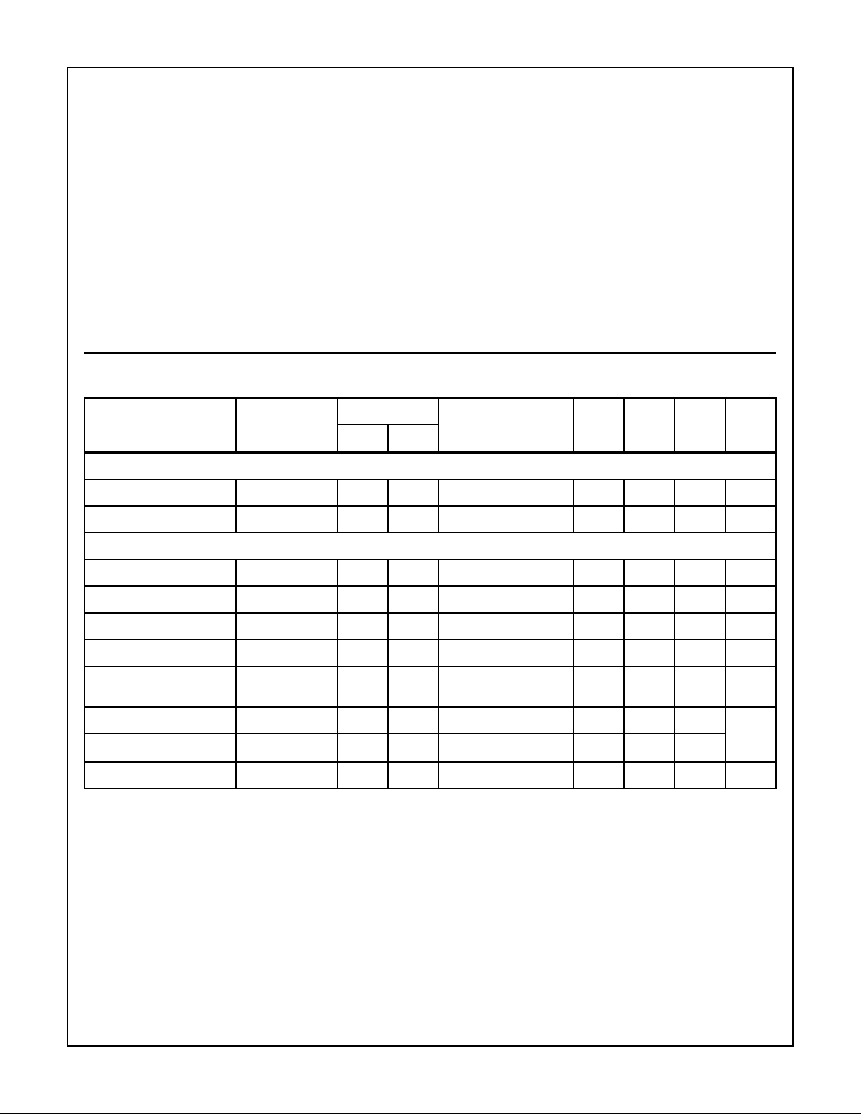
Electrical Specifications T
= 25oC, Chroma Gain Control at maximum position for all tests except as noted. Electrical
A
specifications referenced to test circuit.
TERMINAL,
SWITCH POS.
MEASUREMENT
PARAMETER
AND SYMBOL
1
S
V
2
CHROMA
INPUT TP
MIN TYP MAX
1
DC ELECTRICAL SPECIFICATIONS
Voltage Regulator V
Supply Current I
12
12
2 2 0 10.1 11.2 12.1 V
2 2 0 162538mA
SWITCHING ELECTRICAL SPECIFICATIONS (Note 3)
Pull-In Range (Note 4) V
Oscillator Output V
100% Chroma Output V
Overload Detector V
Minimum Chroma Output
8
8
15
15
V
15
(Note 6) 2 0.5V
P-P
±250 - - Hz
2 2 0 0.6 1.0 - V
1 2 0.5V
1 1 0.5V
1 2 0.5V
P-P
P-P
P-P
1.4 2.7 - V
0.4 - 0.7 V
- - 20 mV
(Note 5)
200% Chroma Output V
20% Chroma Output V
Kill Level V
15
15
TP1
12 1V
1 2 0.1V
P-P
P-P
70 100 140 % of
40 - 105
1 2 Vary 5 - 60 mV
NOTES:
3. Except for pull-in range testing, tune oscillator trimmer capacitor for free running frequency of 3.579545MHz±10Hz.
4. Set Switch 1 to Position 2, detune oscillator±250Hz, set Switch 1 to Position 1, and check for oscillator pull-in.
5. Set Chroma Gain Control to minimum position (CCW).
UNITSS
P-P
P-P
P-P
P-P
100%
Reading
P-P
8-34
Page 3

Test Circuit
CA3126
+24V
CW
10kΩ
CCW
CHROMA
GAIN
CONTROL
V
REG
47kΩ
1µF
0.01µF
TP
CHROMA
INPUT
SIGNAL
10kΩ
3.9kΩ
16 15 14 13
1 2 3 4 5 6 7 8
2
kΩ
2.45kΩ
1
S
1
1
0.1µF
0.01µF 0.01µF 0.01µF
2
50Ω
270Ω
2N2102
1
2
S
2
0.01µF
12 11 10 9
CA3126
VARIABLE
ATTENUATOR
0.05µF
I
XTAL
3.579545MHz
0.02µF 0.02µF
1µF
680Ω
10pF
NPO
TEST SIGNAL
GENERATOR
20pF
N750
0.01µF
33pF
N750
BURST
SYNC.
OSCILLOSCOPE
2kΩ
COUNTER
SUBCARRIER
OUTPUT
KEY
PULSE
PULSE
GENERATOR
Pin numbers refer to the PDIP package.
(A) Chroma input signal
(B) Key pulse input signal
(A)
(B)
2.5µs
BURST
63.5µs
3.579545MHz
4µs
5µs CENTERED ON BURST
0.46V
1.0V
V
CHROMA
PEAK
CHROMA
(MIN)
8-35
Page 4

Block Diagram
CA3126
TV CHROMA PROCESSOR
TO
TERM. 12
CW
CHROMA GAIN
10
kΩ
CCW
CHROMA
INPUT
CONTROL
50kΩ
1.2kΩ
2.45kΩ
0.01µF
CHROMA
KILLER
FILTER
GND
INPUT
1
16
2µF
5
BYPASS
0.01µF
FIRST
CHROMA
AMPL.
ACC
AMPL.
RF
AFPC
FILTER
1.0µF
0.01µF
4 3 6
SIGNAL
SAMPLE
AFPC
DET.
-π/4
φ SHIFTER
+π/4
φ SHIFTER
ACC
DET.
AND HOLD
BIAS
SAMPLE
AND HOLD
INTERN.
REF.
ATTENU-
ATOR
BIAS
CONTROL
SIGNAL
SAMPLE
AND HOLD
BIAS
SAMPLE
AND HOLD
2kΩ
2
0.01µF
680Ω
DC CONTR.
BALANCED
φ SHIFTER
OVERLOAD
DETECTOR
SECOND
CHROMA
AMPL.
BALANCE-
UNBALANCE
TRANSLATOR
CRYSTAL
FILTER
20pF
10pF
VCO
AMPL.
LIMIT
COUPLING
NETWORK
KILLER
AMPL.
DELA Y
BIAS
33pF
7
CARRIER
OUTPUT
SUPPLY
AMPL.
+11.2V
ZENER
REF.
KEYER
8
13
12
15
14
9
0.01µF
0.05
µF
3.9kΩ
2kΩ
2N2102
(NOTE 6)
0.01
µF
(NOTE 6)
VOLTAGE
270Ω 10kΩ
CHROMA
OUTPUT
5µs WIDTH
HORIZONTAL
KEY INPUT
+24V
0V
CA3126
NOTES:
6. Optional design features.
7. Pinout numbers refer to the PDIP package.
10 11
0.01µF 0.01µF
1µF
ACC
FILTER
8-36
DELA Y
BIAS
Page 5
Schematic Diagram
CA3126
RF BYPASS
4
1
CHROMA
INPUT
CHROMA
OUTPUT
15
R
1.5K
60
FIRST CHROMA
AMPLIFIER
R
1
300
R
2
700
Q
Q
1
R
6
Q
3
500
R
3
250
2.2K
SECOND CHROMA
AMPLIFIER
R
43
2.5K
Q
65
Q
Q
66
R
300
R
700
Q
23
A
B
C
D
E
F
G
H
I
J
K
L
M
N
Q
53
R
15
700
R
16
12K
R
12K
R
54
4K
Q
36
SINGLE SAMPLE
AND HOLD
R
17
2K
Q
11
Q
19
R
18
1K
SIGNAL SAMPLE
Q
72
R
Q
54
5K
Q
12
13
AND HOLD
R
57
2K
R
59
2K
20
AFPC DETECTOR
R
13
Q
71
Q
Q51Q
9
4
5
Q
50
R
2
7
R
11
1.3K
C
3
5pF
Q
7
4K
Q
Q
R
2.1K
8
10
14
C
10pF
1
52
500
R
10
1.6K
R
R
8
500
D
9
1
Q
5
Q
6
Q
4
R
12
1K
ACC
DETECTOR
1K
Q
68
80
78
Q
Q
69
35
Q
33
Q
70
Q
34
Q
24
R
O
Q
32
Q
31
P
CHROMA
GAIN
CONTROL
16
13
OVERLOAD
DETECTOR
R
300
79
Q
22
Q
Q
R
8K
R
1K
R
330
D
67
42
25
41
40
3
R
R
77
750
Q
20
KILLER
AMP.
5K
44
Q
27
ACC
AMP.
R
49
700
Q
29
R
46
5K
R
48
2K
Q
28
R
47
5K
R
45
220
R
2K
R
5K
51
50
OVERLOAD DETECTOR
5 14
NOTE: Pin numbers refer to the PDIP Package. Resistance values are in ohms.
8-37
Q
30
R
52
1K
GROUND
(SUBSTRATE)
ZENER
REFERENCE
D
1
Z
2
Z
3
Q
47
R
700
R
3.5K
ZENER
REFERENCE
Q
53
55
R
S
T
Page 6
CA3126
Schematic Diagram
AFPC FILTER XTAL FILTER
2 3 6 7
A
B
C
D
E
F
G
H
I
J
K
L
M
N
O
P
PHASE SHIFTER
Q
55
Q
56
R
63
Q
73
100
Q
40
Q
39
BALANCED
Q
R
5K
Q
(Continued)
Q
64
Q
R
22
2K
Q
15
14
21
R
64
4.9K
41
R
24
Q
58
C
2
12pF
R
23
8.2K
TRANSLATOR
R
69
2K
Q
43
5K
D
6
Q
76
57
BALANCE - UNBALANCE
Q
R
56
3.5K
BIAS SAMPLE
AND HOLD
Q
59
Q
Q
17
Q
R
25
1K
37
CARRIER
OUTPUT
8
LIMITER AMPLIFIER
R
27
R
26
2K
18
16
Q
R
71
5K
3K
Q
21
R
28
390
R
430
Q
30
60
R
750
Q
19
32
Q
61
R
29
390
R
3
4K
R
35
4.5K
Q
20
OSCILLATOR
BIAS SAMPLE
79
Q
45
Q
44
Q
Q
81
R
34
1K
R
33
1K
R
36
2.2K
AND HOLD
62
R
36
3K
Q
49
R
37
Q
63
2.2K
R
38
1.5K
R
39
500
D
2
POWER
SUPPLY
12
+V
CC
10
ACC
Q
46
FILTER
11
R
72
2K
R
62
1.8K
Q
R
70
2.4K
75
KEYER
Q
R
1K
R
61
2.94K
Q
38
54
R
68
1.5K
Q
74
R
R
65
67
5K
1.5K
Q
42
R
66
2K
R
S
T
HORIZONTAL
9
KEYING INPUT
Q
77
R
73
2.5K
R
Z
1
74
1K
D
5
D
4
R
1.2K
Q
48
75
VOLTAGE REFERENCES
8-38
Page 7

CA3126
Application Information
Circuit Description (Pin numbers refer to the DIP package.)
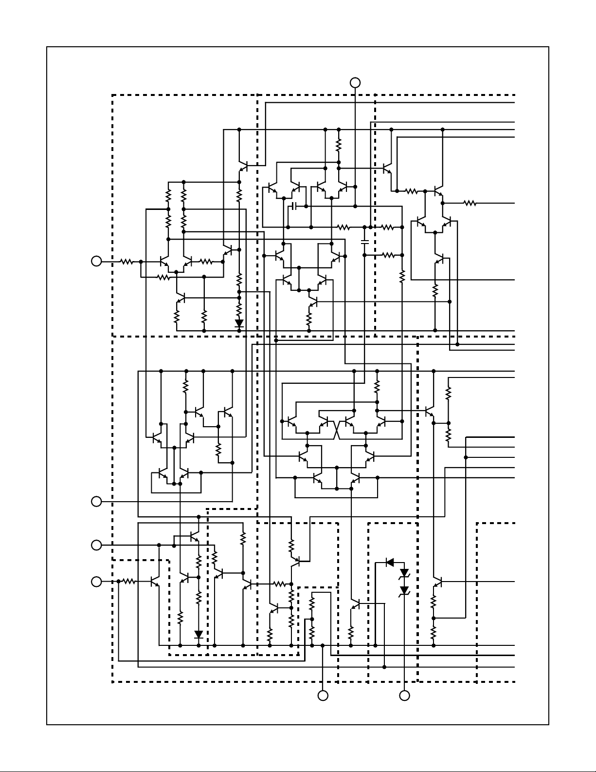
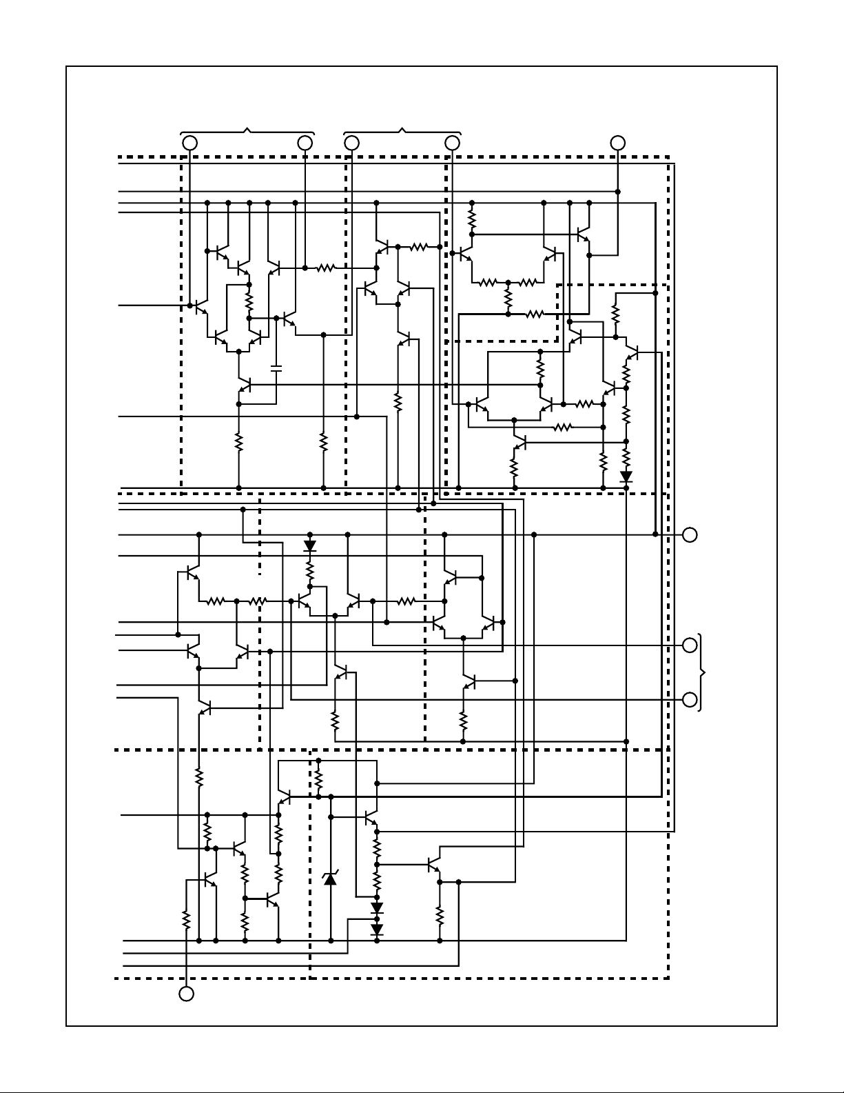
The following paragraphs briefly describe the circuit operation
of the CA3126 (shown in the Block Diagram and Schematic
Diagram). A detailed description of the operation of various
portions of the CA3126 is given in AN6247, “Application of the
CA3126 Chroma-Processing lC Using Sample-and-Hold
Techniques”.
The chroma input is applied to Terminal 1 through the desired
band-shaping network. A 2,450Ω resistor should be placed in
series with Ter minal 1 to minimize oscillator pickup in the first
chroma amplifier. This amplifier supplies signals to the second
chroma amplifier and to the ACC and AFPC detectors. The
first chroma amplifier is gain-controlled by the ACC amplifier.
A horizontal keying pulse is applied to Terminal 9. This pulse
must be present to ensure proper operation of the oscillator circuit. The subcarrier burst is sampled during the keying interval
in the AFPC detector. The error v oltage, produced at Terminal 2
and proportional to the burst phase, is compared to the quiescent bias voltage at Terminal 3 by the sample-and-hold circuitry.
This “compared” voltage controls the phase- shifting network in
the phase-locked loop. The oper ation of the AFPC loop is independent of any external adjustments or voltages except for an
initial capacitor adjustment to set the free-running frequency .
The regenerated oscillator signal at Terminal 8 is applied
internally to the AFPC and ACC detectors through +45 and
-45-degree phase-shifter networks to establish the proper
phase relationship for these detectors. The ACC detector,
which also samples the burst during the keying interval, produces a correction voltage proportional to the burst amplitude. The correction voltage is compared to the quiescent
bias level using sample-and-hold circuitry similar to that
used in the AFPC portion of the circuit. The “compared” voltage is applied internally to the ACC amplifier and killer
amplifier. Because the amplifier gains and killer threshold
are determined by the ratios of the internal resistors, these
functions are independent of external voltages or controls.
The attenuated chroma signal is fed to the second chroma
amplifier, where the burst is removed by keyer action. The
killer amplifier, the chroma gain control, and the overload
detector control the action of the second chroma amplifier,
whose gain is proportional to the dc voltage at Ter minal 16.
The overload detector (Terminal 13) receives a sample of
the chroma output (Ter minal 15) and detects the peak of the
signal. The detected voltage is stored in an external capacitor connected to Ter minal 16. This stored voltage on Terminal 16 affects the gain of the second chroma in the same
manner as the chroma gain control.
General Considerations
The block diagram shown is typical of the type of circuit used
in the practical application of the CA3126. Several items are
critical for proper operation of the circuit.
1. A series resistor of approximately 2,450Ω (or high source
impedance) must be used at the chroma input, Terminal
1. This high impedance minimizes pickup of unbalanced
currents, particularly of the subcarrier oscillator signal.
2. When the overload detector is used, a large resistor
(nominally 47,000Ω) must be placed in series with Ter minal 16 to set the required RC time constant. The same
RC network series serves to set the killer time constant.
3. The setting of the free-running oscillator frequency
requires the presence of the keying pulse. The free-running frequency will be erroneous if Terminal 1 is DC
shorted during the setting operation because of the DC
offset voltage introduced to the AFPC detector.
4. Care must be taken in PC board designs to provide reasonable isolation between the oscillator portion of the circuit
(Terminals 6, 7, and 8) and the chroma input (Terminal 1).
Overload Detector
The overload detector accomplishes two purposes:
1. It prevents oversatur ation due to low b urst-to-chroma r atios.
2. It prevents overload conditions due to noise.
Both of these conditions are discussed in more detail in
AN6247. The extent to which the overload detector is used
depends upon the individual receiver design goals. If greater
than 0.5V
output is desired, the chroma output at Ter mi-
P-P
nal 15 can be tapped to yield any desired degree of overload
detector action.
Chroma Gain Control
The chroma gain control operates by varying the base bias on
current source transistor Q
. To ensure proper temperature
25
tracking of the chroma gain control, it is essential that the control be operated from a supply source derived from the reference voltage at Terminal 12. Because the control operates from
a current source, chroma gain is much more predictable and far
less temperature sensitive than controls that steer current by
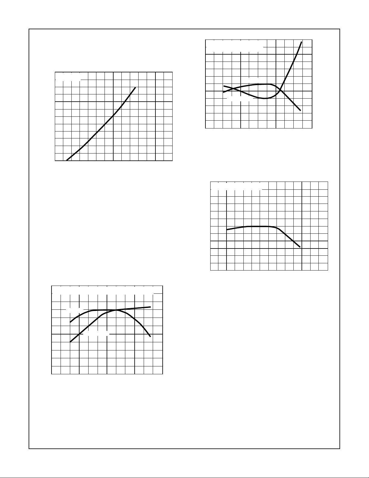
means of a differential amplifier. The typical chroma gain characteristic for the CA3126 is shown in Figure 1.
TA = 25oC, CHROMA INPUT = 0.5V
100
80
60
40
20
CHROMA OUTPUT (% OF MAX. VALUE)
VOLTAGE AT TERMINAL 16 (% OF V12)
FIGURE 1. CHROMA GAIN CONTROL
P-P
120020406080100
140
Subcarrier Regenerator Oscillator
The oscillator filter consists of a 3.579545MHz crystal, a 680Ω
resistor, and a 10pF capacitor connected in series across Terminals 6 and 7. A 33pF capacitor, shunt connected from Terminal 7 to ground, rolls off higher order harmonics, thereby
preventing oscillation at the crystal third-harmonic frequency. A
8-39
Page 8
CA3126
curve of the typical static phase error as a function of the freerunning oscillator frequency is shown in Figure 2. It should be
noted that the slope of the curve determines the DC gain of the
phase-locked loop, i.e ., 40Hz per deg ree.
TA = 25oC
6
4
2
0
-2
STATIC PHASE ERROR (DEGREES)
-4
400
300-300 -200 -100 0 100 200
OSCILLATOR FREE-RUNNING FREQUENCY
(DEVIATION IN Hz FROM 3.579545MHz)
FIGURE 2. STATIC PHASE ERROR
Thermal Considerations
The circuit of the CA3126 is thermally compensated to achieve
the optimal operating characteristics over the normal operating
temperature range of TV receivers. Figures 3 and 4 show the
oscillator and chroma-output amplitudes and phases as a function of temperature (Terminals 8 and 15), respectively.
Both the oscillator and chroma-output amplitudes and
phases are measured relative to the chroma-input phase.
The performance of the oscillator free-running frequency as
a function of temperature is shown in Figure 5. All the temperature plots are characteristic of the test circuit with the
indicated component types and values given.
CHROMA INPUT = 0.25V
110
C VALUE)
o
100
PHASE
, 3.58MHz CW SIGNAL
P-P
0
140
CHROMA INPUT = 0.25V
3.58MHz CW SIGNAL
130
C VALUE)
o
120
110
100
90
80
CHROMA OUTPUT AMPLITUDE (% OF 25
AMPLITUDE
TEMPERATURE (oC)
P-P
PHASE
,
FIGURE 4. AMPLITUDE AND PHASE VARIATIONS OF
CHROMA OUTPUT vs TEMPERATURE
CHROMA INPUT = 0V
100
50
0
-50
-100
(DEVIATION IN Hz FROM 3.579545 MHz)
OSCILLATOR FREE-RUNNING FREQUENCY
-150
P-P
TEMPERATURE (oC)
FIGURE 5. VARIATION OF OSCILLATOR FREE RUNNING
C VALUE)
o
FREQUENCY vs TEMPERATURE
15
10
5
0
-5
CHROMA OUTPUT PHASE
-10
-15
100-50 -25 0 25 50 75
125-50 -25 0 25 50 75
100
C VALUE)
o
(DEGREE OF DEVIATION FR OM 25
90
AMPLITUDE
80
70
60
OSCILLATOR AMPLITUDE (% OF 25
TEMPERATURE (oC)
FIGURE 3. AMPLITUDE AND PHASE VARIATIONS OF
OSCILLATOR OUTPUT vs TEMPERATURE
100-50 -25 0 25 50 75
-5
-10
OSCILLATOR PHASE
(DEGREE OF DEVIATION FROM 25
8-40
Page 9
INPUT FILTER
68pF
L2
27µH
TYP. 0.5V
56
pF
82pF
L1
12µH
COMPOSITE
VIDEO/CHROMA INPUT
P-P
500Ω
2.4kΩ
0.01µF
1
+12V
0.01µF
12
V
CC
CA3126
CHROMA
FIRST
AMP
CA3126
0.01µF
0.01µF
0.01µF
1µF
2kΩ
43
DET/FILT.
BURST-GATE
2
AFPC
CHROMA/
SWITCH
6
680Ω
VCO
XTAL
2ND
CHROMA
AMP
5pF-25pF
10pF
7
SUBCARRIER
AMP
33pF
FSC
3.579545MHz
SUBCARRIER
OUTPUT (CW)
8
0.01µF
15
ACC
AMP
11.2V
ZENER
REF
14
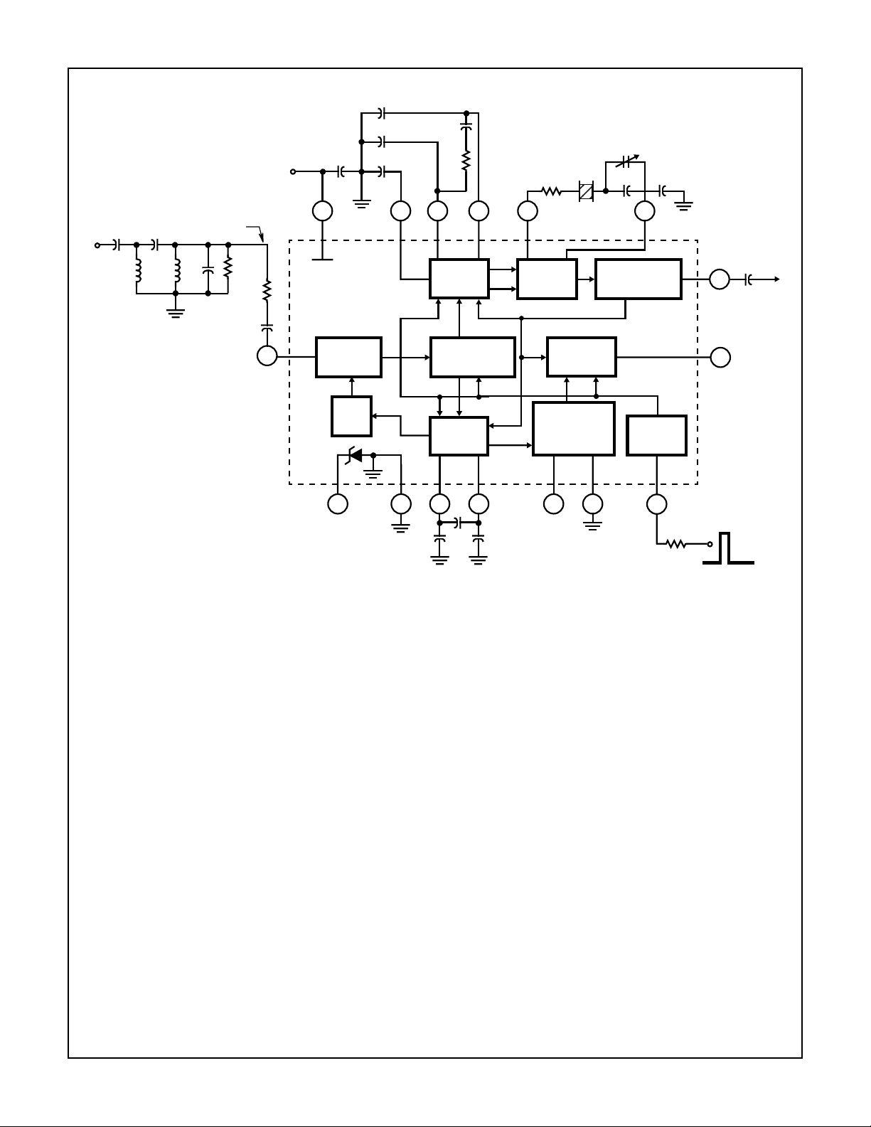
NOTE: For Subcarrier Regenerator, the second chroma
amp is not used; Pins 13,14, and 15 are not connected and
pin 16 is grounded.
FIGURE 6. TYPICAL APPLICATION OF THE CA3126 AS A SUBCARRIER REGENERATOR
5
0.01µF
ACC
DET/FILT.
10
1µF
11
0.01µF
CHROMA
O.L. DET
KILLER AND
GAIN CONT.
13
16
BURST
KEYER
AMP
9
2kΩ
BURST KEY PULSE
4µs (TYP), CENTERED
ON BURST
>1V
PEAK
0V
8-41
 Loading...