

Page 1
CA16-Type 2.5 Gbits/s DWDM Transponder with
16-Channel 155 Mbits/s Multiplexer/Demultiplexer
Multiple alarms:
■
— Loss of signal.
— Loss of reference clock.
— Loss of framing.
— Laser degrade alarm.
Applications
Telecommunications:
■
— Inter- and intraoffice SONET/SDH
— Subscriber loop
— Metropolitan area networks
Advance Data Sheet
March 2001
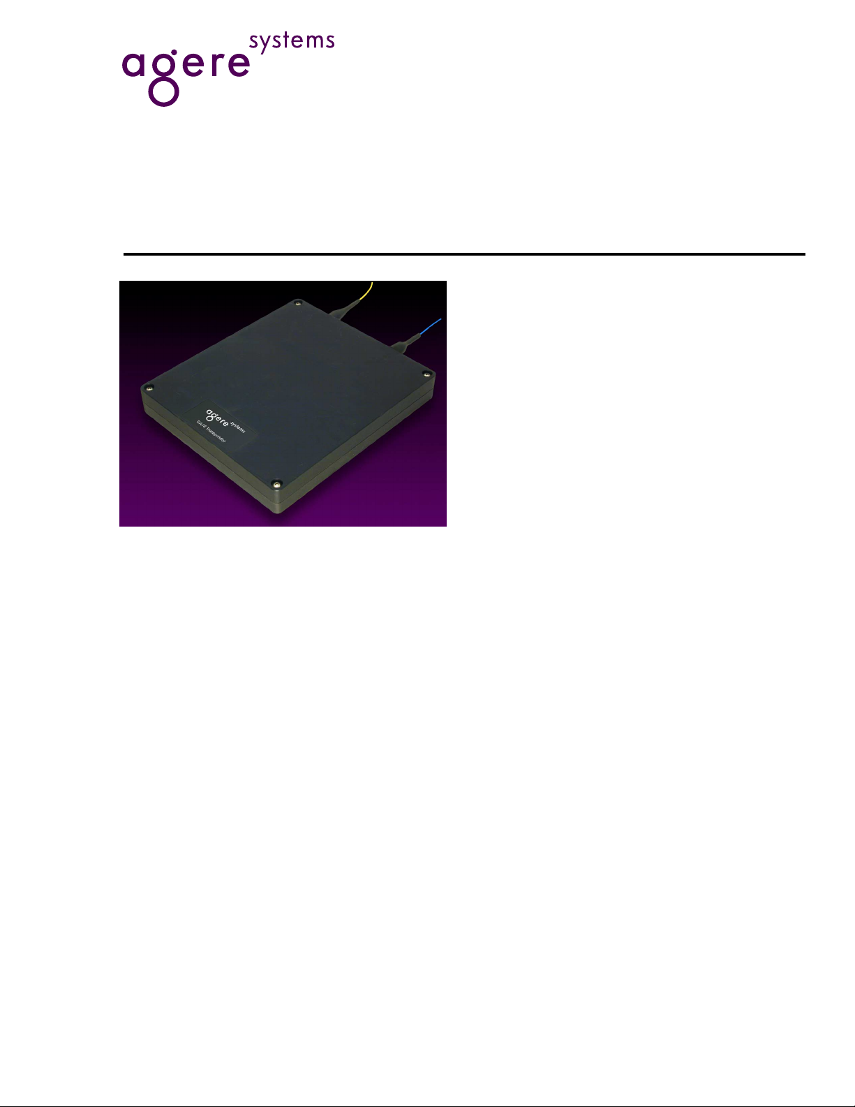
The CA16-type transponder s integrate up to 15 discre te
ICs and optical components, including a 2.5Gbits/s op-
tical transmitter and receiver pair, all in a single, compact packag e.
Features
2.5 Gbits/s optical transmitter and receiver with
■
16-channel 155 Mbits/s multiplexer/demultiplexer.
Available with 1.55 µm cooled DFB laser transmit-
■
ter and an APD receiver for long-reach applications:
— Offers 45 standard ITU wavelengths with
100 GHz spacing.
— Each module is capable of two wavelengths
under user control.
Pig ta iled, low- p r o file pack age.
■
Differential LVPECL data interface.
■
Operating case temperature range: 0 °C to 65 °C.
■
Automatic transmitter optical power control.
■
High-speed data communications
■
Description
The CA16-type transponder performs the parallel-toserial-to-optical transport and optical transport-toserial-to-parallel function of the section and photonic
layers of the SONET/SDH protocol. The CA16 transmitter se ctio n performs the bit ser i al i z a ti o n and op tical transmission of SONET/SDH OC-48/STM-16
data that has been formatted into standard SONET/
SDH compliant 16-bit parallel format. The CA16
receiver performs the optical-to-electrical conversion
function and is then able to detect frame and byte
boundaries and demultiplex the serial data into 16-bit
parallel OC-48/STM-16 format.
The CA16 transponder does not perform byte-level
multiplexing or interleaving.
Laser bias monitor outp ut.
■
Trans mitter laser disable input.
■
Line loopback and diagnostic loopback capability.
■
Page 2

CA16-Type 2.5 Gbits/s DWDM Transponder with Advance Data Sheet
16-Chann el 155 Mb its/s Mu ltip lexer/Demu ltip le x er March 2001
Table of Contents
Contents Page Tables Page
Features ................................................................... 1
Applications .............................................................. 1
Description ............................................................... 1
Absolute Maximum Ratings...................................... 3
Block Diagram........................................................... 4
Pin Information ......................................................... 5
Pin Descriptions....................................................... 6
Functional Description .......... ................................. 12
Receiver ............................................................ 12
Transmitter ........................................................ 12
Loopback Modes............................................... 13
Transponder Interfacing..................................... 13
Optical Charac te r i stics ............................. ............ ..15
Electrical Characteristics ........................................ 16
Timing Characteristics........................................... 18
Transmitter Data Input Timing ........................... 18
Input Timing Mode 1 .......................................... 19
Input Timing Mode 2 .......................................... 20
Forward Clocking ...............................................21
PC
-to PICLK Timing........................................ 22
LK
PHERR/PHINIT.................................................. 2 3
Receiver Framing...............................................25
Wavelength Selection ............................................. 26
Qualification and Reliability .................................... 27
Laser Safety Information ....................................... 27
Class I Laser Product......................................... 27
Electromagnetic Em iss ions and Immunit y.......... 27
Outline Diagram ..................................................... 28
Ordering Information .............................................. 29
Related Product Information................................... 29
Table 1. CA16-Type Transponder Pinout .................6
Table 2. CA16-Type Transponder Input Pin
Descriptions...............................................10
Table 3. CA16-Type Transponder Output Pin
Descriptions ...............................................11
Table 4. OC-48/STM-1 6 Transmitter Optical
Characteristics .......................................... 15
Table 5. OC-48/STM-16 Receiver Optical
Characteristics .......................................... 15
Table 6. Power Supply Characteristics....................16
Table 7. Transmitter Electrical I/O Characteristics...16
Table 8. Receiver Electrical I/O Characteristics ......17
Table 9. Transmitter ac Timing Characteristics .......24
Table 10. Receiver ac Timing Characteristics .........24
Table 11. Ordering Information................................29
Table 12. Related Product Information ....................29
Figures Page
Figure 1. CA16-Type Tra nsponder Block Diagram ....4
Figure 2. CA16-Type Transponder Pinout.................5
Figure 3. Transponder Interfacing............................13
Figure 4. Interfacing to the T
Figure 5. Block Diagram Timing Mode 1..................19
Figure 6. Block Diagram Timing Mode 2..................20
Figure 7. Forward Clocking of the
CA16 Transponder ..................................21
Figure 8. PC
Figure 9. PHERR/PHINIT Timing. ........... .................23
Figure 10. ac Input Timing .......................................24
Figure 11. Receiver Output Timing Diagram ...........24
Figure 12. Frame and Byte Detection......................25
Figure 13. OOF Timing (FRAMEN = High)............ ..25
Figure 14. FRAME N Tim ing.................... ............ .....26
-to PICLK Timing...............................22
LK
XREFCLK
Input.............14
2
Agere Systems Inc..
Page 3

Advance Data Sheet CA16-Type 2.5 Gbits/s DWDM Transponder with
March 2001 16-Channel 155 Mbits/s Multiplexer/Demultiplexer
Description
(continued)
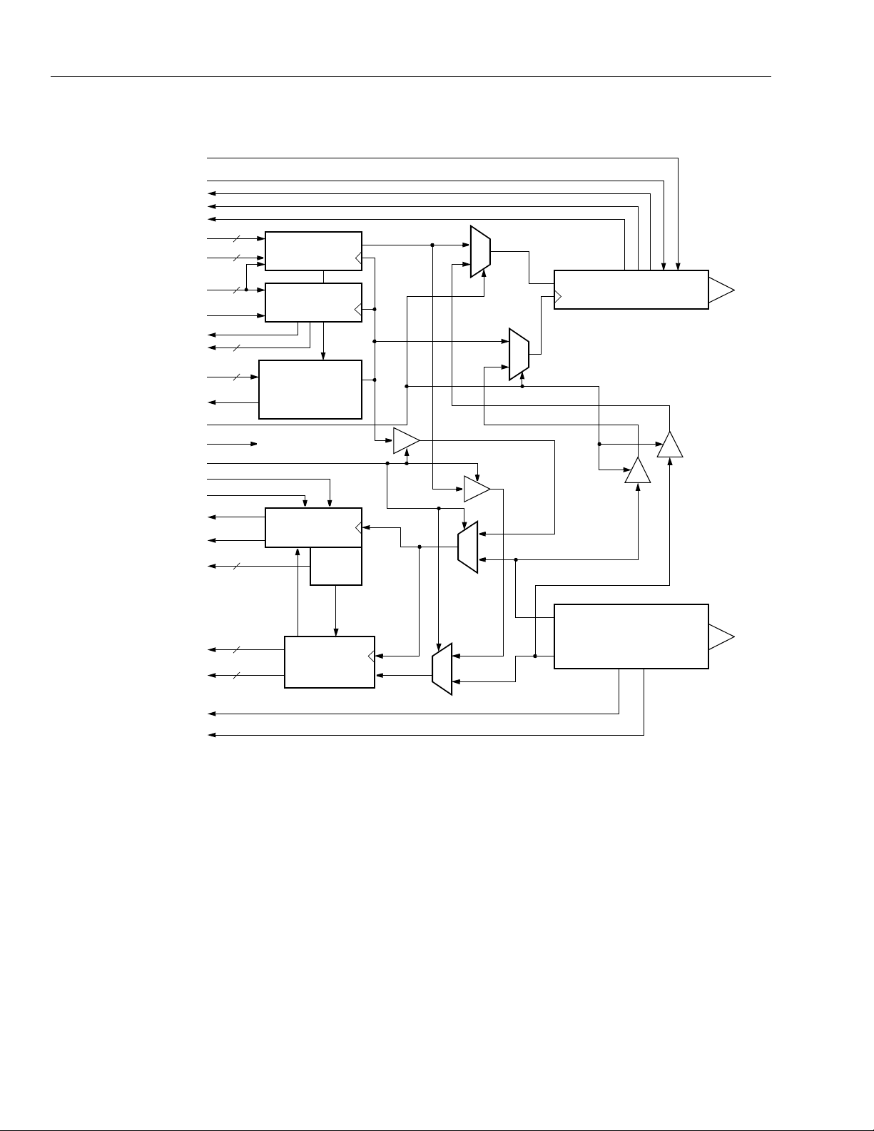
Figure 1 shows a simplified block diagram of the CA16Type transponder. This device is a bidirectional module
designed to provide a SONET or S DH compliant electro-optical interface between the SONET/SDH photonic
physical layer and the electrical section layer. The module contains a wavelength-tunable (two channels at
100 GHz) 2.5 Gbits/s optical transmitter and a
2.5 Gbits/s optical receiver in the same physical package along with the electronics necessary to multiplex
and demultiplex sixteen 155 Mbits/s electrical channels.
Clock synthesis, clock recovery , and SONET/SDH
frame detection ci rcuits are also included within the
module.
In the transmit direction, the transponder module multiplexes sixteen 155 Mbits/s PECL electrical data signals
into an optical signal at 2488.32 Mbits/s for launching
into optical fiber. An internal 2.488 GHz reference oscillator is phase-locked to an external 155.52 MHz data
timing refe rence.
Absolute Maximum Ratings
The optical transmitter is available at any ITU grid
wavelength with a 1.55 µm cooled DFB laser for longreach applications. Th e optical outp u t signal is S ONET
and ITU compliant for OC-48/STM-16 applications as
shown in Table 4, OC-48/STM-1 6 Transmitter Optical
Characteristics.
In the receive direction, the transponder module
receives a 2488.32 Mbits/s optical signal and converts
it to an electrical signal, and then extracts a clock signal and demultiplexes the data into sixteen 155 Mbits/s
differential LV PECL data signals. When enabled, the
module can also detect SONET/SDH frame boundaries. The optical receiver is available with an APD
photodetector. The receiver operates over the wavelength range of 1.1 µm to 1.6 µm and is fully com pliant
to SONET/SDH OC-48/STM-16 physical layer specifications as shown in Table 5, OC-48/STM-16 Receiver
Optical Characteristics.
Stresses in excess of the absol ute maximum ratings can cause permanent damage to the dev ice. These are absolute stress ratin gs onl y. Function al operatio n of the device is not implied at thes e or any o ther conditions in excess
of those given in the operations sections of the data sheet. Exposure to absolute maximum ratings for extended
periods can adversely affect reliability.
Parameter Symbol Min Max Unit
Operating Case Temperature Range T
Storage Case Temperature Range T
C
S
075°C
–40 85 °C
Supply Voltage — –0.5 5.5 V
Voltage o n Any LV PECL P in — 0 V
CC
—
High-speed LVPECL Output Source Current — — 50 mA
Static Discharge Voltage
1
ESD — 500 V
Relative Humidity (noncondensing) RH — 85 %
Receiver Optical Input Power—Biased APD P
IN
—0dBm
Minimum Fiber Bend Radius — 1.25 (31.8) — in. (mm)
1. Human body model.
Agere Systems Inc.
3
Page 4
CA16-Type 2.5 Gbits/s DWDM Transponder with Advance Data Sheet
16-Chann el 155 Mb its/s Mu ltip lexer/Demu ltip le x er March 2001
Block Diagram
WS (WAVELENGTH
SELECT)
TXDIS
WDEA
LSR ALRM
LPM
TXD[0:15]P
TXD[0:15]N
PICLKP/N
PHINIT
PHERR
PCLKP/N
TXREFCLKP/N
LOCKDET
LLOOP
RESET
DLOOP
OOF
FRAMEN
SEARCH
FP
POCLKP/N
16
16
2
2
2
CLOCK DIVIDER
PHASE DETECT
2
16:1 PARALLEL
TO SERIAL
TIMING
GENERATION
AND
FRAME/BYTE
DETECT
TIMING
GEN
MUX
D
OC-48/STM-16
OPTICAL TRANSMITTER
MUX
MUX
RXQ[0:15]P
RXQ[0:15]N
LOS
IPDMON
16
16
1:16 SERIAL
TO PARALLEL
MUX
Figure 1. CA16-Type Transponder Block Diagram
CK
OC-48/STM-16
OPTICAL RECEIVER
W/CLOCK RECOVERY
D
1-1011(F).f
4
Agere Systems Inc.
Page 5
Advance Data Sheet CA16-Type 2.5 Gbits/s DWDM Transponder with
March 2001 16-Channel 155 Mbits/s Multiplexer/Demultiplexer
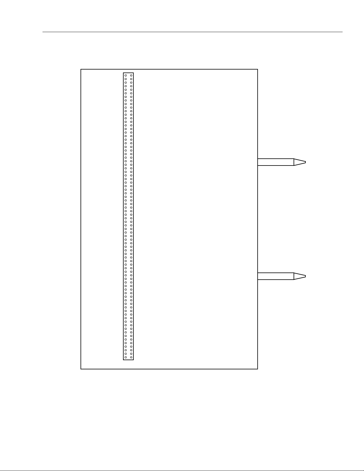
Pin Information
60
50
40
30
20
10
1
FGND
NC
NC
NC
NC
RXDGND
RXQ00N
RXQ00P
RXQ02N
RXQ02P
RXDGND
RXQ04N
RXQ04P
RXQ06N
RXQ06P
RXDGND
RXQ08N
RXQ08P
RXQ10N
RXQ10P
RXDGND
RXQ12N
RXQ12P
RXQ14N
RXQ14P
RXDGND
VTEC
VTEC
VTEC
RXDGND
RXAGND
RXAGND
RX3.3A
RXAGND
RXAGND
NC
RX3.3D
RX3.3D
RXDGND
FRAMEN
WDEA
DLOOP
NC
LSRBIAS
LSRALM
LPM
TXAGND
TX3.3A
TX3.3A
TXAGND
TX3.3D
TX3.3D
TXDGND
LOCKDET
PICLKN
PICLKP
TXDGND
TXD01N
TXD01P
TXD03N
TXD03P
TXDGND
TXD05N
TXD05P
TXD07N
TXD07P
TXDGND
TXD09N
TXD09P
TXD11N
TXD11P
TXDGND
TXD13N
TXD13P
TXD15N
TXD15P
TXDGND
IPDMON
FGND
FGND 16080
NC
NC
NC
NC
RXDGND
RXQ01N
RXQ01P
RXQ03N
RXQ03P
RXDGND 15070
RXQ05N
RXQ05P
RXQ07N
RXQ07P
RXDGND
RXQ09N
RXQ09P
RXQ11N
RXQ11P
RXDGND 140
RXQ13N
RXQ13P
RXQ15N
RXQ15P
RXDGND
VTEC
VTEC
WS
NC
POCLKN
POCLKP
RX3.3A
RXAGND
RXAGND
SEARCH
RX3.3D
RX3.3D
RXDGND
OOF
FP
RXDGND
LOS
LLOOP
PHERR
NC
TXDIS
PHINIT
NC
TX3.3A
TX3.3D
TXAGND
TXDGND
PCLKN
PCLKP
TXDGND
TXD00N
TXD00P
TXDGND
TXD02N
TXD02P
TXD04N
TXD04P
TXDGND
TXD06N
TXD06P
TXD08N
TXD08P
TXDGND
TXD10N
TXD10P
TXD12N
TXD12P
TXDGND
TXD14N
TXD14P
TXREFCLKN
TXREFCLKP
TXDGND
RESET
FGND
130
120
110
100
90
81
RX
TX
TOP VIEW
Agere Systems Inc.
1-1014(F).d
Figure 2. CA16-Type Transponder Pinout
5
Page 6

CA16-Type 2.5 Gbits/s DWDM Transponder with Advance Data Sheet
16-Chann el 155 Mb its/s Mu ltip lexer/Demu ltip le x er March 2001
Pin Descriptions
Table 1. CA16-Type Transponder Pinout
Pin # Pin Name I/O Logic Description
01 FGND I Supply Frame Ground
02 IPDMON O Analog Receiver Photodiode Curren t Monitor
03 TxDGND I Supply Transmitter Digital Ground
04 TxD15P I LVPECL Trans mi tter 155 Mbits/s MSB Data Input
05 TxD15N I LVPECL Transmitter 155 Mbits/s MSB Data Input
06 TxD13P I LVPECL Transmitter 155 Mbits/s Data Input
07 TxD13N I LVPECL Transmitter 155 Mbits/s Data Input
08 TxDGND I Supply Transmitter Digital Ground
09 TxD11P I LVPECL Transmitter 155 Mbits/s Data Input
10 TxD11N I LVPECL Transmitter 155 Mbits/s Data Input
11 TxD09P I LVPECL Transmitter 155 Mbits/s Data Input
12 TxD09N I LVPECL Transmitter 155 Mbits/s Data Input
13 TxDGND I SUPPLY Transmitter Digital Ground
14 TxD07P I LVPECL Transmitter 155 Mbits/s Data Input
15 TxD07N I LVPECL Transmitter 155 Mbits/s Data Input
16 TxD05P I LVPECL Transmitter 155 Mbits/s Data Input
17 TxD05N I LVPECL Transmitter 155 Mbits/s Data Input
18 TxDGND I Supply Transmitter Digital Ground
19 TxD03P I LVPECL Transmitter 155 Mbits/s Data Input
20 TxD03N I LVPECL Transmitter 155 Mbits/s Data Input
21 TxD01P I LVPECL Transmitter 155 Mbits/s Data Input
22 TxD01N I LVPECL Transmitter 155 Mbits/s Data Input
23 TxDGND I Supply Transmitter Digital Ground
24 PIC
25 PIC
P I LVPECL Byte-Aligned Parallel Input Clock at 155 MHz
LK
N I LVPECL Byte-Aligned Parallel Input Clock at 155 MHz
LK
26 LOCKDET O LVTTL Lock Detect
27 TxDGND I Supply Transmitter Digital Ground
28 Tx3. 3D I Supply Trans mi tter 3.3 V Digital Supply
29 Tx3. 3D I Supply Trans mi tter 3.3 V Digital Supply
30 TxAGND I Supply Transmitter Analog Ground
31 Tx3.3A I Supply Transmitter 3.3 V Analog Supply
32 Tx3.3A I Supply Transmitter 3.3 V Analog Supply
33 TxAGND I Supply Transmitter Analog Ground
34 LPM O Analog Laser Power Monitor
35 LSRALM O 5 V CMOS Laser Degrade Alarm
36 LSRBIAS O Analog Not Implemented on the CA16-Type Transponder
37 NC — — No User Connection Permitted
38 D
LOOP
I LVTTL Diagnostic Loopback
39 WDEA O 5 V CMOS Wavelength Deviation Error Alarm
40 FP O LVPECL Frame Pulse
41 FRAMEN I LVTTL Frame Enable
1. Frame ground is connected to the housing and is isolated from all circu it grounds (TxDGND, TxAGND, RxDGND, RxAGND).
2. Pins labeled no connec t i on must rem ain open c i rc uits; they have internal voltages and must not be con nected to V
or any signal node.
1
2
CC
, Grou nd,
6
Agere Systems Inc.
Page 7

Advance Data Sheet CA16-Type 2.5 Gbits/s DWDM Transponder with
March 2001 16-Channel 155 Mbits/s Multiplexer/Demultiplexer
Pin Descriptions
(continued)
Table 1. CA16-Type Transponder Pinout (continued)
Pin # Pin Name I/O Logic Description
42 RxDGND I Supply Receiver Digital Ground
43 Rx3.3D I Supply Receiver 3.3 V Digital Supply
44 Rx3.3D I Supply Receiver 3.3 V Digital Supply
45 NC — — No User Connection Permitted
2
46 RxAGND I Supply Receiver Analog Ground
47 RxAGND I Supply Receiver Analog Ground
48 Rx3.3A I Supply Receiver 3.3 V Analog Supply
49 RxAGND I Supply Receiver Analog Ground
50 RxAGND I Supply Receiver Analog Ground
51 RxDGND I Supply Receiver Digital Ground
52 VTEC I Supply TEC Cooler 3 V Anal og Supply V ol ta ge
53 VTEC I Supply TEC Cooler 3 V Anal og Supply V ol ta ge
54 VTEC I Supply TEC Cooler 3 V Anal og Supply V ol ta ge
55 RxDGND I Supply Receiver Digital Ground
56 RxQ14P O LV PECL Receiver 155 M b i ts/s Data Output
57 RxQ14N O LVPECL Receiver 155 Mbits/s Data Output
58 RxQ12P O LV PECL Receiver 155 M b i ts/s Data Output
59 RxQ12N O LVPECL Receiver 155 Mbits/s Data Output
60 RxDGND I Supply Receiver Digital Ground
61 RxQ10P O LV PECL Receiver 155 M b i ts/s Data Output
62 RxQ10N O LVPECL Receiver 155 Mbits/s Data Output
63 RxQ08P O LV PECL Receiver 155 M b i ts/s Data Output
64 RxQ08N O LVPECL Receiver 155 Mbits/s Data Output
65 RxDGND I SUPPLY Receiver Digital Ground
66 RxQ06P O LV PECL Receiver 155 M b i ts/s Data Output
67 RxQ06N O LVPECL Receiver 155 Mbits/s Data Output
68 RxQ04P O LV PECL Receiver 155 M b i ts/s Data Output
69 RxQ04N O LVPECL Receiver 155 Mbits/s Data Output
70 RxDGND I Supply Receiver Digital Ground
71 RxQ02P O LV PECL Receiver 155 M b i ts/s Data Output
72 RxQ02N O LVPECL Receiver 155 Mbits/s Data Output
73 RxQ00P O LVPECL Receiver 155 Mbits/s LSB Data Output
74 RxQ00N O LVPECL Receiver 155 Mbits/s LSB Data Output
75 RxDGND I Supply Receiver Digital Ground
76 NC — — No User Connection Permitted
77 NC — — No User Connection Permitted
78 NC — — No User Connection Permitted
79 NC — — No User Connection Permitted
80 FGND I Supply Frame Ground
81 FGND I Supply Frame Ground
1
1
2
2
2
2
82 Reset I — Master Reset
1. Frame ground is connected to the housing and is isolated from all circuit grounds (TxDGND, TxAGND, RxDGND, RxAGND).
2. Pin s lab eled no c onnection must remain open circuits; they have internal voltages and must not be connected to V
or any signal node.
CC
, Grou nd,
Agere Systems Inc.
7
Page 8

CA16-Type 2.5 Gbits/s DWDM Transponder with Advance Data Sheet
16-Chann el 155 Mb its/s Mu ltip lexer/Demu ltip le x er March 2001
Pin Descriptions
(continued)
Table 1. CA16-Type Transponder Pinout (continued)
Pin # Pin Name I/O Logic Description
83 TxDGND I Supply Transmitter Digital Ground
84 TxR
85 TxR
P I LVPECL T ransmitter 155 Mbits/s Reference Clock Input
EFCLK
N I LVPECL Transmitter 155 Mbits/s Reference Clock Input
EFCLK
86 TxD14P I LVPECL Transmitter 155 Mbits/s Data Input
87 TxD14N I LVPECL Transmitter 155 Mbits/s Data Input
88 TxDGND I Supply Transmitter Digital Ground
89 TxD12P I LVPECL Transmitter 155 Mbits/s Data Input
90 TxD12N I LVPECL Transmitter 155 Mbits/s Data Input
91 TxD10P I LVPECL Transmitter 155 Mbits/s Data Input
92 TxD10N I LVPECL Transmitter 155 Mbits/s Data Input
93 TxDGND I SUPPLY Transmitter Digital Ground
94 TxD08P I LVPECL Transmitter 155 Mbits/s Data Input
95 TxD08N I LVPECL Transmitter 155 Mbits/s Data Input
96 TxD06P I LVPECL Transmitter 155 Mbits/s Data Input
97 TxD06N I LVPECL Transmitter 155 Mbits/s Data Input
98 TxDGND I Supply Transmitter Digital Ground
99 TxD04P I LVPECL Transmitter 155 Mbits/s Data Input
100 TxD04N I LVPECL Transmitter 155 Mbits/s Data Input
101 TxD02P I LVPECL Transmitter 155 Mbits/s Data Input
102 TxD02N I LVPECL Transmitter 155 Mbits/s Data Input
103 TxDGND I SUPPLY Transmitter Digital Ground
104 TxD00P I LVPECL Transmitter 155 Mbits/s LS B Data Input
105 TxD00N I LVPECL Transmitter 155 Mbits/s LSB Data Input
106 TxDGND I Supp ly Transmitter Digital Ground
107 PC
108 PC
P O LVPECL Transmitter Parallel Reference Clock Output
LK
N I LVPECL Transmitter Parallel Reference Clock Output
LK
109 TxDGND I Supp ly Transmitter Digital Ground
110 TxAGND I Supply Transmitter Analog Ground
111 Tx3.3D I Supply Transmitter Digital 3.3 V Supply
112 Tx3.3A I Supply T r ansmitter Analog 3.3 V Supply
113 NC — — Future Function (I
2
C Clock)
114 PHINIT I LVPECL Phase Initialization
115 T
116 NC — — Future Function (I
DIS I TTL Transmitter Di sable
X
2
C Data)
117 PHERR O L VPECL Phase Error
118 L
LOOP
I LVTTL Line Loopback (active-low)
119 LOS O LVTTL Loss of Sign al
120 RxDGND I Supply Receiver Digital Ground
121 OOF I LVTT L Out of Frame (enable frame detection)
122 RxDGND I Supply Receiver Digital Ground
123 Rx3.3D I Supp ly Receiver Digital 3.3 V Supply
1. Frame ground is connected to the housing and is isolated from al l cir cu it g rounds (TxDGND, TxAGND, RxDGND, RxAGND).
2. Pins labeled no connec t i on must rema in open circui ts; they have internal voltages and must not be con nected to V
or any signal node.
CC
, Grou nd,
8
Agere Systems Inc.
Page 9

Advance Data Sheet CA16-Type 2.5 Gbits/s DWDM Transponder with
March 2001 16-Channel 155 Mbits/s Multiplexer/Demultiplexer
Pin Descriptions
(continued)
Table 1. CA16-Type Transponder Pinout (continued)
Pin # Pin Name I/O Logic Description
124 Rx3.3D I SUPPLY Receiver Digital 3.3 V Supply
125 SE ARCH O LVTTL Frame Search Output
126 RxAGND I Supply Receiver Analog G r ound
127 RxAGND I Supply Receiver Analog G r ound
128 Rx3.3A I Supply Receiver Analog 3.3 V Supply
129 POC
130 POC
131 NC — — No User Connection Permitted
P O LV PECL Byte-Aligned Parallel Output Clock at 155 MHz
LK
N O LVPECL Byte-Aligned Parallel Output Clock at 155 MHz
LK
2
132 WS I L VTTL Binary Input to Select One of Two Grid Wavelengths
133 VTEC I Supply TEC Cooler 3 V Analog Supply Vol tage
134 VTEC I Supply TEC Cooler 3 V Analog Supply Vol tage
135 RxDGND I Supply Receiver Digital Ground
136 RxQ15P O LVPECL Receiver MSB 155 Mbits/s Data Output
137 RxQ15N O LVPECL Receiver MSB 155 Mbits/s Data Output
138 RxQ13P O LVPECL Receiver 155 Mbits/s Data Output
139 RxQ13N O LVPECL Receiver 155 Mbits/s Data Output
140 RxDGND I Supply Receiver Digital Ground
141 RxQ11P O LVPECL Receiver 155 Mbits/s Data Output
142 RxQ11N O LVPECL Receiver 155 Mbits/s Data Output
143 RxQ09P O LVPECL Receiver 155 Mbits/s Data Output
144 RxQ09N O LVPECL Receiver 155 Mbits/s Data Output
145 RxDGND I Supply Receiver Digital Ground
146 RxQ07P O LVPECL Receiver 155 Mbits/s Data Output
147 RxQ07N O LVPECL Receiver 155 Mbits/s Data Output
148 RxQ05P O LVPECL Receiver 155 Mbits/s Data Output
149 RxQ05N O LVPECL Receiver 155 Mbits/s Data Output
150 RxDGND I Supply Receiver Digital Ground
151 RxQ03P O LVPECL Receiver 155 Mbits/s Data Output
152 RxQ03N O LVPECL Receiver 155 Mbits/s Data Output
153 RxQ01P O LVPECL Receiver 155 Mbits/s Data Output
154 RxQ01N O LVPECL Receiver 155 Mbits/s Data Output
155 RxDGND I Supply Receiver Digital Ground
156 NC — — No User Connection Permitted
157 NC — — No User Connection Permitted
158 NC — — No User Connection Permitted
159 NC — — No User Connection Permitted
160 FGND I Supply Frame Ground
1. Frame ground is connected to the housing and is isolated from all circuit grounds (TxDGND, TxAGND, RxDGND, RxAGND).
2. Pins labeled no connection must remain open circuits; they have internal voltages and must not be connected to V
node.
1
2
2
2
2
CC
, Ground, or any signa l
Agere Systems Inc.
9
Page 10

CA16-Type 2.5 Gbits/s DWDM Transponder with Advance Data Sheet
16-Chann el 155 Mb its/s Mu ltip lexer/Demu ltip le x er March 2001
Pin Descriptions
(continued)
Table 2. CA16-Type Transponder Input Pin Descriptions
Pin Name Pin Description
TxD[0:15]P
TxD[0:15]N
PIC
LK
PIC
LK
16-Bit Differential LVPECL Parallel Input Data Bus. TxD15P/N is the most significant bit of the
input word and is the first bit serialized. TxD00P/N is the least significant bit of the input word and
is the last bit serialized. TxD[0:15]P/N is sampled on the rising edge of PIC
P
Differential LVPECL Parallel Input Clock. A 155 MHz nominally 50% duty cycle input clock to
N
which TxD[0:15]P/N is aligned. The rising edge of PICLK trans fers the data on the 16 TxD inputs
LK
.
into the holding register of the parallel-to-serial converter.
TxR
TxR
EFCLK
EFCLK
P
Differential LVPECL Low Jitter 155.520 MHz Input Reference Clock. T his input i s us ed as the
N
reference for the internal clock frequency synthesizer, which generates the 2.5 GHz bit rate clock
used to shift data out of th e parallel-to-seria l converter a nd also for the byte-rate clock , which
transfers the 16-bit parallel input data from the input holding register into the parallel-to-serial shift
register. Input is internally terminated and biased. See discussion on timing interface, page 18.
TxDIS Transmitter Disable Input . A logic high on this input pin shuts off the transmitter’s laser so that
there is no optical output.
WS Wavelength Select. When this input is a logic 0 or left floating, the output wavelength will be the
nominal wavelength (at 25 °C); w hen it is a logic 1, the wavelength will increase by approximately
0.8 nm (100 GHz frequency decrease).
DLOOP Diagnostic Loopback Enable (LVTTL). When the D
input is low, the 2.5 Gbits/s serial data
LOOP
stream from the parallel-to-serial converter is looped back internally to the serial-to-parallel converter along with an internally generated bit synchronous serial clock. The re ceived serial data
path from the optical receiver is disabled.
LLOOP Line Loopback Enable (LVTTL). When L
is low, the 2.5 Gbits/s serial data and recovered
LOOP
clock from the optical receiver are looped directly back to the optical tran smitter. The multiplexed
serial data from the parallel-to- serial converter is ignored.
PHINIT Phase Initializ atio n (Sing le-En ded LVPECL). This input is used to align the internal elastic store
(FIFO). A rising edge on PHINIT will realign the internal timing (see FIFO discussion, pages 12
and 18).
FRAMEN
*
Frame Enable Input (LVTTL). Enables the frame detection circuitry to detect A1, A2 byte alignment and to lock to a word boundary. The CA16 transponder will continually perfo rm frame acquisition as long as FRAMEN is held high. When this input is low, the frame-detection circuitry is
disabled. Frame-detection process is initiated by rising edge of out-of-frame pulse.
*
OOF
Out of Frame (LVTTL). This input indicator is typically g enerated by external SONET/SDH overhead monitor circuitry in response to a state in which the frame boundaries of the received
SONET/SDH signal are unknown, i.e., after system reset or loss of synchronization. The rising
edge of the OOF input initiates the frame detec tion func ti o n if FRAMEN is high. The FP output
goes high when the frame boundary is detected in the incom ing serial data stream from the optical receiv er.
RESET Master Reset (LVTTL). Reset input for the multiplex er and demultiplexer. A logic low on this input
clears all buffers and registers. During RESET, POC
* Future versions of the cooled transponder will not support the frame-detect function.
and PCLK do not toggle.
LK
10
Agere Systems Inc.
Page 11

Advance Data Sheet CA16-Type 2.5 Gbits/s DWDM Transponder with
March 2001 16-Channel 155 Mbits/s Multiplexer/Demultiplexer
Pin Descriptions
(continued)
Table 3. CA16-Type Transponder Output Pin Descriptions
Pin Name Pin Description
RxQ[0:15]P
RxQ[0:15]N
16-Bit D iff eren tial LVPECL Parall el Outp ut Data Bu s . RxQ[0:15] is the 155 Mbyte/s 16-bit output
word. RxQ15P/N is the most significant bit of the received word and is the first bit serialized.
RxQ00P/N is the leas t significant bit of the received word and is the la st bit serialized. RxQ[0:15]P/
POC
POC
FP
LK
LK
N is updated on the falling edge of POC
P
Differential LVPECL Parallel Output Clock. A 155 MH z nominal ly 5 0% duty cycle, byte rate out-
N
put clock that is aligned to the RxQ[0:15] byte serial output data. RxQ[0:15] and FP are updated on
the falling edge of POC
*
Frame Pulse (LVPECL). Indicates frame boundaries in the received serial data stream. If framing
LK
.
pattern detection is enabled (FRAMEN high and OOF), FP pulses high for one POC
LK
.
cycle when
LK
a 32-bit sequence matching the framing pattern is detected in the received serial data. FP is
SEARCH
updated on the falling edge of POC
*
A1 A2 Frame Search Output ( LVTTL). A high on this output pin indicates that the frame detection
LK
.
circuit is active and is searching for a new A1 A2 byte alignment. This output will be high during the
entire A1 A2 frame search. Once a new alignment is found, this signal will remain high for a minimum of one 155 MHz clock period beyond the third A2 byte before it will be set lo w.
LOS Loss of Signal (LVTTL). A low on this output indicates a loss of clock by the clock recovery circuit
in the optical receiver.
LSRBIAS Laser Bias Alarm (Analog). The analog bias alarm is not available on t he CA16 transponders.
LSRALM Laser Degrad e Alarm (5 V CMOS). This out put goes to a logic 0 when the laser output power
degrades 2 dB below the nominal output power.
LPM Laser Power Monitor (Analog). Provides an indication of the output power level from the transmit-
ter laser. T his output is set at 500 mV for the nominal transmitter optical output power. If the optical
power decreases by 3 dB, this output will drop to approximately 250 mV, and if the output power
shou l d incr ease by 3 dB, th is output wil l increase to 1000 mV.
PC
P/N Parallel Byte Clock (Differential LVPECL). A byte-rate reference clock generated by dividing the
LK
internal 2.488 GHz serial bit clock by 16. This output is normally used to synchronize byte-wide
transfers from upstream logic into the CA16 transponder. See timing discussion for additional
details, page 18.
PHERR Phase Error Signal (Single-Ended LVPECL). Pulses high during each PC
is a potential setup/hold timing violation between the internal byte clock and the PIC
domain. PHERR is updated on the falling edge of the PC
outputs.
LK
cycle fo r which ther e
LK
timing
LK
IPDMON Receiver Photodiode Curren t Monitor (Analog). This output provides a current ou tpu t that is a
mirror of the of the photocurrent generated by the optical receiver’s photodetector diode (APD or
PIN). A 10 kΩ resistor from pin 2 to ground provides a voltage at this output ranging from ~1 mV to
~800 mV, depending on the optical input power.
WDEA Wavelength Deviation Alarm (5 V TTL). This output changes logic levels whenever the optical
transmitter’s wavelength deviates from the nominal wavelength by more than ±100 pm.
LOCKDET Lock Detect (LVTTL). This output goes low after the transmit side PLL has locked to the clock sig-
nal provided at the T
* Future versions of the cooled transponder will not support the frame-detect function.
XREFCLK
input pins. LOCKDET is an asychronous output.
Agere Systems Inc.
11
Page 12

CA16-Type 2.5 Gbits/s DWDM Transponder with Advance Data Sheet
16-Chann el 155 Mb its/s Mu ltip lexer/Demu ltip le x er March 2001
Functional Description
Receiver
The optical receiver in the CA16-type transponder has an
APD and is optimized for the particular SDH/SONET
application segment in which it was designed to operate.
The detected serial data output of the optical receiver is
connected to a clock and data recov ery circuit (CDR),
which extracts a 2488.32 MHz clock signal. This recovered serial bit clock s ignal and a reti med serial data signal
are presented to the 16-bit serial-to-parallel c on v erter and
to the fra me and by te detec tion logic.
The serial-to-parallel converter consists of three 16-bit
registers. The first is a serial-in parallel-out shift register,
which performs serial-to-parallel conversion. The second
is an internal 16-bit holding register, which transfers data
from the serial-to-parallel register on byte boundaries as
determined by the frame and byte d etection logic. O n the
LK
falling edge of the free-running POC
the holding register is transferred to the output holding
register where it becomes available as RxQ[0:15].
Note: Future versions of the cooled trans ponder will
not support the frame-detect function.
The frame and byte boundary detection circuitry searches
the incoming data for three consecutive A1 bytes followed
immediately by an A2 byte. Framing pattern detection is
enabled and disabled by the FRAMEN input. The frame
detection process is started by a rising edge on OOF
while FRAMEN is active (FRAMEN = high). It is disabled
when a framing pattern is detected. When framing pattern
detection is enabled (FRAMEN = high), the framing pattern is used to locate byte and frame boundaries in the
incoming serial data stream from the CDR circuits. During
this time, the parallel output data bus (RxQ[0:15]) will not
contain valid data. The timing generator circuitry takes th e
located byte boundary and uses it to block the incoming
serial data stream into bytes for output on the parallel output data bus (RxQ[0:15]). The frame boundary is reported
on the framing pulse (FP) output when any 32-bit pattern
matching the framing pattern is detected in the incoming
serial data stream. When framing detection is disabled
(FRAMEN = low), the byte boundary is fixed at the location found when frame detection was previously enabled.
Transmitter
The optical transmitter in the CA16-type transponder is
optimized for the p articular SDH/SONET segment in
which it is destined to operate. The transmitter has a
cooled DFB laser as the optical element and operates at a
nominal 1550 nm (45 standard ITU wavelengths are available for DWDM applications). Under user control, the
transmitter can switch to either one of two adjacent ITU
wavelengths (100 GHz spacing). The transmitter is driven
signal, the data in
by a serial data stream developed in the parallel-to-serial
conversi on logic and b y a 2488.32 MHz serial bit cloc k signal synthesized from the 155.52 MHz T
Note that the clock divider and phase-detect circuitry
shown in Figure 1 gener ates i nternal ref er ence c loc ks and
timing functions for the transmitter. Therefore, it is impor-
EFCLK
tant that the TxR
and stable source. To prevent internal timing signals from
producing jitter in the transmitted serial data that exceeds
the SDH/SONET jitter generation requirements of 0.01 UI,
it is required that the TxR
crystal oscillator or other source having a frequency accuracy better than 20 ppm. In order to meet the SDH/
SONET jitter generation requirement, the reference clock
jitter must be guaranteed to be less than 1 ps rms over the
12 kHz to 20 MHz bandwidth. When used in SONET network applications, this input clock must be derived from a
source that is synchronized to the primary reference c loc k.
The timing generation circuitry provides two separate
functions. It develops a byte rate clock that is synchronized to the 2488.32 MHz transmit serial clock, and it provides a mechanism for aligning the phase between the
incoming byte clock (PIC
parallel data from the input register into the parallel-toserial shift register.
LK
The PC
serial transmit clock and is intended for use by upstream
mul tiplexing and overhead processing circuits. Using
PC
and phase relationship between the parallel data coming
into the transmitter and the subsequent parallel-to-serial
timing functions. In the parallel-to-serial conversion process, the incoming data is passed from the PIC
clock timing domain to the internally generated byte clock
timing domain that is phase aligned to the internal serial
transmit clock. The timing generator also produces a feedback reference clock to the phase detector. A counter
divides the synthesiz ed cl oc k dow n to the s ame frequency
as the reference clock TxR
The parallel-to-serial converter shown in Figure 1 is comprised of an FIFO and a parallel-to-serial register. The
FIFO input latches the data from the TxD[0:15]P/N bus on
the rising edge of PIC
loadable shift register that takes parallel input from the
FIFO output. An internally generated divide-by-16 clock,
which is phase aligned to the transmit serial clock, as
described above, activates the parallel data transfer
between registers. The serial data is shifted out of the parallel-to-serial register at the transmit serial clock rate.
output is a byte rate (155 MHz) version of the
LK
for upstream circuits will ensure a stable frequency
input is generated from a precise
EFCLK
input be generated from a
LK
) and the clock that loads the
EFCLK
LK
. The parallel-to-serial register is a
XREFCLK
.
input.
LK
byte
12
12
Agere Systems Inc.
Page 13

Advance Data Sheet CA16-Type 2.5 Gbits/s DWDM Transponder with
March 2001 16-Channel 155 Mbits/s Multiplexer/Demultiplexer
Functional Description
(continued)
Loopback M ode s
The
CA16-type transponder
either of two loopback modes: diagnostic loopback or
line loopback.
Line Loo pback
When L
is pulled low, the received serial data
LOOP
stream and recovered 2488.32 MHz seri a l clock from
the optical receiver are connected directly to the serial
data and clock inputs of the optical transmitter. This
establishes a receive-to-transmit loopback at the serial
line rate.
Diagnostic Loopback
When D
is pulled low, a loopback path is estab-
LOOP
lished from the transmitter to the receiver. In this mode,
the serial data from the parallel-to-serial converter and
the transmit serial clock is looped back to the serial-toparallel converter and the frame and byte detect circui try, respectively.
is capable of operating in
Transponder Inter facing
The TxD[0:15]P/N, TxREFCLKP/N, and PICLKP/N
inputs and the RxQ[0:15]P/N, POC
N outputs are high-speed (155 Mbits/s), LVPECL differential data and clock signals. To maintain optimum signal fidelity, these inputs and outputs must be
connected to their term inating devices via 50 ¾ controlled-impedance transmission lines. The transmitter
inputs (TxD[0:15]P/N, T xR
EFCLK
must be terminated as close as possible to the CA16
transponder connect or w ith a Thevenin equivalent
impedance equal to 50 Ω terminated to Vcc – 2 V. The
receiver outputs (RxQ[0:15]P/N, POC
PC
P/N) must be terminated as close as possible to
LK
the device (IC) that these signals i n te rf a ce t o with a
Thevenin equivalent impedance equal to 50 Ω terminated to Vcc – 2 V.
Figure 3, below, shows one e xample of the proper terminations. Other methods m ay be used, provided they
meet the requirements stated above.
P/N, and PCLKP/
LK
P/N, and PICLKP/N)
P/N, and
LK
SONET/SDH
INTERFACE IC
TxLINE
RxLINE
130 Ω
80 Ω
50 Ω IMPEDANCE
TRANSMISSION LINES
3.3 V
130 Ω
80 Ω
Figure 3. Transponder Interfa c ing
130 Ω
80 Ω
50 Ω IMPEDANCE
TRANSMISSION LINES
3.3 V
130 Ω
80 Ω
CA16-TYPE TRANSPONDER
TxD[0:15]P
(LVPECL)
MUX
TxD[0:15]N
(LVPECL)
RxD[0:15]P
CONNECTOR
(LVPECL)
DEMUX
RxD[0:15]N
(LVPECL)
Tx
Rx
1-1054(F)
Agere Systems Inc.
13
Page 14

CA16-Type 2.5 Gbits/s DWDM Transponder with Advance Data Sheet
16-Chann el 155 Mb its/s Mu ltip lexer/Demu ltip le x er March 2001
Functional Description
Transponder Interfac ing
(continued)
(continued)
TxREFCLKP/N
The T
XREFCLK
input is different than the other inputs to
the transmitter because it is internally ter m inat ed, ac coupled, and self-biased. Therefore, it must be treated
LVPECL
SONET/SDH
INTERFACE
IC
(V
CC = 3.3 V)
330 Ω
330 Ω
DIFFERENTIAL INTERFACE
50 Ω TRANSMISSION LINES
differently than the T
D and PICLK inputs. Differentially,
X
the input impedance at this input is 100 Ω, but due to
the way it is biased internally, when driven singleended, the impedance appears as 60 Ω. The proper
termination scheme for the T
XREFCLK
input is shown in
Figure 4.
CA16 TRANSPONDER
MULTIPLEXER
TXREFCLKP
PLL
CLOCK
TXREFCLKN
CONNECTOR
SYNTHESIZER
100 Ω
LVPECL
SONET/SDH
INTERFACE
IC
CC
(V
= 3.3 V)
CA16 TRANSPONDER
MULTIPLEXER
TXREFCLKP
PLL
TXREFCLKN
300 Ω
0.1 µF
330 Ω
50 Ω TRANSMISSION LINES
SINGLE-ENDED INTERFACE
FOR A SINGLE-ENDED INPUT,
THE INPUT IMPEDANCE IS
EQUIVALENT TO 60 Ω.
CONNECTOR
CLOCK
60 Ω
SYNTHESIZER
1-1084 (F).c
Figure 4. Interfacing to the TxRefClk Input
14
14
Agere Systems Inc.
Page 15

Advance Data Sheet CA16-Type 2.5 Gbits/s DWDM Transponder with
March 2001 16-Channel 155 Mbits/s Multiplexer/Demultiplexer
Optical Characteristics
Minimum and maximum values specified over operating case temperature range at 50% duty cycle data signal.
Typical values are measured at room temperature unless otherwise noted.
Table 4. OC-48/STM-16 Transmitter Optical Chara cteristics (Tc = 0 °C to 65 °C)
Parameter Symbol Min Typ Max Unit
Average Output Power:
Long Reach (1.55 µm DFB laser) P
Operating Wavelength:
Long Reach (1.55 µm DFB laser);
All 48 100 GHz ITU Grid Channels Available
Variation in Center Wavelength Over Operating
Temperature (EOL)
Spectral Width:
Long Reach (DFB laser)
Side-mode Suppression Ratio (DFB laser)
Extinction Ratio
4
Optical Rise and Fall Time:
CA16A2-Type
CA16B2-Type
Dispersion Penalty:
CA16A2-Type
CA16B2-Type
Eye Mask of Optical Output
Jitter Generation Compliant with GR-253 and ITU-T G.958
1. Out pu t powe r d ef in it i on s an d me as ur e m en ts per ITU- T Rec om m e nd ation G.9 57 .
2. Full spect ra l wi dth measured 20 d B down fro m the central wavelength peak under fully modulated conditions.
3. Ra tio of t he ave r age output power in the domi nant longitu dinal mode to the power in the most significant side mode under fully modula te d
conditions.
4. Ratio of logic 1 output power to logic 0 output power under fully modulated conditions.
5. GR-253-CO R E, Synchronous Opt ical Network (SONET) Transpo rt Systems: Common Generic Criteria.
6. ITU -T Re c om m en dation G.95 7, Optical Interfaces for Eq u ipment and Syste m s R el ating to the Synchr o no us D i gi t a l Hier archy.
1
o
–2 0 3 dBm
λ 1528 — 1563 nm
∆λ –0.06 — 0.06 nm
2
3
20
∆λ
SSR 30 — — dB
r
e
, t
t
R
F
—— 1nm
8.2 — — dB
—
—
—
—
140
130
ps
ps
DP
5, 6
—
—
Compliant with GR-253 and ITU-T G.957
—
—
2.0
2.0
dB
dB
Table 5. OC-48/STM-16 Receiver Optical Characteristics (Tc = 0 °C to 65 °C)
Parameter Symbol Min Typ Max Unit
Average Receiver Sensitivity
APD Receiver
1
:
P
RMIN
–29 –34 — dBm
Maximum Opt ica l Power:
APD Receiver (long reach)
RMAX
P
–8 –6 — dBm
Link Status Switching Threshold:
APD Decreasing Light Input LSTD — TBD — dBm
Link Status Response Time — 3 — 100 µs
Optical Path Penalty — — — 2 dB
Receiver Reflectance — — — –27 dB
Jitter Tolerance and Jitter Transfer Compliant with GR-253 and ITU-T G.958
1. At 1310 nm , 1 x 10
–10
BER, 2
23
– 1 pseudo ran dom data inpu t .
Agere Systems Inc.
15
Page 16

CA16-Type 2.5 Gbits/s DWDM Transponder with Advance Data Sheet
16-Chann el 155 Mb its/s Mu ltip lexer/Demu ltip le x er March 2001
Electrical Characteristics
Table 6. Power Supply Characteristics (Tc = 0 °C to 65 °C)
Parameter Symbol Min Typ Max Unit
Supply Voltage V
dc Power Supply Current Drain I
TEC Voltage V
TEC-Only Current Drain TEC_I
Power Dissipation P
CC 3.13 3.3 3.47 V
CC
TEC
CC — 0.6 1200 mA
DISS
— 2 000 — mA
3.0 3.3 3.5 V
—<9 —W
Table 7. Transmitter Electrical I/O Characteristics (T
= 0 °C to 65 °C, VCC = 3.3 V ± 5%)
C
Parameter Symbol Logic Min Typ Max Unit
Parallel Input Clock PIC
P/N Diff.
LK
153.90 155.52 157.00 MHz
LVPECL
Parallel Clock in Duty Cycle — — 40 — 60 %
Reference Clock Freq. Tolerance TxR
EFCLK
P/N Diff.
–20 — 20 ppm
LVPECL
Reference Clock Input Duty Cycle — — 30 — 70 %
Reference Clock Rise and Fall Time
2
Reference Clock Signal Levels
:
Differential Input Signal Level, ∆V
Single-ended Input Sig. Level, ∆V
Differential Input Resi stance, ∆R
Input Data Signal Levels:
Input High, V
Input Low, V
Input Voltage Swing, ∆V
Transmitter Disable Input
Transmitter Enable Input
IH
IL
IN
3
3
Wavelength-Select Voltage:
Channel N Select, V
Channel N – 1 Select, V
λN
λN–1
Wavelength Deviation Alarm:
Normal Mode, V
Wa velength Alarm, V
Alarm Setting (active-high)
NO-ALARM
ALARM
4
Laser Degrade Alarm:
Normal Mode, V
Laser Degraded, V
Laser Power Monitor Output
NO-ALARM
ALARM
5
Phase Initialization:
Input High, V
Input Low, V
IH
IL
1
INDIFF
INSINGLE
TxR
tR, t
EFCLK
F
———0.5ns
Diff.
LVPECL 300
150
80
—
—
100
1200
600
120
TxD[0:15]P/N Diff.
TxD
TxE
LVPECL V
IS
N
TTL (5 V) 2.0 — 5.0 V
TTL (5 V) 0 — 0.8 V
V
CC
CC
300
– 1.2
– 2.0
—
—
—
V
V
CC
CC
– 0.3
– 1.5
—
WS TTL
0
2.0
—
—
0.8
V
CC
WDEA TTL
0
4.5
–100
—
—
—
0.3
5
100
LSRALM TTL
4.5
0
—
—
5
0.3
LPM Analog 35 500 1000 mV
PHINIT LVPECL
V
V
CC
CC
– 1.0
– 2.3
—
—
V
V
CC
CC
– 0.57
– 1.44
mV
mV
mV
pm
Ω
V
V
V
V
V
V
V
V
V
V
1. 20% to 80 %.
2. Internally biased and ac-coupled.
3. The transmitter is normally enabled and only requires an e xternal voltage to disable.
4. The W D EA al arm bec omes active when the optic al wavel ength devia tes from t he nomina l cente r wavelength by more th an 100 pm.
5. Set at 500 mV at nominal opt ical output power. Provides li near P
6. Terminated in to 200 Ω to GND and 100 Ω line-to-line.
16
O
tracking (–3 d B = 250 mV, +3 dB = 1000 V ).
Agere Systems Inc.
Page 17

Advance Data Sheet CA16-Type 2.5 Gbits/s DWDM Transponder with
March 2001 16-Channel 155 Mbits/s Multiplexer/Demultiplexer
Electrical Characteristics
Table 7. Transm itter Electrical I/O Characteristics (T
(continued)
= 0 °C to 65 °C, VCC = 3.3 V ± 5%) (continued)
C
Parameter Symbol Logic Min Typ Max Unit
Phase Error
Output High, V
Output Low, V
Line Loopback Enable:
5
:
OH
OL
PHERR LVPECL
LOOP
L
LVTTL
CC
– 1.2
V
CC
V
– 2.2
—
—
V
V
CC
CC
– 0.65
– 1.5
Active-low:
Input High, V
Input Low, V
IH
IL
Diagnostic Loopback Enable:
D
LOOP
LVTTL
2.0
0
—
—
CC
V
+ 1.0
0.8
Active- low:
OL
IL
OH
IH
6
:
PCLKP/N
Differential
LVPECL
DIFF
SINGLE
O
tracking ( –3 d B = 250 mV, +3 dB = 1000 V).
Input High, V
Input Low, V
Parallel Output Clock
Output High, V
Output Low, V
Differential Vo ltage Swing, ∆V
S-E Voltage Swing, ∆V
1. 20% to 80%.
2. Inte rnally b ia se d and ac-c oupled.
3. The tr an sm itter is n or m ally ena ble d and on ly requires an external voltage to disable.
4. The WDEA alarm becomes active when the optical wavelength deviates from the nominal center wavelength by more than 100 pm.
5. Set at 500 mV at nominal optical output power. Provides linear P
6. Terminated into 200 Ω to GND and 100 Ω line-to-line.
2.0
0
CC
– 1.15
V
CC
– 1.95
V
800
400
—
—
—
—
—
—
V
V
V
CC
CC
CC
1900
950
+ 1.0
0.8
– 0.6
– 1.45
V
V
V
V
V
V
V
V
mV
mV
Table 8. Receiver Electri cal I/O Characteristics (Tc = 0 °C to 65 °C, Vcc = 3.3 V ± 5%)
Parameter Symbol Logic Min Typ Max Unit
Parallel Output Clock:
Output High, V
Output Low, V
POC
Lk
Duty Cycle — —
Output Data Signal Levels
Output High, V
Output Low, V
RxQ[0:15] Rise/Fall Time
OH
OL
1
OH
OL
2
Frame Pulse:
Output High, V
Output Low, V
OH
OL
Loss-of-Signal Output:
Output High, V
Output Low, V
OH
OL
Out-of-Frame Input:
Input High, V
Input Low, V
IH
IL
Frame Enable Input
Input High, V
Input Low, V
1. Terminated into 330 Ω to ground.
2. 20% to 80%, 330 Ω to ground.
IH
IL
:
POCLKP/N Differential
LVPECL V
RxQ[0:15]P/N D ifferential
LVPECL
——
FP LVPECL
LOS LVTTL
OOF LVTTL
FRAMEN LVTTL
CC
– 1.3
CC
– 2.0
V
—
—
40 — 60 %
CC
V
– 1.3
CC
– 2.0
V
—
—
——1.0ns
CC
– 1.3
V
CC
– 2.0
V
2.4
0
2.0
0.0
2.0
0.0
—
—
—
—
—
—
—
—
CC
V
CC
V
CC
V
CC
V
CC
V
CC
V
TTL V
TTL V
V
0.4
CC
0.8
CC
0.8
– 0.7
– 1.4
– 0.7
– 1.4
– 0.7
– 1.4
CC
+ 1.0
+ 1.0
V
V
V
V
V
V
V
V
V
V
V
V
Agere Systems Inc.
17
Page 18

CA16-Type 2.5 Gbits/s DWDM Transponder with Advance Data Sheet
16-Chann el 155 Mb its/s Mu ltip lexer/Demu ltip le x er March 2001
Timing Characteristics
Transmitter Data In put T iming
The CA16 transponder utilizes a unique FIFO to
decouple the internal and external (PIC
FIFO can be initialized, which al lows the system
designer to have an infinite PC
-to-PICLK delay
LK
through this interfacing logic (ASIC or commercial chip
set). The configuration of the FIFO is dependent upon
the I/O pins, which comprise the synch timing loop.
This loop is formed from PHERR to PHINIT a nd PC
to PIC
LK
.
The FIFO can be thought of as a memory stack that
can be initialized by PHINT or LOCKDET. The PHERR
signal is a pointer that goes high when a potential timing mismatch is detected between PIC
nally generated PC
clock. When PHERR is fed back
LK
to PHINIT , it initializes the FIFO so that it does not overflow or underflow.
The internally generated divide-by-16 clock is used to
clock-out data from the FIFO. PHINIT and LOCKDET
signals will center the FIFO after the third PIC
This is done to ensure that PIC
is stable. This
LK
scheme allows the user to have an infinite PC
PIC
delay through the ASIC. Once the FIFO i s cen-
LK
tered, the PC
and PICLK can have a maximum drift of
LK
±5 ns.
) clocks. The
LK
and the inter-
LK
pulse.
LK
to
LK
LK
During normal operation, the incoming data is passed
from the PIC
generated divide-by- 1 6 PC
the frequency of PIC
nput timing domain to the intern ally
LK i
timing domain. Although
LK
and PCLK is the same, their
LK
phase relationship is arbitrary . To prevent errors caused
by short setup or hold times between the two domains,
the timing generator circuitry monitors the phase relationship between PIC
and PCLK.
LK
When an FIFO timing violation is detected, the phase
error (PHERR) s ignal pulses high. If the condition persists, PHERR will remain high. When PHERR is fed
back into the PHINIT input (by shorting them on the
printed-circ uit board [PCB ]), P H I NIT will initialize the
FIFO if PHINIT is held high for at least two byte clocks.
The initialization of the FIFO prevents PC
LK
from concurrently trying to read and write over the
same FIFO bank.
During realignment, one-to-three bytes (16 bits wide)
will be lost. Alternatively , the customer logic can take in
the PHERR signal, process it, and send an output to
the PHINIT input in such a way that only idle bytes are
lost during the initialization of the FIFO. Once th e FIFO
has been initialized, PHERR will go inactive.
and PICLK
18
18
Agere Systems Inc.
Page 19

Advance Data Sheet CA16-Type 2.5 Gbits/s DWDM Transponder with
March 2001 16-Channel 155 Mbits/s Multiplexer/Demultiplexer
Timing Characteristics
(continued)
Input Timing Mode 1
In the configuration shown in Figure 5, PHERR to
PHINIT has a zero delay (shorted on the PCB) and the
PC
is used to clock 16-bit-wide data out of the cus-
LK
tomer ASIC. The FIFO in the multiplexer ia 16-bits wide
and six registers deep.
The PC
and PIC
LK
READ and WRITE counters for the FIFO. The data
bank from the FIFO has to be read by the intern ally
generated clock (PC
ten by the PIC
LK
signals respectively control the
LK
) only once after it has been writ-
LK
input.
CLOCK
Since the delay in the customer ASIC is unknown, the
two clocks (PC
and PICLK) might drift in respect to
LK
each other and try to perform the read and writer operation on the same bank in the FI FO at th e same time.
However, before such a clock mismatch can occur,
PHERR goes high and, if externally connected to
PHINIT, will initialize t he FIFO provided PHINIT
remains high for at least two byte clocks. One to three
16-bit words o f data will be lost during the initialization
of the FIF O .
OSCILLATOR
155.52 MHz ± 20 ppm
XREFCLK
T
PCLK
INTERNAL
PCLK
PICLK
PLLDIVIDER
DATA
D
Q
CUSTOMER LOGIC
16
PHERR
PHINIT
TXD[0:15]
TIMING
GENERATOR
CENTERS
LOCKDET
CA16 TRANSPONDER
Figure 5. Block Diagram Tim ing Mode 1
FIFO
FIFO
1-1121(F).b
Agere Systems Inc.
19
Page 20

CA16-Type 2.5 Gbits/s DWDM Transponder with Advance Data Sheet
16-Chann el 155 Mb its/s Mu ltip lexer/Demu ltip le x er March 2001
Transmitter Data In put T iming
(continued)
Input Timing Mode 2
To avoid the loss of data, idle or dummy bytes should
be sent on the T
high. In the configuration shown in Figure 6, the
PHERR signal is used as an input to the customer
logic. Upon detecting a high on the PHERR s ignal, the
customer logic should return a high signal, one that
remains high for at least two byte-clock cycles, to the
PHINIT input of the CA16. Also, when PHERR goes
high, the customer logic should s tart sending idle or
D[0:15] bus whenever PHERR goes
X
CLOCK
dummy bytes to the CA16 on the T
D[0:15] bus. This
X
should continue until PHERR goes low.
The FIFO is initialized two-to-eight byte clocks after
PHINIT goes high for two byte clocks. PHERR goes low
after the FIFO is initialized. Upon detecting a low on
PHERR, the customer logic can start sending real data
bytes on T
PIC
LK
D[0:15]. The two timing loops (PCLK to
X
and PHERR to PHINIT) do not have to be of
equal length.
PCLK
PICLK
OSCILLATOR
155.52 MHz ± 20 ppm
XREFCLK
T
PLLDIVIDER
INTERNAL
PCLK
DATA
D
Q
CUSTOMER LOGIC
16
PHERR
PHINIT
TXD[0:15]
TIMING
GENERATOR
CENTERS
FIFO
LOCKDET
CA16 TRANSPONDER
Figure 6. Block Diagram Tim ing Mode 2
FIFO
1121(F).b
20
20
Agere Systems Inc.
Page 21

Advance Data Sheet CA16-Type 2.5 Gbits/s DWDM Transponder with
March 2001 16-Channel 155 Mbits/s Multiplexer/Demultiplexer
Timing Characteristics
(continued)
Forward Clocking
In some applications, it is necessary to forward-clock
the data in a SONET/SDH system. In this application,
the reference clock from which the high-speed serial
clock is synthesized and the parallel data clock both
originate from the same source on the customer application circuit. The timing cont rol logic in the CA16 transponder transmitter automatically generates an internal
load signal that has a fixed relationship to the reference
clock. The logic takes into account the variation of the
OSCILLATOR
155.52 MH z ± 20 ppm
CLOCK
BUFFER
reference clock to the internal load signal over temperature and voltage. The connections required to implement this clocking method are shown in Figure 7. The
setup and hold times for PIC
to TxD[0:15] must be
LK
met by the customer logic.
Possible problems: to meet the jitter generation specifi-
cations required by SONET/SDH, the jitter of the reference clock must be minimized. It could be difficult to
meet the SONET jitter generation specifications using
a reference clock generated from the customer logic.
TXREFCLK
PCLK
CLOCK
DATA
CUSTOMER LOGIC
16
PHERR
PHINIT
PICLK
TXD[0:15]
TIMING
GENERATOR
CA16 TRANSPONDER
Figure 7. Forward Clocking of the CA16 Transponder
TXREFCLK
DIVIDER
INTERNAL
PCLK
CENTERS
FIFO
LOCKDET
PLL
FIFO
1-1122(F).a
Agere Systems Inc.
21
Page 22

CA16-Type 2.5 Gbits/s DWDM Transponder with Advance Data Sheet
16-Chann el 155 Mb its/s Mu ltip lexer/Demu ltip le x er March 2001
Timing Characteristics
(continued)
PCLK-to-PICLK Timing
After powerup or RESET, the LOCKDET signal will go
active, signifying that the PLL has locked to the clock
provided on the T
XREFCLK
PCLK
PICLK
input. The FIFO is initialized
LOCKDET
ACTIVE
PCLK-TO-PICLK DELAY IS FI XED AND FIFO
IS INITALIZED AT THE THIRD RISING EDGE OF
PICLK AFTER LOCKDET GOES ACTIVE.
on the third PIC
PC
-to-PICLK delay (tD) can have any value before the
LK
FIFO is initialized . The t
after LOCKDET goes active. The
LK
is fixed at the third PICLK
D
after LOCKDET goes ac tive. Once the FIFO is initialized, PC
and PICLK cannot drift more than 5.2 ns;
LK
tCH cannot be more than 5.2 ns.
tD
2ND1ST
3RD
tCH tCH
tD
Figure 8. PC
-to-PICLK Timing
LK
1-1123(F)
22
22
Agere Systems Inc.
Page 23

Advance Data Sheet CA16-Type 2.5 Gbits/s DWDM Transponder with
March 2001 16-Channel 155 Mbits/s Multiplexer/Demultiplexer
Timing Characteristics
(continued)
PHERR/PHINIT
Case 1—PHERR and PHINIT are shorted on the
printed-circuit board:
PHINIT would go high whenever there is a potential timing mismatch between PC
remain high as long as the timing mismatch between
PC
and PICLK. If P HINIT is high for more than two
LK
byte clocks, the FIFO will be initialized. PHINIT will initialize the FIFO two-to-eight byte clocks after it is high
for at least two byte clocks, PHERR (and thus PHINIT)
goes active once the FIFI is initialized.
PHERR
PHINIT
and PICLK. PHINIT would
LK
2 BYTE
CLOCKS
MINIMU M P UL S E
WIDTH R E QUIR ED
TO CENTER
THE FIFO
2—8 BYTE CLOCKS
Case 2 —PHERR signal is input to the customer logic
and the customer logic outputs a signal to PHINI T:
Another possible configuration is where the PHERR
signal is input into the customer logic and the customer
logic sends an output to the PHINIT input. However,
the customer logic must ensure that, upon detecting a
high on PHERR, the PHINIT signal remains high for
more than two byte clocks. If PHINIT is high for less
than two byte clocks, the FIFO is not guaranteed to be
initialized. A ls o, the cu stomer logic must ensure that
PHINIT goes low after the FIFO is initialized (PHE RR
goes low).
CUSTOMER ASIC SENDS A
MINIMUM PULSE WIDTH OF
2 BYTE CLOCKS UPON DETECTING
A HIGH ON PHERR
PCLK
PICLK
INTERNAL
PCLK
PHERR GOES HIGH ON
DETECTING A FIFO TIMING ERROR
Figure 9. PHERR/PHINIT Timing
FIFO IS INITIALIZED 2—8 BYTE CLOCKS
AFTER PHINIT IS HIGH FOR 2 BYTE CLOCKS
1125(F)
Agere Systems Inc.
23
Page 24

CA16-Type 2.5 Gbits/s DWDM Transponder with Advance Data Sheet
16-Chann el 155 Mb its/s Mu ltip lexer/Demu ltip le x er March 2001
Timing Characteristics
T
ransmitter Data Input T im ing
(continued)
(continued)
Table 9. Transmitter ac Timing Characteristics
Symbol Description Min Max Unit
t
STXD
t
HTXD
—PC
—PIC
t
PPICLK
TxD[0:15] Setup Time w. r. t. PIC
TxD[0:15] Hold Time w. r. t. PIC
P/N Duty Cycle 40 55 %
LK
P/N Duty Cycle 40 60 %
LK
LK
LK
1.5 — ns
0.5 — ns
PICLK-to-PICLK Drift After FIFO Centered — 5 ns
tSTXD
PICLKP
TXD[0:15]
tHTXD
Figure 10. ac I nput Timing
Table 10. Receiver ac Timing Charac te ri s tic s
Symbol Description Min Max Unit
—POC
— RxD[15:0] Rise and Fall Time
tP
POUT
tS
POUT
tH
POUT
1. 20% to 80 %; 330 Ω to GND.
POCLK Low to RxD[15:0] V alid Propagation Delay –1 1 ns
RxD[15:0] and FP Setup Time w. r. t. POC
RxD[15:0] and FP Hold Time w. r. t. POC
Duty Cycle 45 55 %
LK
POCLKP
FP
RXD[15:0]
tP
1
POUT
LK
LK
tS
POUT
tHPOUT
—1.0ns
2—ns
2—ns
Figure 11. Receiver Output Timing Diagram
24
Agere Systems Inc.
Page 25

Advance Data Sheet CA16-Type 2.5 Gbits/s DWDM Transponder with
March 2001 16-Channel 155 Mbits/s Multiplexer/Demultiplexer
Timing Characteristics
(continued)
Receiver Framing
Note: Future versions of the cooled transponder
will not support the f rame-detect function.
Figure 12 shows a typical reframe sequence in which a
byte realignment is made. The frame and byte boundary detection is enabled by the rising edge of OOF.
Bot h th e frame and b yte boundaries are recognized
upon receipt of the first A2 byte following three consecutive A1 bytes. The third A2 byte is the first dat a byte to
be reported with the correct byte alignment on the out-
RECOVERED
CLOCK
OOF
SERIAL
DATA
A1 A1 A1 A2 A2 A2 A2 A2 A2
going data bus (RxD[15:0]). Concurrently, the frame
pulse (FP) is set high for one POC
cycle.
LK
The frame and byte boundary detection block is activated by the rising edge of OOF and s tays active unt il
the first FP pulse.
Figure 13 shows the frame and byte boundary detection act ivation by a rising edge of OOF and deactivation by the first FP pulse.
Figure 14 shows the frame and byte boundary detection by the activation of a rising edge of OOF and deactivation by the FRAMEN input.
RXD[15:0]
ROCLK
OOF
FP
SEARCH
A1, A1 A1, A1 A1, A1 A2, A2 A2, A2 A2, A2 A2, A2
INVALID DATA VALID DATA
FP
1-1023(F)r.3
Figure 12. Frame and Byte Detection
BOUNDARY DETECTION ENABLED
1-1024(F)
Agere Systems Inc.
Figure 13. OOF Timing (FRAMEN = High)
25
Page 26

CA16-Type 2.5 Gbits/s DWDM Transponder with Advance Data Sheet
16-Chann el 155 Mb its/s Mu ltip lexer/Demu ltip le x er March 2001
Timing Characteristics
OOF
FRAMEN
FP
SEARCH
(continued)
BOUNDARY DETECTION ENABLED
1-1025(F)
Figure 14. FRAMEN Tim ing
Wavelength Selection
When the wavelength select (WS) pin is at a logic low or open circuited, the optical wavelength from the CA16
transmitter will be a nominal wavelength as determined by the device code purchased. If the WS pin is pulled high
(logic 1), the optical wavelength will change to the next lower ITU channel number (100 GHz spacing, λ will
increase approximately 0.8 nm).
During the wavelength change, the transmitter’s optical output will be disabled and the wavelength deviati o n error
alarm will be active until the wavel ength has stabilized at its new value. The LSRALM will also be active (logic 1)
during the wavelength change process.
26
Agere Systems Inc.
Page 27

Advance Data Sheet CA16-Type 2.5 Gbits/s DWDM Transponder with
March 2001 16-Channel 155 Mbits/s Multiplexer/Demultiplexer
Qualification and Reliability
To help ensure high product reliability and customer satisfaction, Agere Systems Inc. is committed to an intensive
quality pro-gram that starts in the design phase and proceeds through the manufacturing process. Optoelectronics
modules are qualified to Agere internal standards using MIL-STD-883 test methods and procedures and using
sampling techni ques consistent with Te lcordia Technologies
* requirements. This qualification program fully meets
the intent of Telcordia Technologies reliability practices TR-NWT-000468 and TA-TSY-000983. In addition, the
Agere Optoelectronics design, development, and manufacturing facility has been certified to be in full compliance
with the latest ISO
* Telcordia Technologies is a trademark of Telcordia Technologies, Inc.
† ISO is a reg is tered trad em a rk o f T he In te rnatio na l Or ganizat io n for Stand ar d iz at ion.
†
9001 Quality System Standards.
Laser Safety Information
Class I Laser Product
All versions of the CA16-type transponders are classified as Class I laser products per FDA/CDRH, 21 CFR 1040
Laser Safety requirements. The transponders have been registered/certified with the FDA under accession number
8720009. All versions are classified as Class I laser products per IEC
‡
825-1:1993.
CAUTION: Use of controls, adjustments, and procedures other than those specified herein may result in
hazardous laser rad iation exposure.
This product complies with 21 CFR 1040.10 and 1040.11.
8.8 µm single-mode pigtail with connector.
Wavelength = 1.5 µm.
Maxim um power = 2.0 mW.
Product is not shipped with power supply.
Because of size constraints, laser safety labeling is not affixed to the module but is attached to the outside of the
shipping carton.
NOTICE
Unterminated optical connectors can emit laser radiation.
Do not view with optical instruments.
Electromagnetic Emissions and Immunity
The CA16 transponder will be tested against CENELEC EN50 081 part 1 and part 2, FCC 15, Clas s B limits for
emissions.
The CA16 transponder will be tested against CENELEC EN50 082 part 1 immunity requirements.
‡ IEC is a registered trademark of The International Electrotechnical Commission.
Agere Systems Inc.
27
Page 28

CA16-Type 2.5 Gbits/s DWDM Transponder with Advance Data Sheet
16-Chann el 155 Mb its/s Mu ltip lexer/Demu ltip le x er March 2001
Outline Diagram
Dimensions are in inches and (millimeters) (for initial samples; production version will be slightly smaller).
3.50 (88.9)
0.83 (21.1)
0.55 (14.0)
4.00 (101.6)
0.20 (5.08)
0.45 (11.4)
0.30 (7.6)
0.87 (22.1)
0.015 (0.38)
1.02 (25.91)
0.76 (19.3)
0.25 (6.4)
1.65 (41.9)
0.29 (7.4)
0.17 (4.3)
(3x) M2.5 x 0.45 MOUNTING HOLES
2 mm MAXIMUM LENGTH INTO PACKAGE
1.84 (46.7)
0.83 (21.1)
1.70 (43.2)
1.80 (45.7)
1-1103(F)
28
Agere Systems Inc.
Page 29

Advance Data Sheet CA16-Type 2.5 Gbits/s DWDM Transponder with
March 2001 16-Channel 155 Mbits/s Multiplexer/Demultiplexer
Ordering Information
ORDER CODE: 16 XX X XXCA –––
BASIC PART NUMBER
STM LEVEL
16 = STM-16 (SONET OC-48)
APPLICATION
A2 = 1800 ps-nm (100 km)
B2 = 3000 ps-n (170 km)
* Other co nnectors may be ma de available.
Table 11. Ordering Information
Code Application Connector Comcode
CA16A2CAA Unspecified wavelength (1800 ps-nm) SC 108701475
CA16A2FAA Unspecified wavelength (1800 ps-nm) FC/PC 108701483
CA16A2Cnn Specified wavelength (1800 ps-nm) SC —
CA16A2Fnn Specified wavelength (1800 ps-nm) FC/PC —
CA16B2CAA Unspecified wavelength (3000 ps-nm) SC 108701491
CA16B2FAA Unspecified wavelength (3000 ps-nm) FC/PC 108701509
CA16B2Cnn Specified wavelength (3000 ps-nm) SC —
CA16B2Fnn Specified wavelength (3000 ps-nm) FC/PC —
OPTIONS
AA = Unspecified
17—61 = ITU fr eq ue nc y (1 91.7 THz—1 96.1 THz)
CONNECTOR*
C = SC
F = FC
†
†
†
†
† For specific order codes for the se products, please contact your local Agere account manager.
Related Product Information
Table 12. Related Product Information
Description Document Number
Using the Lucent Technologies Transponder Test Board Application Note AP00-017OPTO
Agere Systems Inc.
29
Page 30

For additional information, contact your Agere Systems Account Manager or the following:
INTERNET: http://www.agere.com
E-MAIL: docmaster@agere.com
N. AMERICA: Agere Systems Inc., 555 Union Boule vard, Room 30L-15P-BA, Al lentown, PA 18109-3286
1-800-372-2447, FAX 61 0- 712- 4106 (In CANADA: 1-800-553-2448, FAX 610-712-4106)
ASIA: Agere Systems Hong Kong Ltd., Suites 3201 & 3210-12, 32/F, Tower 2, The Gateway, Harbour City, Kowloon
Tel. (852) 3129-2000, FAX (852) 3129-2020
CHINA: (86) 21-5047-1212 (Shanghai), (86) 10-6522-5566 (Beijing), (86) 755-695-7224 (Shenzhen)
JAPAN: (81) 3-5421-1600 (Tokyo), KOREA: (82) 2-767-1850 (Seoul), SINGAPORE: (65) 778-8833, TAIWAN: (886) 2-2725-5858 (Taipei)
EUROPE: Tel. (44) 7000 624624, FAX (44) 1344 488 045
Agere S ystems I n c. re se rves th e right to make changes to the product(s) or information contained herein without notice. No liabi lity is assumed as a result of their use or application. ST is a
registered trademark of Agere Systems Inc.
Copyright © 2001 Agere Systems Inc.
All Right s Reserv ed
Printed in U.S.A.
March 20 01
DS01-120OPTO (Replaces DS99-352LWP)
 Loading...