

Page 1
PHOTODIODE
Driver circuit for photodiode array with amplifier
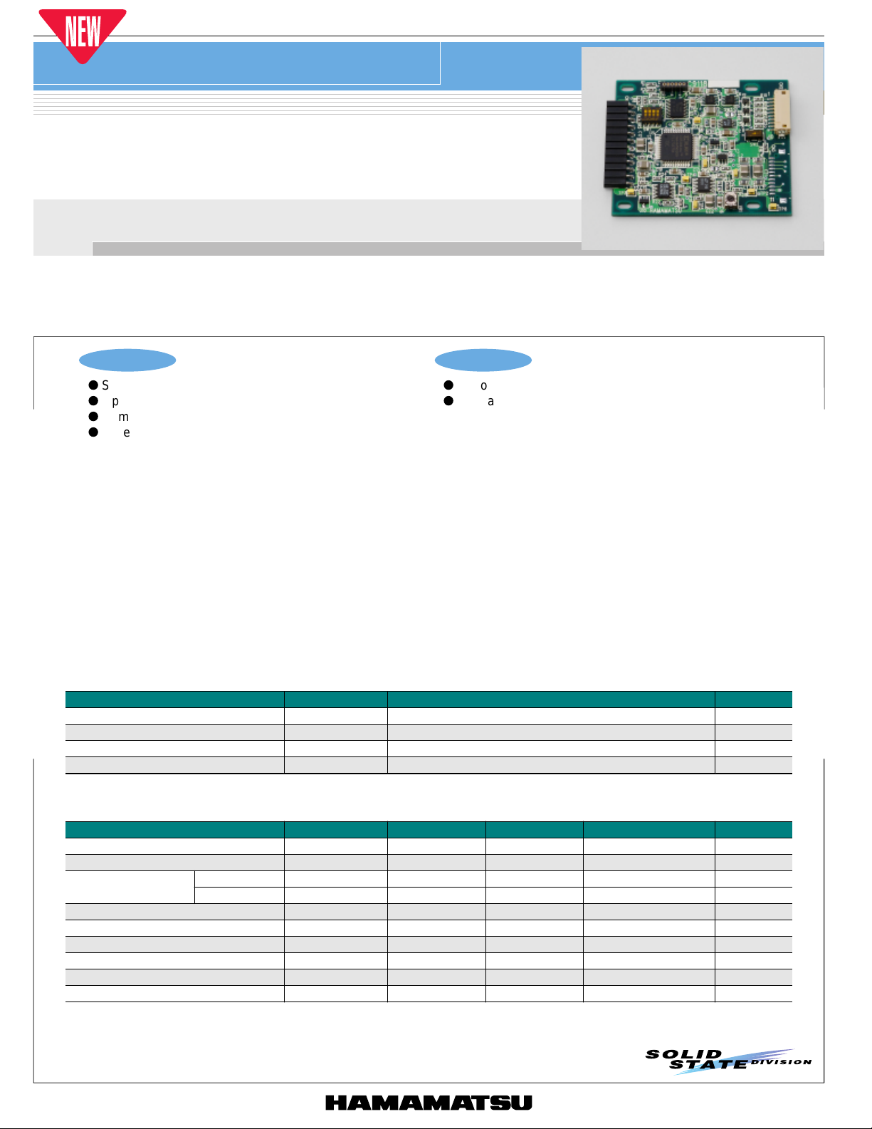
C9118 series
Compact, easy-to-use driver circuit
C9118 series CMOS driver circuit is designed for S8865 series photodiode array with amplifier.
C9118 series operates a linear image sensor by just inputting two signals (M-CLK and M-RESET) and a signal +5 V supply. C9118 series is
assembled on a compact board measuring 48 × 56 mm and allows downsizing of the measurement equipment.
C9118 is intended for single use or parallel connections, while C9118-01 is suitable for cascade connections.
C9118 series does not include S8865 series photodiode array with amplifier, so select the desired photodiode array and order it separately.
Features
l
Single power supply (+5 V) operation
l
Operation with two input signals (M-CLK and M-RESET)
l
Compact: 48 × 56 mm
l
Assembled with low profile components
Applications
l
Various types of image acquisition
l
Optical detection equipment
■ Absolute maximum ratings (Ta=25 °C)
Parameter Symbol Value Unit
Supply voltage Vcc +7 V
Digital input voltage - V V
Operating temperature Topr 0 to 50 *
Storage temperature Ts tg 0 to 70 *
*1: No condensation
1
1
°C
°C
■ Specifications (Ta=25 °C)
Parameter Symbol Min. Typ . Max. Unit
Rated voltage - 4.9 5.0 5.2 V
Current consumption +Is - 65 75 mA
Digital input
M-RESET pulse width (Low level) TpwstRESET1 10 - - µs
M-CLK frequency f
Digital rise/fall times t
Data rate fV 1 - 1000 kHz
Offset output Voffset - 0.5 - V
VIDEO saturation output *
*2: From offset value.
PRELIMINARY DATA
Jan. 2003
High level V
Low level V
2
IH
IL
CLK
TLH
THL
/ t
Vast - 4 . 0 - V
2.0 - V V
0- 0.8V
40 - 4000 kHz
- 20 30 ns
1
Page 2
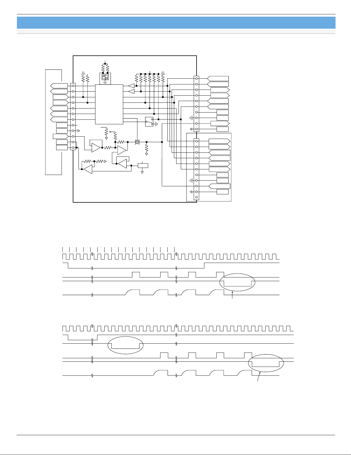
■ Block diagram
S8865 SERIES
CLK
RESET
Trig
EOS
EXTSP
Vms
Vg
Vdd
GND
Video
Vref
Vp
CN1
+Vp
Driver circuit for photodiode array with amplifier
+Vcc
+Vcc
SW2
+Vcc
REF
+Vcc
+Vcc
SW1
CONTROLLER
+Vp
+
-
+
1: TOP
2: END
1
2
VR1
+Vcc
+
-
+
C9118 series
CN2
M-CLK
M-RESET
TRIGGER
L-EOS
IN-START
GAIN
+5 V
GND
VIDEO
GND
CN3
M-CLK
M-RESET
TRIGGER
L-EOS
EXTSP2
GAIN
+5 V
GND
VIDEO
GND
■ Timing chart
Timing chart of first stage sensor when used singly or in cascade connection
2 3 14 15 16 17 18 19 20
1
M-CLK
M-RESET
TRIGGER
L-EOS
VIDEO
Timing chart of second and subsequent stage sensors when used in cascade connection
M-CLK
M-RESET
IN-START
TRIGGER
L-EOS
VIDEO signal is output right after EXTSP2 signal input from previous stage
C9118-01 ONLY
KACCC0187EA
Last stage sensor signal is output when
used in cascade connection.
VIDEO
Last stage sensor signal is output when
used in cascade connection
KACCC0188EA
2
Page 3

Driver circuit for photodiode array with amplifier
C9118 series
■ Connection examples
Single or parallel readout example (C9118) Cascade readout example (C9118-01)
Simultaneous integration/output
(effective for high-speed processing)
S8865
SERIES C9118
CN2
SCAN
DIRECTION
S8865
SCAN
DIRECTION
SCAN
DIRECTION
SERIES
S8865
SERIES C9118
C9118
CN2
CN2
■ Dimensional outline (unit: mm)
25
EXTERNAL
CONTROLLER
EXTERNAL
CONTROLLER
EXTERNAL
CONTROLLER
KACCC0189EA
56
32 38
Simultaneous integration/serial output
(Simplifies external processing circuit)
S8865
SERIES C9118-01
CN2
CN3
S8865
SCAN
DIRECTION
2
SERIES
S8865
SERIES C9118-01
C9118-01
CN2
CN3
CN2
CN3
4 × (2 ×) R1.2
EXTERNAL
CONTROLLER
ACCESSORY
CABLE
KACCC0190EA
SCAN
DIRECTION
51.2
2.5
CN1
1
42
12
6
8832
Component mounting height: 3.6 mm
2.5
■ Accessory
· Connectorized cable
This cable is for hooking up an external unit (power supply, pulse
generator, etc.) to the CN2 connector of C9118 driver circuit.
Pin No. and cable color coding are shown in the table at the right.
Connector: DF-13-10S-1.25C (Hirose Electric)
Terminal: DF13-2630SCFA (gold plating)
Cable: Conforms to UL1007 AWG28.
CN2
CN3
3.6
48
CN3 is installed only for C9118-01.
1.6
KACCA0124EA
Pin connection (CN2)
Pin No. Color Pin No. Color
➀ Brown ➅ Blue
➁ Red ➆ Purple
➂ Orange ➇ Gray
➃ Yellow ➈ White
➄ Green ➉ Black
100 mm
KACCC0198EA
3
Page 4

Driver circuit for photodiode array with amplifier
C9118 series
■ Pin assignment of I/O connector
<CN1>
For connection to S8865 photodiode array
Connector type: 801-93-012-20-001 PRECI-DIP (made by DURTAL) or equivalent
Pin No. Terminal Name I/O Description
1 RESET O
2 CLK O Sensor scan sync signal. Sensor starts scanning in synchronization with this signal.
3 Trig I For A/D conversion timing signals. Positive logic
4 EXTST O
5VmsO
6 Vdd O Sensor supply voltage
7 GND - Sensor GND
8 EOS I EOS (end of scan) signal of sensor. Negative logic
9 Video I Video output signal. Positive polarity
10 Vref O Reference voltage
11 Vgain O Sensor gain switching H: high gain, L: low gain
12 Vpd O Photodiode voltage
<CN2>
Used to connect the first stage to an external I/O during parallel readout or serial readout
For the second and subsequent stages during serial readout, CN2 is used to connect to CN3 at preceding stage.
Note 1) CN3 is installed only for C9118-01 (for serial readout).
Connector type: DF13-10P-1.25H (50) (made by Hirose Electric)
Pin No. Terminal Name I/O Description
1 M-RESET I
2 M-CLK I
3 TRIGGER O For A/D conversion timing signals. Positive logic
4 L-EOS O EOS (end of scan) signal of all sensors during parallel or serial readout. Negative logic
5 IN-START I
6 GAIN I External setting for sensor gain H: high gain, L: low gain
7GND-Circuit GND
8 +5 V I +5 V power supply
9 VIDEO O Video output signal. Positive polarity
10 A.GND O Video GND
Sensor scan start signal. Pulse width at High level nearly equals sensor integration
time.
High level at first stage during parallel or serial readout. At second and subsequent
stages during serial readout, this outputs the EOS pulse of preceding stage.
High level at first stage during parallel or serial readout. At second and subsequent
stages, this sets to Low level.
Sensor scan start signal. Pulse width at High level nearly equals sensor integration
time.
Sensor scan sync signal. Sensor and circuit start operating in synchronization with this
signal.
NC (no connection) at first stage during parallel or serial readout. At second and
subsequent stages during serial readout, this receives the EOS pulse of preceding
stage.
4
Page 5

Driver circuit for photodiode array with amplifier
C9118 series
<CN3>
Used to connect to CN2 at next stage during serial readout. (CN3 is installed only for C9118-01.)
Note 2) CN3 is installed only for serial readout.
Note 3) Pin No. 1 to 4 and 6 to 10 connect to the same pin No. of CN2 as common lines.
Connector type: DF13-11P-1.25H (50) (made by Hirose Electric)
Pin No. Terminal Name I/O Description
1 M-RESET I
Sensor scan start signal. Pulse width at High level nearly equals sensor integration
time.
2 M-CLK I Sensor scan sync signal. Sensor starts scanning in synchronization with this signal.
3 TRIGGER O For A/D conversion timing signals. Positive logic
4 L-EOS O EOS (end of scan) signal of all sensors during parallel or serial readout. Negative logic
5 EXTSP2 O Video signal scan start signal at second stage during serial readout. Negative logic
6 GAIN I External setting for sensor gain H: high gain, L: low gain
7GND-Circuit GND
8 +5 V I +5 V power supply
9 VIDEO O Video output signal. Positive polarity
10 A.GND O Video GND
11 NC - No connection
■ P arallel readout and serial readout settings
<Parallel readout setting>
ON
1432
<First stage setting for serial readout>
ON
1432
<Second stage to second from last stage setting for serial readout>
ON
1432
<Last stage setting for serial readout>
ON
1432
Set SW1 and SW2 to OFF as shown at left.
(SW3 and SW4 have no connection)
Set SW1 to OFF and SW2 to ON as shown at left.
(SW3 and SW4 have no connection)
Set SW1 and SW2 to ON as shown at left.
(SW3 and SW4 have no connection)
Set SW1 to ON and SW2 to OFF as shown at left.
(SW3 and SW4 have no connection)
KACCC0191EA
Information furnished by HAMAMATSU is believed to be reliable. Howe ver, no responsibility is assumed for possible inaccuracies or omissions.
HAMAMATSU PHOTONICS K.K., Solid State Division
1126-1 Ichino-cho, Hamamatsu City, 435-8558 Japan, Telephone: (81) 053-434-3311, Fax: (81) 053-434-5184, http://www.hamamatsu.com
U.S.A.: Hamamatsu Corporation: 360 Foothill Road, P.O.Box 6910, Bridgewater, N.J. 08807-0910, U.S.A., Telephone: (1) 908-231-0960, Fax: (1) 908-231-1218
Germany: Hamamatsu Photonics Deutschland GmbH: Arzbergerstr. 10, D-82211 Herrsching am Ammersee, Germany, Telephone: (49) 08152-3750, Fax: (49) 08152-2658
France: Hamamatsu Photonics France S.A.R.L.: 8, Rue du Saule Trapu, Parc du Moulin de Massy, 91882 Massy Cedex, France, Telephone: 33-(1) 69 53 71 00, Fax: 33-(1) 69 53 71 10
United Kingdom: Hamamatsu Photonics UK Limited: 2 Howard Court, 10 Tewin Road, Welwyn Garden City, Hertfordshire AL7 1BW, United Kingdom, Telephone: (44) 1707-294888, Fax: (44) 1707-325777
North Europe: Hamamatsu Photonics Norden AB: Smidesvägen 12, SE-171 41 Solna, Sweden, Telephone: (46) 8-509-031-00, Fax: (46) 8-509-031-01
Italy: Hamamatsu Photonics Italia S.R.L.: Strada della Moia, 1/E, 20020 Arese, (Milano), Italy, Telephone: (39) 02-935-81-733, Fax: (39) 02-935-81-741
Specifications are subject to change without notice. No patent rights are granted to any of the circuits described herein. ©2003 Hamamatsu Photonics K.K.
Cat. No. KACC1087E02
Jul. 2003 DN
5
 Loading...