

Page 1
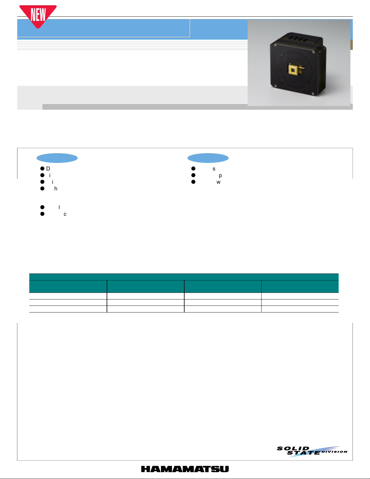
IMAGE SENSOR
CCD multichannel detector head
C7973
Designed for back-thinned CCD area image sensor
C7973 is a high sensitivity multichannel detector head for use with back-thinned FFT-CCD area image sensors (S7963, S7964, S7965) that offer
high UV sensitivity and quantum efficiency. C7973 incorporates a low-noise driver/amplifier circuit that provides reliable operation from simple
external signals. C7973 includes a highly stable temperature controller that cools the sensor to a preset temperature level (Ts= -10 ˚C) as soon as
the power is turned on. If the cooler fails and causes internal circuitry to overheat, the built-in protection circuit automatically turns off the power to
the thermoelectric cooler. Despite its compact size, the housing configuration is designed for good heat dissipation, and threaded mounting holes
on the front panel allow connections to other devices such as monochrometers.
Features
l
Designed for back-thinned CCD area image sensor *
l
Line binning operation/area scanning operation *
l
Driver/amplifier circuit for low noise CCD operation
l
Highly stable temperature controller
Cooling temperature: -10 ± 0.05 ˚C
(Ta=10 to 35 ˚C)
l
Simple signal input operation
l
Compact configuration
The table below shows CCD area image sensors applicable for C7973.
Since C7973 does not include aCCD area image sensor, so select the desired sensor and order itseparately.
CCD area image sensor
Type No. Number of pixels Number of active pixels
S7963 80 × 72 64 × 64 1.536 × 1.536
S7964 124 × 56 108 × 48 2.592 × 1.152
S7965 232 × 56 216 × 48 5.184 × 1.152
*1: In normal CCD image sensors that receive light from the front surface, the active area is covered with electrodes for charge transfer.
These electrodes cut off UV radiation incident on the image sensor and also reduce the quantum efficiency. In contrast, backthinned CCD image sensors have a unique structure in which the back of the active area is finely ground to allow light to enter from
the back surface. This structure ensures high UV sensitivity and quantum efficiency because incident light need not pass through the
electrodes.
*2: The FFT-CCD was originally designed as a two-dimensional image sensor. However, it can be operated like a linear image sensor
having a large active area by transferring all the pixel signals in the vertical direction to the horizontal register (this is referred to as
line binning).
1
2
Applications
l
Fluorescence spectroscopy
l
Raman spectroscopy
l
Other low-light-level detection
Active area
[mm (H) × mm (V)]
1
Page 2
CCD multichannel detector head
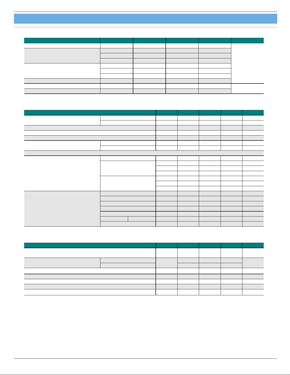
■ Absolute maximum ratings
Parameter Symbol Min. Typ. Max. Unit
Supply voltage (for digital circuitry) V
D1
V
A1+
V
A1-
V
A2
V
D2
-0.5 - +7
- - +18
- - -18Supply voltage (for analog circuitry)
- - +30
--+7
Vp- -+7Supply voltage
V
F
Digital input voltage - - - V
--+14
D (1, 2)
Operating temperature Topr +10 - +35
Storage temperature Tstg 0 - +70
■ Electrical characteristics
(Ta=25 °C, V
,
=+5 V, V
Digital input
CLK frequency f
Data video readout frequency fv - - f
Start pulse width tst 1/f
Digital output
Power supply operating conditions
Voltage
Current
)
+
=+15 V, V
)
-
= -15 V, V) =+24 V, V, =+5 V, Vp=+5 V, V.=+12 V, unless otherwise noted)
Parameter Symbol Min. Typ. Max. Unit
High level V
Low level V
High level (Io= -6 mA) V
Low level (Io=+6 mA) V
Digital circuitry V
V
V
Other
IH
IL
CLK
IH
IL
D
A1+
A1-
VA2
V
D2
Vp +4.75 +5.0 +5.25 V
V
F
+2.0 - +5.0 V
-0.5 - +0.8 V
- - 1 MHz
CLK
- - s
+2.0 - - V
--+0.8V
+4.75 +5.0 +5.25 V
+14.5 +15.0 +15.5 V
-14.5 -15.0 -15.5 VAnalog circuitry
+23.5 +24.0 +24.5 V
+4.75 +5.0 +5.25 V
+11.75 +12.0 +12.75 V
VD1 (+5 VDC) - - - +200 mA
V
(+15 VDC) - - - +100 mA
A1+
V
(-15 VDC) - - - -100 mA
A1-
VA2 (+24 VDC) - - - +30 mA
VD2 (+5 VDC) - - - +30 mA
Vp (+5 VDC) Ta=25 °C - - +1.0 +2.0 A
VF (+12 VDC) - - +100 - mA
/4 Hz
CLK
C7973
V
°C
■ Electrical and optical characteristics
(Ta=25 °C, Ts= -10 °C, V
,
=+5 V, V
Parameter Symbol Min. Typ. Max. Unit
Spectral response range
Full well capacity
Conversion gain *
3
Dark current DS - 60 180 e-/pixel/s
Readout noise Nr - 30 60 e-rms
Dynamic range DR - 100,000 - Photo response non-uniformity *
*3: Including the circuit gain.
*4: Measured at 50 % of the full well capacity.
)
+
=+15 V, V
Vertical - 300,000 Horizontal
4
)
-
= -15 V, V) =+24 V, V, =+5 V, Vp=+5 V, V.=+12 V)
l
Fw
-
- 600,000 -
200 to
1100
Sv - 4 - µV/e
PRNU - ±3 ±10 %
-nm
-
e
-
2
Page 3
CCD multichannel detector head
C7973
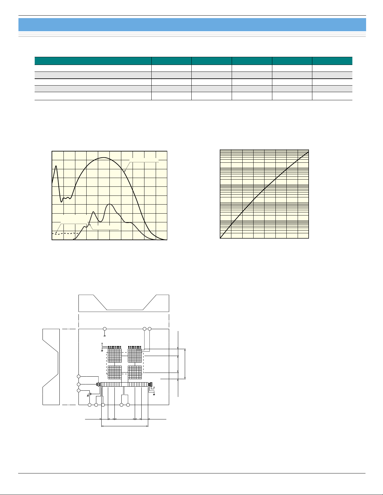
■ Specifications for temperature controller (C7041)
(Ta=25 °C, Ts= -10 °C, V
Parameter *
,
=+5 V, V
5
Cooling temperature Ts -11 -10 -9 °C
Temperature control range
Power dissipation of TE-cooler element Pp - - 2 W
Cool down time to reset temperature to - - 5 min.
Setting temperature for overheat protection *
*5: Other functions include error display, automatic power off, and detection of electrical opens and shorts by the thermosensor.
*6: Temperature at back side of housing (between housing and fan).
)
+
=+15 V, V
)
-
= -15 V, V) =+24 V, V, =+5 V, Vp=+5 V, V.=+12 V)
Symbol Min. Typ. Max. Unit
DTs
6
To - +45 - °C
-0.05 - +0.05 °C
■ Spectral response (without window)
100
90
80
70
60
50
40
30
FRONT-SIDED
(UV COAT)
20
QUANTUM EFFICIENCY (%)
10
0
200 400 600 800 1000 1200
FRONT-SIDED
BACK-THINNED
WAVELENGTH (nm)
■ Device structure
THINNING
(Typ. Ta=25 ˚C)
KMPDB0058EA
■ Dark current vs. temperature
10000
1000
/pixel/s)
-
100
10
1
DARK CURRENT (e
0.1
-50 -40 -30
-20
0-10 10 20 30
TEMPERATURE (˚C)
(Typ.)
KMPDB0037EA
THINNING
RG
RD
OD
P2V
56
P2H
P1V
10
11
4 BEVEL
M
4 BLANK4 BLANK
BEVELBEVEL
ACTIVE PIXEL
TOTAL PIXEL
4 BEVEL
KMPDC0134EA
SS
13
N
4
3
2
1
2
3
4
SGOGOS
4
P1H
ACTIVE PIXEL
TOTAL PIXEL
1
12
3
2
14
3
Page 4

■ Block diagram
CCD AREA IMAGE SENSOR
S7963, S7964, S7965
P+
TE-COOLER
IG1H, IG2H
IG1V, IG2V
P1V, P2V, TG
SS, ISV, ISH
P-
TH1
TH2
OD
RD
OG
P1H, P2H
SG
RG
OS
REGULATOR
VDD
DRIVER
CCD multichannel detector head
TEMPERATURE CONTROLLER
VEE
PRE-AMP
INVERTER
TH.H
TIMING
GENERATOR
CLAMP
LED
BUFFER
LOW-PASS
FILTER
C7973
Vp (+5V)
P. GND
V
D2 (+5V)
D. GND
VF (+12V)
F. GND
Temp Monitor
Cooling Control
V
D1 (+5V)
D. GND
VA1+ (+15V)
VA1- (-15V)
A. GND
A2 (+24V)
V
Start
CLK
EOS
Trigger
Mode Select
Data Video
■ Timing chart of line binning operation
Start
CLK
P1V
P2V
TG
P1H
P2H
SG
RG
Clamp
EOS
Trigger
Data Video
V-ch1 V-ch2 V-ch(M) H-ch1 H-ch2
KACCC0163EA
H-ch11H-ch10
M=56, 72 N=80, 124, 232
V-ch1--V-ch4, V-ch (M-3)--V-ch (M): ISOLATION PIXELS
H-ch1--H-ch4, H-ch (N-3)--H-ch (N): BLANK PIXELS
H-ch5--H-ch8, H-ch (N-7)--H-ch (N-4): ISOLATION PIXELS
H-ch(N-9)H-ch(N-10)
H-ch(N)
KACCC0164EA
4
Page 5
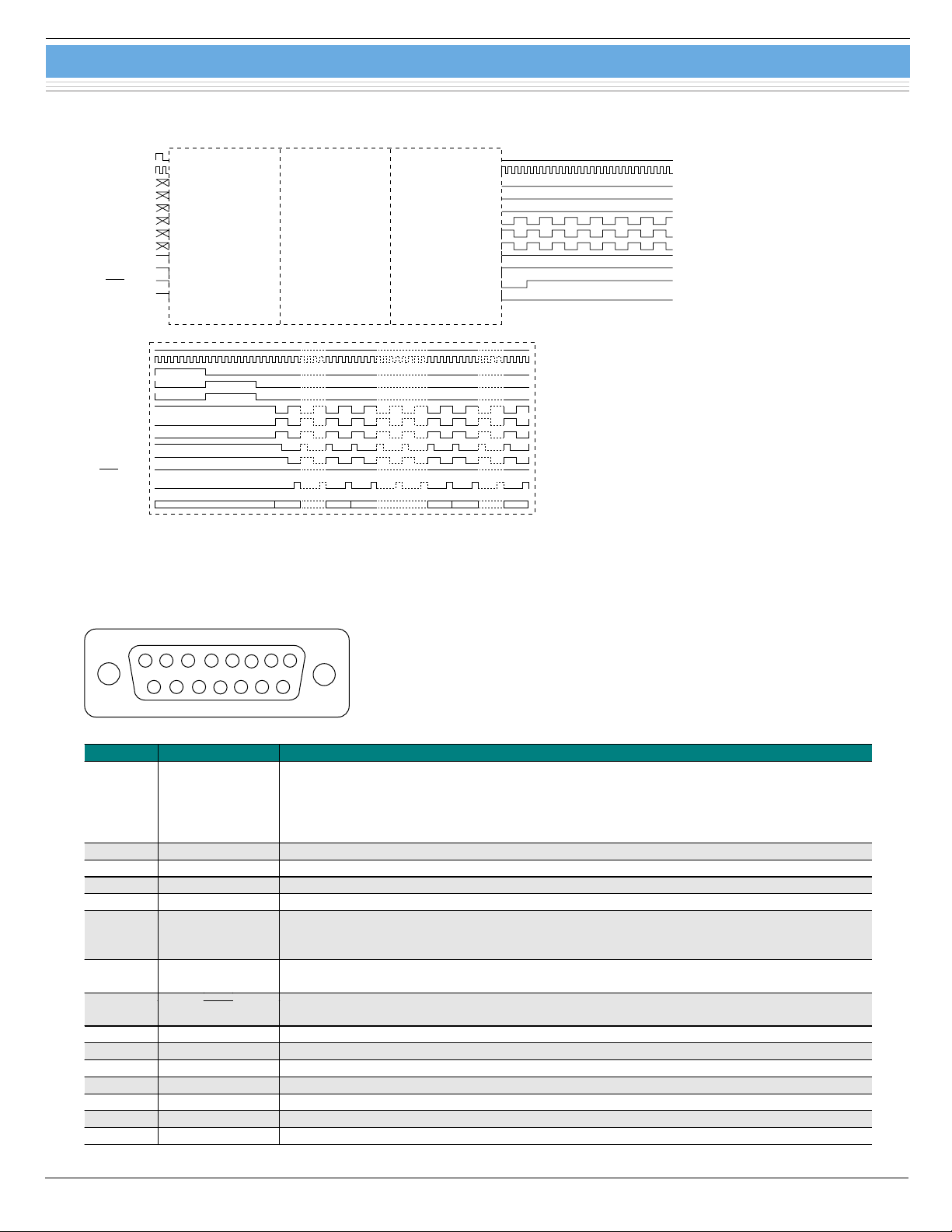
■ Timing chart of area scanning operation
Start
CLK
P1V
P2V
TG
P1H
P2H
SG
RG
Clamp
EOS
Trigger
Data Video
Start
CLK
P1V
P2V
TG
P1H
P2H
SG
RG
Clamp
EOS
Trigger
Data Video
BLOCK 1 ••••••••• BLOCK M
V-ch1 H-ch1 H-ch10 H-ch11
NOTE) M=56, 72 N=80, 124, 232
CCD multichannel detector head
H-ch (N-10)H-ch (N-9)H-ch (N
C7973
)
KACCC0165EA
■ Pin connection of "SIGNAL I/O" connector
15-pin D-sub connector
2345678
1
131415
Pin No. Terminal name Description
1 Mode select
2 Data video Analog video output. Positive polarity
3V
4 V
5V
(+15 V) Analog power supply
A1+
(-15 V) Analog power supply
A1-
(+5 V) Digital power supply
D1
6 Start
7CLK
8
EOS
9 A. GND Analog ground
10 A. GND Analog ground
11 VA2 (+24 V) Analog power supply
12 D. GND Digital ground
13 D. GND Digital ground
14 D. GND Digital ground
15 Trigger Digital output signal for A/D conversion. HCMOS compatible. Positive logic.
9101112
KACCC0069EA
Digital input signal used to select between the line binning operation and area scanning
operation.
HCMOS compatible.
High level or left open: line binning operation
Low level: area scanning operation
Digital input signal for initializing the circuit.
HCMOS compatible. Positive logic.
The interval of the Start pulses determines the integration time of the CCD image sensor.
Digital input signal for operating the circuit.
HCMOS compatible. Rising edge operation.
Digital input signal for indicating end-of-scan of the image sensor.
HCMOS compatible. Negative logic.
5
Page 6
CCD multichannel detector head
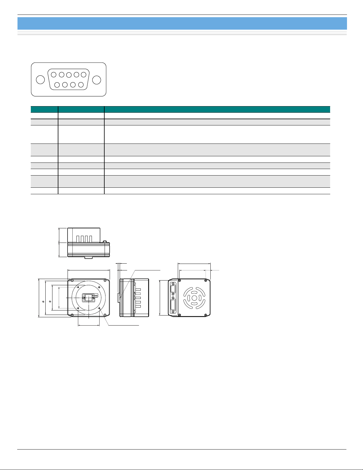
■ Pin connection of "TE CONTROL I/O" connector (C7041)
9-pin D-sub connector
2345
1
9
8
67
KACCC0075EA
Pin No. Terminal name Description
1V
2 Temp monitor Analog output signal of the temperature of the CCD image sensor
3 Cooling control
4 Vp (+5 V)
5V
6 D. GND Ground
7 D. GND Ground
8 P. GND
9 F. GND Power supply return for cooling fan
Available for using same power supply (+5 V) for "+VD2" and "+Vp".
(+5 V) Digital power supply
D2
Digital input signal for starting to cool down. HCMOS compatible.
High level or left open: cooling
Low level: stand-by
Power supply for the thermoelectric cooler in the CCD image sensor.
(Please use AWG 18 wire)
(+12 V) Power supply for cooling fan
F
Power supply return of the thermoelectric cooler mounted in the CCD image sensor.
(Please use AWG 18 wire)
C7973
■ Dimensional outline (unit: mm)
35.0
34.0
100.0
60.0
80.0
90.0
50.0
50.0
(4 ×) M3 DEPTH 4
4.0
0.5
FOCAL PLANE
82.0
TE-control I/O Signal I/O
62.0
77.0
11.0
KACCA0110EA
6
Page 7
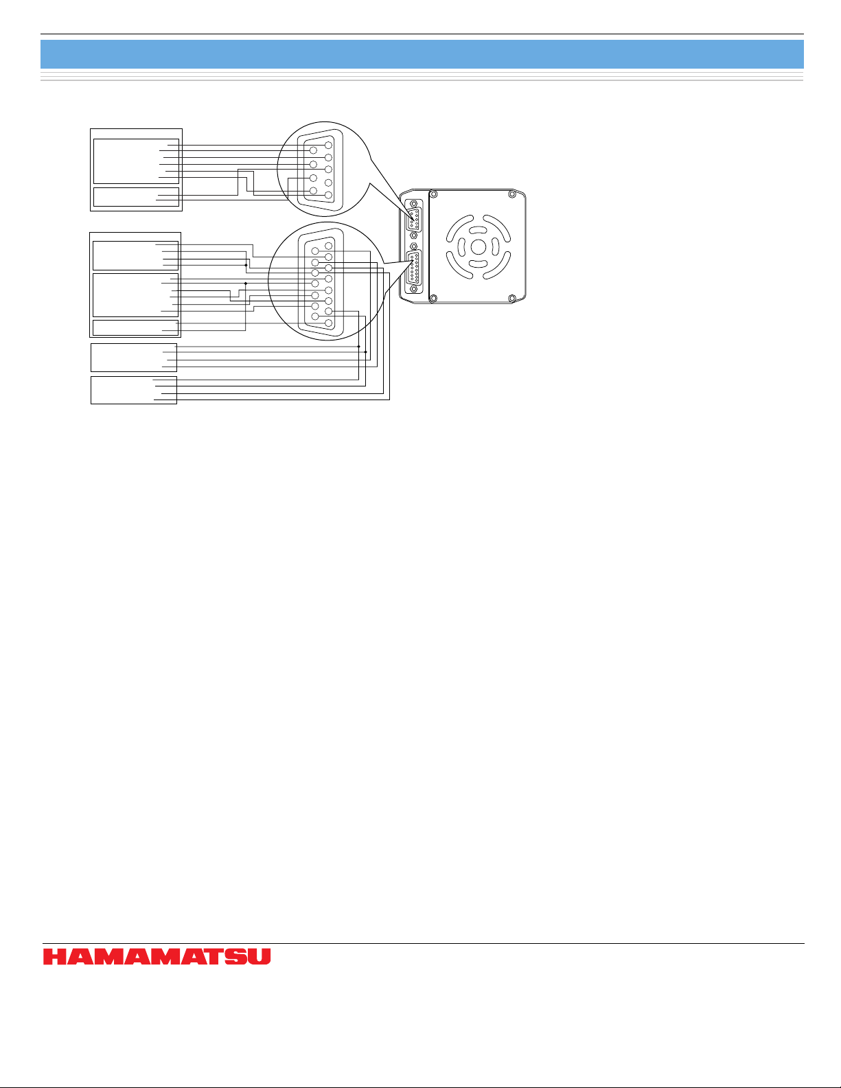
■ Connection example
TE CONTROLLER
POWER SUPPLY
VF (+12 V)
F. GND
P
(+5 V)
V
P. GND
D2
(+5 V)
V
D. GND
CONTROLLER
Cooling
D. GND
I/O SIGNAL
PULSE GENERATOR
POWER SUPPLY
CONTROLLER
S/H or A/D
OSCILLOSCOPE
CLK
D. GND
Start
D. GND
V
D1
(+5 V)
D. GND
A1+
(+15 V)
V
A1-
(-15 V)
V
A2
(+24 V)
V
A. GND
Mode Select
D. GND
Analog Input
A. GND
S/H Input
D. GND
CH1
GND
Ext.Trig
GND
CCD multichannel detector head
5
9
4
8
3
7
2
6
1
8
15
7
14
6
13
5
12
4
11
3
10
2
9
1
KACCC0166EA
C7973
Information furnished by HAMAMATSU is believed to be reliable. However, no responsibility is assumed for possible inaccuracies or omissions.
Specifications are subject to change without notice. No patent rights are granted to any of the circuits described herein. ©2003 Hamamatsu Photonics K.K.
HAMAMATSU PHOTONICS K.K., Solid State Division
1126-1 Ichino-cho, Hamamatsu City, 435-8558 Japan, Telephone: (81) 053-434-3311, Fax: (81) 053-434-5184, http://www.hamamatsu.com
U.S.A.: Hamamatsu Corporation: 360 Foothill Road, P.O.Box 6910, Bridgewater, N.J. 08807-0910, U.S.A., Telephone: (1) 908-231-0960, Fax: (1) 908-231-1218
Germany: Hamamatsu Photonics Deutschland GmbH: Arzbergerstr. 10, D-82211 Herrsching am Ammersee, Germany, Telephone: (49) 08152-3750, Fax: (49) 08152-2658
France: Hamamatsu Photonics France S.A.R.L.: 8, Rue du Saule Trapu, Parc du Moulin de Massy, 91882 Massy Cedex, France, Telephone: 33-(1) 69 53 71 00, Fax: 33-(1) 69 53 71 10
United Kingdom: Hamamatsu Photonics UK Limited: 2 Howard Court, 10 Tewin Road, Welwyn Garden City, Hertfordshire AL7 1BW, United Kingdom, Telephone: (44) 1707-294888, Fax: (44) 1707-325777
North Europe: Hamamatsu Photonics Norden AB: Smidesvägen 12, SE-171 41 Solna, Sweden, Telephone: (46) 8-509-031-00, Fax: (46) 8-509-031-01
Italy: Hamamatsu Photonics Italia S.R.L.: Strada della Moia, 1/E, 20020 Arese, (Milano), Italy, Telephone: (39) 02-935-81-733, Fax: (39) 02-935-81-741
Cat. No. KACC1070E02
Feb. 2003 DN
7
 Loading...