

Page 1
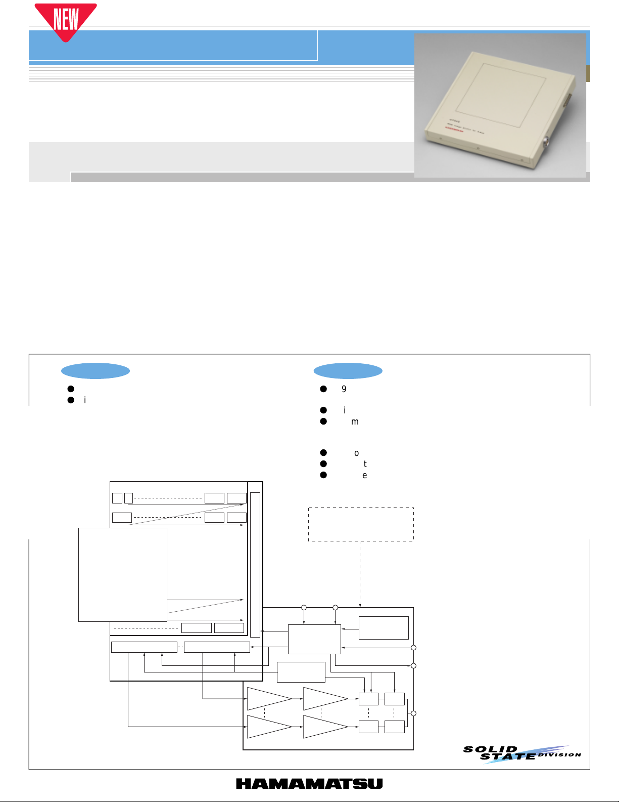
IMAGE SENSOR
Flat panel sensor
C7942CA, C7943CA
Acquire digital X-ray image in real time and 170 & 176 mm diagonal size
Hamamatsu C7942CA and C7943CA Flat Panel Sensors are digital X-ray image sensors newly developed as key devices for non-destructive
inspection, biomedical imaging, X-ray microscopy and other real-time X-ray imaging applications requiring high resolution and high image quality.
C7942CA and C7943CA consist of a sensor board and a control board, both assembled in a thin, flat and compact package. The sensor board
contains a CsI scintillator plate, a two-dimensional photodiode array with FET switches and a signal processing IC chip. The photodiode array has
a 2400 × 2400 (C7942CA) or 1248 × 1248 (C7943CA) pixel format with minimized blooming and is highly sensitive to bluish green light emitted
from the CsI scintillator. Each row of pixels is addressed in sequence by the vertical shift register connected to the gate line.
Light emission occurs when X-rays are absorbed in the CsI scintillator. This light emission enters directly into the two-dimensional photodiode
array where an electric charge is stored in each pixel according to the light intensity. This charge is then transferred to the corresponding data line
by applying a control signal to the vertical shift register.
The sensor board also has 8 charge sensitive amplifier arrays each having 300 channel (C7942CA) or 156 channel (C7943CA) amplifiers with a
horizontal shift register. These amplifiers with a total of 2400 channels (C7942CA) or 1248 channels (C7943CA) are connected to a CDS
(Correlated Double Sampling) circuit that senses the charge on each video line and sends it as the analog video signal from each amplifier array.
The control board converts the analog video signal into a 12-bit digital signal and outputs it to an external frame grabber from a 12-bit parallel port.
C7943CA delivers a frame rate of 30 frames per second using 4 × 4 binning and is ideal for high frame rate applications. On the other hand,
C7942CA is ideal for applications requiring high resolution because of its 50 µm pixel size. Massive digital image data can easily be monitored on
a display unit by using a frame grabber board and video memory installed in the PC. C7942CA and C7943CA will prove ideal tools for real-time Xray imaging and processing where easy-to-use, high-resolution X-ray digital image sensors are needed.
Applications
l
Non-destructive inspection
l
Digital X-ray photography
■ Block diagram (C7942CA)
PIXEL NUMBER
12
SCINTILLATOR
(120 mm × 120 mm)
AMP ARRAY No. 1
24002339
480047992401
PHOTODIODE
ARRAY
57600005759999
AMP ARRAY No. 8
SHIFT REGISTER
IntExt
TIMING
PULSE
GENERATOR
BIAS
GENERATER
Features
l
C7942CA: 2400 × 2400 pixels
C7943CA: 1248 × 1248 pixels
l
Digital output (12 bit)
l
Dynamic picture image
C7942CA: 9 frame/s (4 × 4 binning)
C7943CA: 30 frame/s (4 × 4 binning)
l
Low noise and wide dynamic range
l
Compact package
l
Easy use
EXTERNAL POWER SUPPLY
A. Vdd, D. Vdd V (±7.5)
(not attached)
IntExt
BINNING
(bin0, bin1)
OSCILLATOR
ExtTrg
Vsync
Hsync
Pclk
BUFFER
AMP
BUFFER
AMP
PROCESSING
AMP
PROCESSING
AMP
A/D
FIFO
A/D FIFO
VIDEO OUTPUT
(12 BIT DIGITAL)
KACCC0137EA
1
Page 2
■
Vsync+
(RS-422)
Hsync+
(RS-422)
Hsync+
(RS-422)
Pclk+
(RS-422)
Data1 - 12
(RS-422)
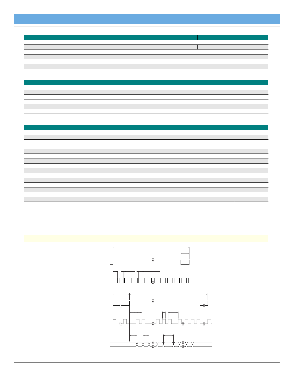
In case of C7942CA, the number of n is 300.
In case of C7943CA the number of n is 156.
Tvc (1 FRAME)
Thd
Thdpw Thc (1 LINE)
Tvdpw
Thdpw Thc (1 LINE)
Tpd
Tpdb
Tpc (1 PIXEL)
Tppw
Tpdb
1 2 n-1 n n+1
8n-1
8n
TdcTdd
Functional specification
Flat panel sensor
C7942CA, C7943CA
Parameter C7942CA C7943CA
Readout Charge amplifier array
Feedback capacitance of each amplifier 0.15 pF 0.6 pF
Video output (Data1 - 12) RS-422 (differential) 12 bit
Output data rate 15.15 MHz
Synchronous signal (Vsync, Hsync, Pclk) RS-422 (differential)
bin0, 1, ExtTrg, IntExt TTL
■
Absolute maximum ratings (Ta=25 °C)
Parameter Symbol Valu e Unit
Supply voltage for digital circuitry (+5 V) D.vdd +6.0 V
Supply voltage for analog circuitry (+5 V) A.vdd +6.0 V
Supply voltage for analog circuitry (±7.5 V) V(+/-7.5) ±12 V
Input voltage (bin0, 1, ExtTrg, IntExt) Vin 0 to 6.0 V
Operating temperature (not condensed) Topr 0 to +35 °C
Storage temperature (not condensed) Tstg 0 to +50 °C
■
Specification (Unless otherwise noted, Typ. Ta=25 °C A.vdd= 5.0 V, D.vdd= 5.0 V, V (±7.5)= ±7.5 V)
Parameter Symbol C7942CA C7943CA Unit
Pixel size 50 100 µm
Active area 120 × 120 124.8 × 124.8 mm
Pixel number
5.76
(2400 × 2400)
1.56
(1248 × 1248)
M pixels
Number of active pixels (horizontal × vertical) - 2240 × 2368 1216 × 1232 pixels
Frame speed (single operation) Sf (int) 2 7 frame/s
Frame speed (2 × 2 binning) 4 15 frame/s
Frame speed (4 × 4 binning) 9 30 frame/s
Frame speed external (single operation) Sf (ext) Sf (int) to 0.1 Sf (int) to 0.1 frame/s
Noise (rms.) N (rms.) 1100 2300 electrons
Saturation charge Csat 2.2 10 M electrons
Resolution Reso 8 5 line pairs/mm
Dynamic range 2000 4300 Defect line * - 20 Max. 10 Max. lines
Scintillator - CsI -
* Without a couple of adjacent defect line that has no response.
■ Timing chart
To acquire images through an image grabber board, parameters that match the following timing chart should be described in the
software program or parameter file.
Internal mode
KACCC0138EB
2
Page 3
ExtTrg
(TTL)
Vsync+
(RS-422)
Flat panel sensor
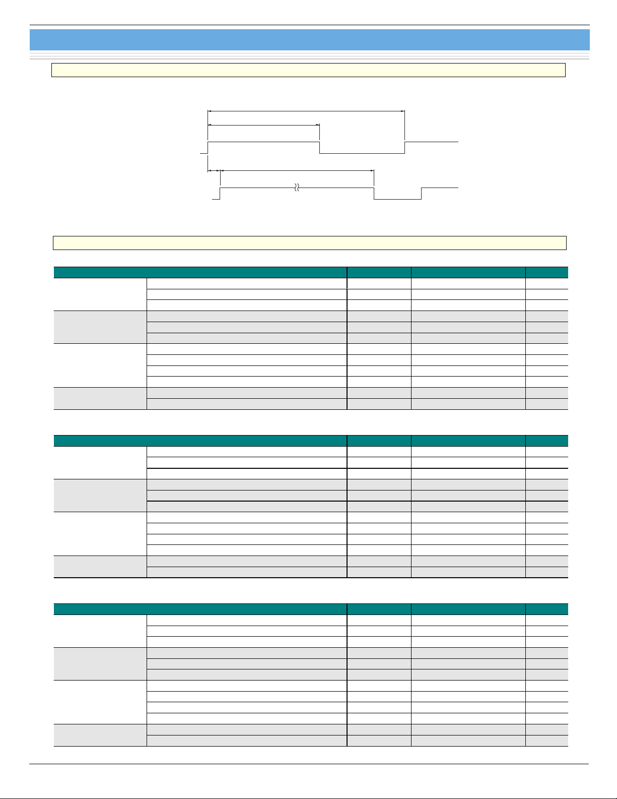
External mode
FROM Tvc TO 10 s
RECOMMENDATION: 50 % OF FRAME TIME
Tvc - TvdpwTvd
C7942CA, C7943CA
1 × 1 mode (Typ.)
Pclk
Data1-12
2 × 2 mode (Typ.)
Hsync
Pclk
Data1-12
Hsync+, Pclk and Data 1-12 are the same as internal trigger mode.
KACCC0139EB
C7942CA
Parameter Symbol Value Unit
Delay time (only external trigger mode) Tvd 390 µs
Cycle time Tvc 470 msVsync
Dummy pulse width Tvdpw 770 µs
Delay time Thd 1.4 µs
Cycle time Thc 190 µsHsync
Dummy pulse width Thdpw 35 µs
Delay time Tpd 65 ns
Cycle time Tpc 66 ns
Pulse width Tppw 33 ns
Delay time between each block Tpdb 200 ns
Delay time Tdd 34 ns
Cycle time Tdc 66 ns
Parameter Symbol Value Unit
Delay time (only external trigger mode) Tvd 390 µs
Cycle time Tvc 230 msVsync
Dummy pulse width Tvdpw 770 µs
Delay time Thd 1.4 µs
Cycle time Thc 190 µs
Dummy pulse width Thdpw 110 µs
Delay time Tpd 65 ns
Cycle time Tpc 66 ns
Pulse width Tppw 33 ns
Delay time between each block Tpdb 200 ns
Delay time Tdd 34 ns
Cycle time Tdc 66 ns
4 × 4 mode (Typ.)
Parameter Symbol Value Unit
Delay time (only external trigger mode) Tvd 390 µs
Vsync
Pclk
Data1-12
Note) The numbers of siginificant figures is two. (except Tvc)
Cycle time Tvc 117 ms
Dummy pulse width Tvdpw 770 µs
Delay time Thd 1.4 µs
Cycle time Thc 190 µsHsync
Dummy pulse width Thdpw 150 µs
Delay time Tpd 65 ns
Cycle time Tpc 66 ns
Pulse width Tppw 33 ns
Delay time between each block Tpdb 200 ns
Delay time Tdd 34 ns
Cycle time Tdc 66 ns
3
Page 4

1 × 1 mode (Typ.)
Pclk
Data1-12
2 × 2 mode (Typ.)
Vsync
Hsync
Pclk
Data1-12
Flat panel sensor
C7942CA, C7943CA
C7943CA
Parameter Symbol Val ue Unit
Delay time (only external trigger mode) Tvd 210 µs
Cycle time Tvc 130 msVsync
Dummy pulse width Tvdpw 420 µs
Delay time Thd 1.8 µs
Cycle time Thc 110 µsHsync
Dummy pulse width Thdpw 22 µs
Delay time Tpd 65 ns
Cycle time Tpc 66 ns
Pulse width Tppw 33 ns
Delay time between each block Tpdb 200 ns
Delay time Tdd 33 ns
Cycle time Tdc 66 ns
Parameter Symbol Val ue Unit
Delay time (only external trigger mode) Tvd 210 µs
Cycle time Tvc 66 ms
Dummy pulse width Tvdpw 420 µs
Delay time Thd 1.8 µs
Cycle time Thc 110 µs
Dummy pulse width Thdpw 63 µs
Delay time Tpd 65 ns
Cycle time Tpc 66 ns
Pulse width Tppw 33 ns
Delay time between each block Tpdb 200 ns
Delay time Tdd 33 ns
Cycle time Tdc 66 ns
4 × 4 mode (Typ.)
Parameter Symbol Val ue Unit
Delay time (only external trigger mode) Tvd 210 µs
Cycle time Tvc 33 msVsync
Dummy pulse width Tvdpw 420 µs
Delay time Thd 1.8 µs
Cycle time Thc 110 µsHsync
Dummy pulse width Thdpw 84 µs
Delay time Tpd 65 ns
Pclk
Data1-12
Note) The numbers of siginificant figures is two.
Cycle time Tpc 66 ns
Pulse width Tppw 33 ns
Delay time between each block Tpdb 200 ns
Delay time Tdd 33 ns
Cycle time Tdc 66 ns
4
Page 5
Flat panel sensor
C7942CA, C7943CA
■ System requirements
To operate C7942CA and C7943CA Flat Panel Sensors at full performance, the following system and peripherals are required.
PC: IBM compatible PC running on Windows 98 or later operating system
Digital frame grabber card: Monochrome 16 bits or more, pixel clock 16 MHz or more, RS-422 interface synchronous signal (See
the frame grabber manual.)
The National Instruments IMAQ PCI-1424 (NI parts No. 777662-01) frame grabber with optional memory 64 MB (NI parts No.
920130-64) has been verified to successfully acquire 12-bit digital images from both C7942CA and C7943CA. The IMAQ PCI1422 (NI parts No. 777959-01) also acquires satisfactory images from C7943CA. You can utilize the demonstration software that
comes with the frame grabber as a simple view er, to acquire and save an image. To do so, refer to the frame grabber user’s guide
for how to use the camera information file for the demonstration software.
Po wer source: A. Vdd = +5.0 ± 0.1 V (700 mA), D. Vdd = +5.0 ± 0.1 V (1000 mA), V (±7.5) = ±7.5 ± 0.5 V (±100 mA). Use of a series
power supply is recommended. (Av oid using a switching power supply.) A power cable (terminated with an FGG.2B.307.CLAD92Z
plug at one end and open at the other end; 2 m; see Table 2.) comes supplied with C7942CA and C7943CA. An optional 36-pin
cable for interface with the 36-pin receptacle (see Table 1) on C7942CA and C7943CA is also available for synchronous signal
input, video output and external control.
The voltages described above are specified at the flat panel sensor side. The impedance of the power cable attached with the
flat panel sensor is low enough but it causes 0.1 V approx. drop. Therefore the voltage at the power source side should be set
0.1 V higher than the voltage specified above.
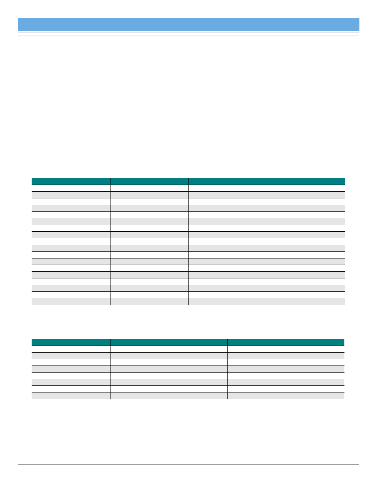
Table 1 Pin assignment of 36-pin receptacle
Pin No. Signal Pin No. Signal
1 Data1+ (MSB) 19 Data1- (MSB)
2 Data2+ 20 Data23 Data3+ 21 Data34 Data4+ 22 Data45 Data5+ 23 Data56 Data6+ 24 Data67 Data7+ 25 Data78 Data8+ 26 Data8-
9 Data9+ 27 Data910 Data10+ 28 Data1011 Data11+ 29 Data1112 Data12+(LSB) 30 Data12- (LSB)
13 bin0 (TTL) 31 Gnd
14 bin1 (TTL) 32 Gnd
15 ExtTrg (TTL) 33 IntExt (TTL)
16 Vsync+ 34 Vsync17 Hsync+ 35 Hsync18 Pclk+ 36 Pclk-
Unless otherwise noted, signal level is RS-422.
36-pin receptacle: TX20A-36R-D2GF1-A1L made by JAE (Japan Aviation Electronics Industry limited)
36-pin mating plug: TX20A-36PH1-D2P1-D1 made by JAE (Japan Aviation Electronics Industry limited)
Table 2 Power pin assignment and cable color
Pin No. Color Signal
1 Brown +7.5 V
2 Red Analog GND
3 Orange -7.5 V
4 Yellow Analog GND
5 Green Analog +5 V
6 Blue Digital GND
7 Purple Digital +5 V
Shield - Analog GND
7-pin power plug: FGG.2B.307.CLAD92Z made by LEMO S. A. (http://www.lemo.ch)
7-pin power receptacle: ECG.2B.307.CLV made by LEMO S. A.
5
Page 6
Flat panel sensor
C7942CA, C7943CA
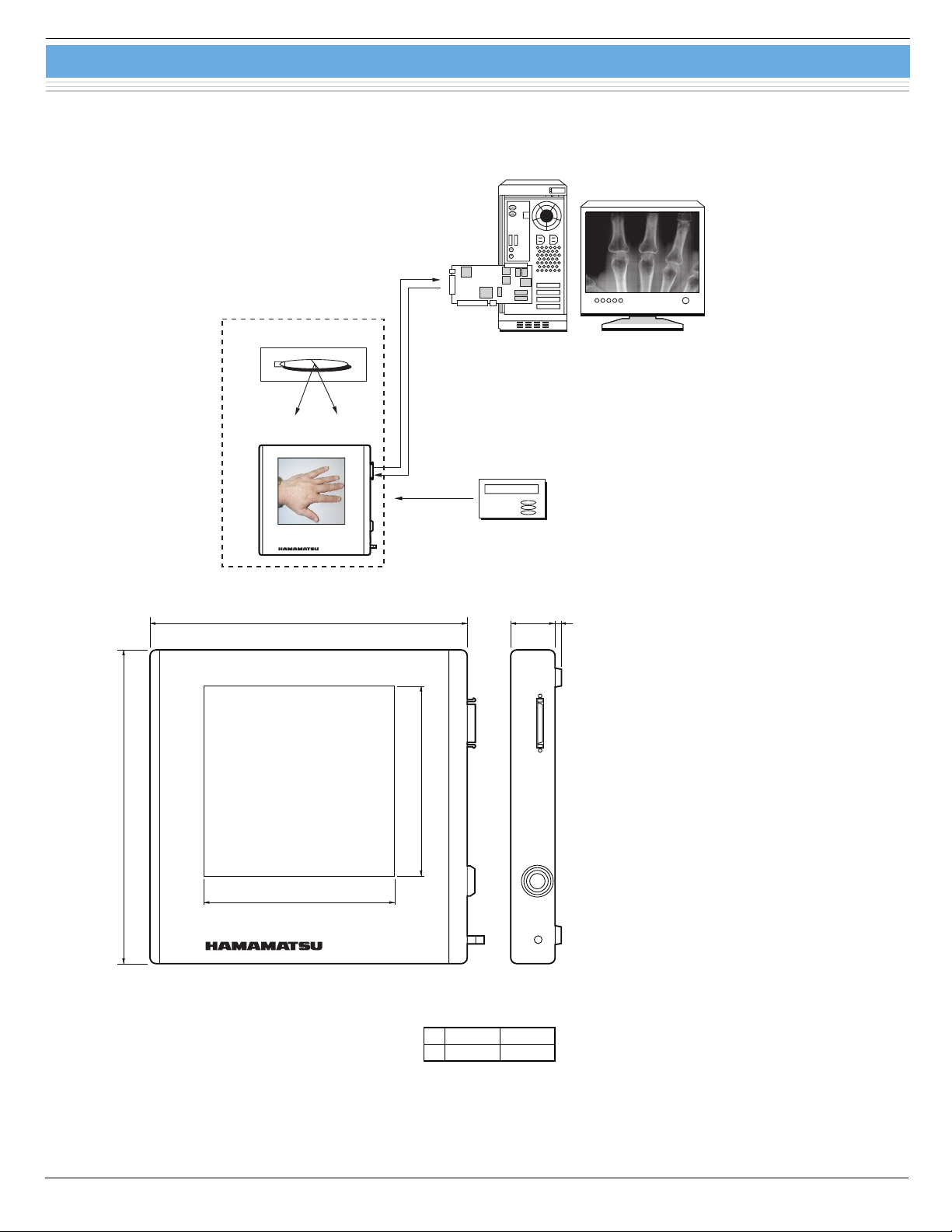
■ Connection
Install the frame grabber board into the PC by following the manufacturer’s instructions. When a general-purpose frame
grabber board i s u sed, bin nin g or tri gger operation for b in0 , bin 1, IntExt and ExtTrig can be control led with its digital I/O control.
OS +
ACQUISITION
SOFTWARE
VIDEO OUTPUT
(12 BIT DIGITAL)
Vsync, Hsync,
Pclk
(REAR VIEW)
PC/AT
GRABBER
X-RAY SOURCE
MOS Image Sensor for X-Ray
■ Dimensional outline (unit: mm)
200
BINNING
(bin0, bin1)
IntExt
ExtTrg
VOLTAGE
SOURCE
[A. Vdd, D. Vdd, V (±7.5)]
C7942CA, C7943CA
a
MONITOR
KACCC0140EA
4
28
198
a
MOS Image Sensor for X-Ray
Top cover is made of aluminum 1.0 mm thick.
C7942CA
a
120
C7943CA
124.8
KACCA0095EA
6
Page 7
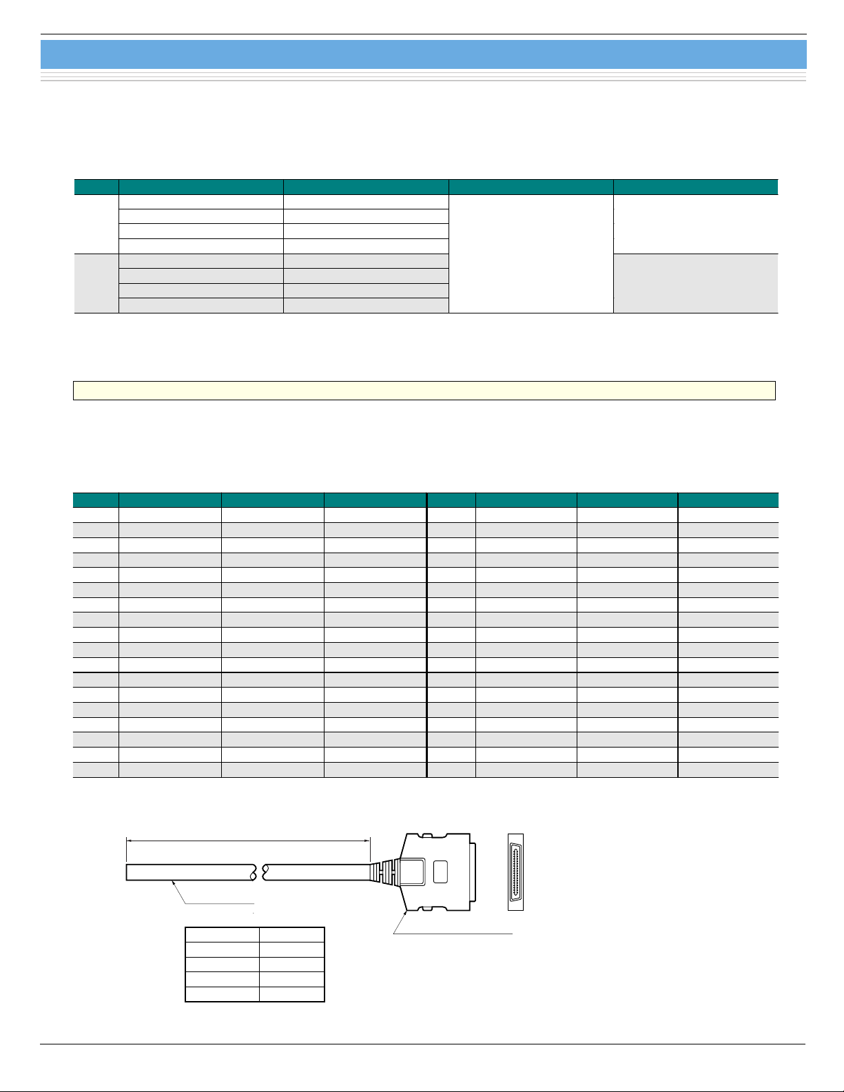
General purpose frame grabber cable
A8406-01/-06/-07/-08
Optional 36-pin cables
Two types of 36-pin cables are provided as options for connecting to the frame grabber.
Type A (A8406-01): General-purpose interface cable for digital flame grabber.
Type B (A8406-02): Interface cable for IMAQ PCI-1424 grabber board.
Typ e Cable type No. Cable length Cable end Cable end
A8406-01 5 m
A
B
*1: Made by JAE (Japan Aviation Electronics Industry, Limited)
*2: Made by Honda Tsushin Kogyo Co. Ltd.
A8406-01/-06/-07/-08 is a cable that connects the Flat Panel Sensor (C7942CA or C7943CA) to a general frame grabber. One end
of this cable has a 36-pin plug mating with the C7942CA or C7943CA digital output receptacle, but the other end is left open.
Connect the open end to a plug that mates with the frame grabber to be used. Cable color coding and specifications are shown in
the table below.
A8406-06 7 m
A8406-07 10 m
A8406-08 12 m
A8406-02 5 m
A8406-03 7 m
A8406-04 10 m
A8406-05 12 m
A8406-01/-06/-07/-08 cable for general frame grabber
TX20A-36PH1-D2P1-D1 *
open
1
PCS-XE100MA *
2
■ Cable color coding and specifications
Pin No. Signal Cable color Marking color Pin No. Signal Cable color Marking color
1 Data1+ (MSB) blue - 19 Data1- (MSB) orange -
2 Data2+ green - 20 Data2- brown 3 Data3+ gray - 21 Data3- red 4 Data4+ black - 22 Data4- yellow 5 Data5+ pink - 23 Data5- purple 6 Data6+ white - 24 Data6- blue red
7 Data7+ orange white 25 Data7- green white
8 Data8+ brown white 26 Data8- gray white
9 Data9+ red white 27 Data9- black white
10 Data10+ yellow black 28 Data10- pink black
11 Data11+ purple white 29 Data11- white blue
12 Data12+ (LSB) blue red 30 Data12- (LSB) orange white
13 bin0 (TTL) green white 31 Gnd brown white
14 bin1 (TTL) gray white 32 Gnd red white
15 ExtTrg (TTL) black white 33 IntExt (TTL) yellow black
16 Vsync+ pink black 34 Vsync- purple white
17 Hsync+ white blue 35 Hsync- blue black
18 Pclk+ orange black 36 Pclk- green black
■ Dimensional outline (unit: mm)
a
18 36
36-PIN CABLE
Cable type No.
A8406-01a5000 ± 140
A8406-06 7000 ± 140
A8406-07 10000 ± 140
A8406-08 12000 ± 140
119
TX20A-36PH1-D2P1-D1
KACCA0096EB
7
Page 8
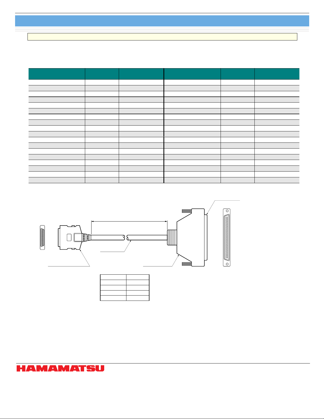
Digital frame grabber cable for IMAQ PCI-1424
A8406-02/-03/-04/-05
A8406-02/-03/-04/-05 cable for IMAQ PCI-1424 frame grabber
A8406-02/-03/-04/-05 cable is designed to connect the Flat Panel Sensor (C7942CA or C7943CA) to the National Instrument IMAQ
PCI-1424 (NI parts No. 777662-01) digital frame grabber board. Both ends of this cable have connectors. One end is a 36-pin plug
mating with the C7942CA or C7943CA digital output receptacle, while the other end is a 100-pin plug for the IMAQ PCI-1424.
■ Pin connection for A8406-02
TX20A-36PH1-D2P1-D1
Pin No.
1 Data1+ (MSB) 23 19 Data1- (MSB) 24
2 Data2+ 21 20 Data2- 22
3 Data3+ 19 21 Data3- 20
4 Data4+ 17 22 Data4- 18
5 Data5+ 15 23 Data5- 16
6 Data6+ 13 24 Data6- 14
7 Data7+ 11 25 Data7- 12
8 Data8+ 9 26 Data8- 10
9 Data9+ 7 27 Data9- 8
10 Data10+ 5 28 Data10- 6
11 Da ta11+ 3 29 D ata11- 4
12 Data12+ (LSB) 1 30 Data12- (LSB) 2
13 bin0 (TTL) 33 31 Gnd 99
14 bin1 (TTL) 35 32 Gnd 100
15 ExtTrg (TTL) 37 33 IntExt (TTL) 39
16 Vsync+ 41 34 Vsync- 42
17 Hsync+ 43 35 Hsync- 44
18 Pclk+ 49 36 Pclk- 50
Signal
PCS-XE100MA
Pin No.
TX20A-36PH1-D2P1-D1
Pin No.
Signal
PCS-XE100MA
Pin No.
■ Dimensional outline (unit: mm)
PCS-XE100MA
51
a
36
11819
TX20A-36PH1-D2P1-D1
36-PIN CABLE
100
PCS-XEM100LU2
Cable type No.
A8406-02a5000 ± 140
A8406-03 7000 ± 140
A8406-04 10000 ± 140
A8406-05 12000 ± 140
Notice) · Do not subject the Flat Panel Sensors to strong vibration or shock. (Strong shock such as drop impacts may cause
permanent damage to these sensors.)
· Users must take responsibility for implementing X-ray shielding safety measures to avoid the risk of X-ray exposure.
· This product was not designed and manufactured for use as a medical X-ray device. System manufacturers must take
responsibility for obtaining MHW or FDA approval when incorporating this product into a medical diagnostics system.
· This product is warranted for a period of 12 months after the date of the shipment.
The warranty is limited to make a replacement or repair of any defective material due to defects in workmanship or
materials used in manufacture. It does not cover loss or damage of the product due to natural calamity, misuse or total
radiation dose over 1 million Roentgen (80 kV) even within the warranty period.
1
50
KACCA0097EB
Information furnished by HAMAMATSU is believed to be reliable. However, no responsibility is assumed for possible inaccuracies or omissions.
HAMAMATSU PHOTONICS K.K., Solid State Division
1126-1 Ichino-cho, Hamamatsu City, 435-8558 Japan, Telephone: (81) 053-434-3311, Fax: (81) 053-434-5184, http://www.hamamatsu.com
U.S.A.: Hamamatsu Corporation: 360 Foothill Road, P.O.Box 6910, Bridgewater, N.J. 08807-0910, U.S.A., Telephone: (1) 908-231-0960, Fax: (1) 908-231-1218
Germany: Hamamatsu Photonics Deutschland GmbH: Arzbergerstr. 10, D-82211 Herrsching am Ammersee, Germany, Telephone: (49) 08152-3750, Fax: (49) 08152-2658
France: Hamamatsu Photonics France S.A.R.L.: 8, Rue du Saule Trapu, Parc du Moulin de Massy, 91882 Massy Cedex, France, Telephone: 33-(1) 69 53 71 00, Fax: 33-(1) 69 53 71 10
United Kingdom: Hamamatsu Photonics UK Limited: 2 Howard Court, 10 Tewin Road, Welwyn Garden City, Hertfordshire AL7 1BW, United Kingdom, Telephone: (44) 1707-294888, Fax: (44) 1707-325777
North Europe: Hamamatsu Photonics Norden AB: Smidesvägen 12, SE-171 41 Solna, Sweden, Telephone: (46) 8-509-031-00, Fax: (46) 8-509-031-01
Italy: Hamamatsu Photonics Italia S.R.L.: Strada della Moia, 1/E, 20020 Arese, (Milano), Italy, Telephone: (39) 02-935-81-733, Fax: (39) 02-935-81-741
Specifications are subject to change without notice. No patent rights are granted to any of the circuits described herein. ©2003 Hamamatsu Photonics K.K.
8
Cat. No. KACC1056E12
Sep. 2003 DN
 Loading...