

Page 1
PSD
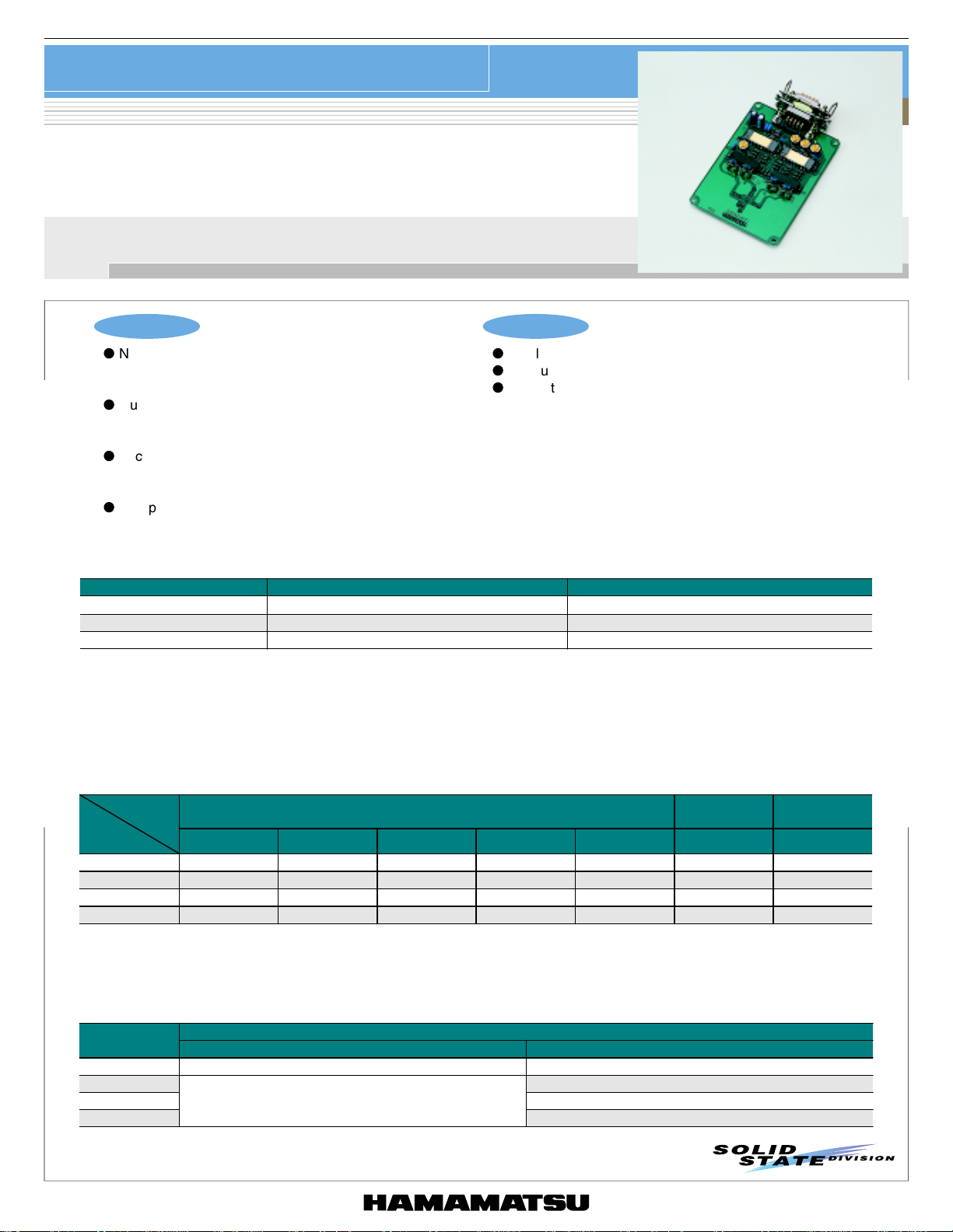
Signal processing circuit for 2-D PSD
C4674, C4757, C4758, C7563
Signal processing circuit designed to facilitate operation of 2-D Position Sensitive Detector
Features
l
No complicated adjustment required
Position measurement can be made simply by mounting
2-D PSD.
l
Output voltage directly representing the position data
The position (mm) of a light spot from the PSD center is
obtained as an output voltage (V).
l
Accurate position detection
Accurate position data can be obtained, independent of
light intensity.
l
Compact on-board configuration
A head amplifiers, signal addition/subtraction circuits, and
analog divider are mounted on a compact PC board.
Applications
l
Displacement measurements using 2-D PSD
l
Various studies using 2-D PSD
l
Evaluation of 2-D PSD
■ Four models are available to meet various 2-D PSD types
PSD type DC signal processing circuit AC signal processing circuit
Pin-cushion type PSD C4674 C7563
Duo-lateral type PSD C4757 Tetra-lateral type PSD C4758 -
DC signal processing circuit
●
Suitable for DC light displacement measurement.
AC signal processing circuit
●
Designed specifically for pulse (AC) signal detection.
Has a synchronous circuit, S/H (sample & hold) circuit and LED driver circuit.
Use of a pulse-driven LED ensures reliable operation even under background light.
■■■■ Combination with Hamamatsu 2-D PSD
Each signal processing circuit can be used with the following Hamamatsu 2-D PSD.
PSD
Signal
processing circuit
C4674 O O
C4757 O
C4758 O
C7563 O O
*1: Connected externally
*2: Using attachment board
S1880 S1881 S2044 S5990-01 S5991-01 S1300 S1200
Pin-cushion type
*1
*1
OO *2O
O O
*2
O
*2
*2
Duo-lateral
type
Tetra-lateral
type
■■■■ Accessories
The mating connectors to a power supply/signal readout device and the boards for mounting surface-mounting ceramic
package PSD are supplied with each signal processing circuit.
Type No.
C4674 HDEB-9S (made by Hirose Electric) for mounting S5990-01, S5991-01
C4757 -
C4758 -
C7563
HDAB-15S (made by Hirose Electric)
Supplied connector Attachment board
Accessory
for mounting S5990-01, S5991-01
1
Page 2
Signal processing circuit for 2-D PSD
■ Absolute maximum ratings
Parameter Symbol
Supply voltage Vcc Max. ±18 V
Signal
processor
LED driver
Input current IIN Max. Vcc Max. × 10
Output short-circuit time - Continuous s
Operating temperature Topr 0 to +50
Transistor collector-emitter voltage V
Transistor collector current *
Transistor collector dissipation *
C4674, C4757, C4758, C7563
DC circuit
C4674 C4757 C4758 C7563
3
3
CE
C
I
Pc - - - 900 mW
-- -+50V
- - - 2 A
AC circuit
-5
Unit
A
°
C
■ Specifications (Ta=25
°
C, Vcc=
15 V)
±
Typical value
AC circuit
Unit
V/A
-4
A
4
Symbol
Rf
Parameter
Head-amp conversion impedance *
Feedback capacitance Cf
Input signal current *
5
I
Condition
Factory setup prior to shipping
Factory setup prior to shipping
Photocurrent with PSD
IN
installed
DC circuit
C4674 C4757 C4758 C7563
1 × 10
5
100 22 pF
-5
1 × 10
to 1 × 10
Output response time
versus movement of light
spot position, measured
with PSD installed.
7
OS
*
With PSD installed and
Vo
light spot falling on edge
of active area.
All range *
Vn
7
3
Ic *
8
30 µs
-10 to +10 mV
-10 to +10 V
7
5 10 mVp-p
±15 ±60 mA
- - - 680 mAp-p
- - - 333 HzLED
Open
collector
-
Signal
processor
driver
Rise time tr
PSD reverse bias voltage VR-+5V
Output offset voltage V
Output voltage amplitude *
6
Output noise (analog divider)
Current consumption Icc *
Transistor collector current
Repetition frequency fT*
Output type - - - - -
*3: Duty ratio: 3/100, pulse width: 90 µs, LED: Hamamatsu L1915-01 (sold separately)
*4: These resistors are lead types and inserted into sockets, so it can be easily to exchange by the user if necessary in a range
between 1 × 10
4
to 1 × 10⁶ Ω. For more details, see the instruction manual that comes with the product.
*5: The circuit does not operate correctly when input signal level is not appropriate.
*6: Maximum output amplitude can be adjusted in a range of ±2 to ±10 V according to PSD type to be used.
*7: Measured without PSD and with LED turned off, while using a current source of 20 µA (X1=X2=Y1=Y2) substituting for PSD
photocurrent. In the case of C7563, however, pulse current with a duty ratio of 3/100 and a pulse width of 90 µs is supplied.
*8: Repetition frequency 333 Hz (duty ratio: 3/100, pulse width: 90 µs) cannot be modulated.
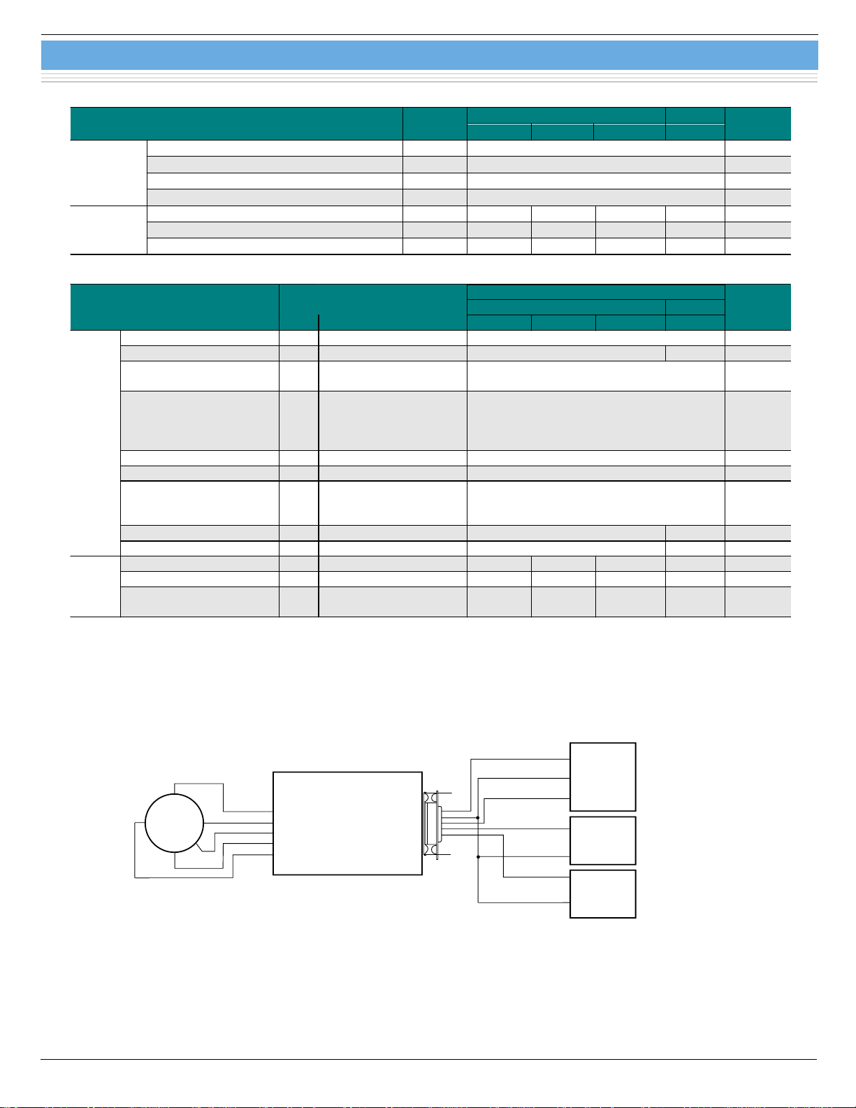
■ Operating example (C4674)
2-D
PSD
Y
X2
VR
Y1
X1
2
SIGNAL
PROCESSING CIRCUIT
C4674
3
5
4
1
2
+V
GND
-V
Xout
GND
Yout
+15 V
0 V
-15 V
REGULATED
POWER
SUPPLY *
+
VOLTMETER
-
+
GND
Constant voltage power supply: ±15 V, Power capacity: 0.1 A Min.
Ripple voltage: 3 mVp-p Max.
-
VOLTMETER
KPSDC0034ED
Condition
1. Light source LED (λ=900 nm)
2. Light spot diameter φ200 µm
The followings are obtained with the conditions listed
on the left.
3. PSD used S1880 (12 × 12 mm)
4. PSD photocurrent 10 µA
5. Signal processing circuit C4674
6. Frequency bandwidth 10 Hz
7. Voltmeter KEITHLEY model 195 A
Output voltage amplitude V
Position resolution ∆x=0.1 µm approx.
(calculated values) ∆y=0.1 µm approx.
FS (X)=±6 V
FS (Y)=±6 V
V
2
Page 3
Signal processing circuit for 2-D PSD
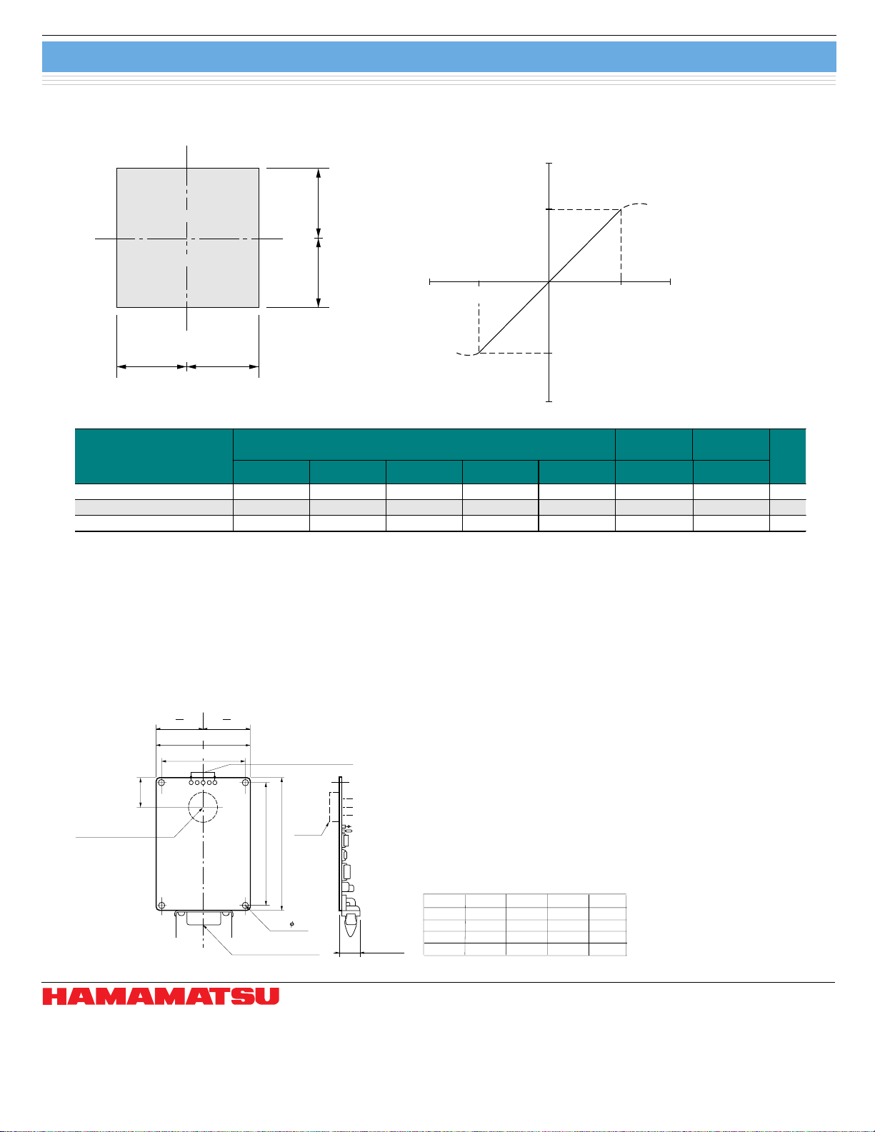
■ 2-D PSD and output voltage
Y
2
ACTIVE AREA
1
X
L × L mm
C4674, C4757, C4758, C7563
OUTPUT VOLTAGE (Xout or Yout)
+L/2
X
0
2
(V)
+L/2
-L/2
Y
1
-L/2
0
-L/2
+L/2
POSITION OF LIGHT SPOT
(mm)
0 +L/2-L/2
KPSDC0032EB KPSDC0033EA
Parameter
S1880 S1881 *
Pin-cushion type
9
S2044 S5990-01 S5991-01 S1300 S1200
Duo-lateral
type
Tetra-lateral
type
Unit
Active area length L 12 22 4.7 4 9 13 13 mm
Output voltage am plitude Vo (X)
Output voltage am plitude Vo (Y)
±6 ±5.5 ±2.35 ±2 ±4.5 ±6.5 ±6.5 V
±6 ±5.5 ±2.35 ±2 ±4.5 ±6.5 ±6.5 V
*9: The position (mm) of light spot from the center is twice the output voltage (V) for the S1881.
If the incident light spot is not sufficiently focused on the PSD, i.e., the light spot diameter is large, and falls upon near the edge
of the active area, part of the light spot may go outside the active area, thus degrading position accuracy.
The output voltage amplitude values listed above are measured when the light spot diameter is made as small as possible within
the range in which adequate intensity is maintained.
■ Dimensional outline (unit: mm, tolerance: ±0.2 mm)
b
2
20
CENTER OF
MOUNTED PSD
HAMAMATSU PHOTONICS K.K., Solid State Division
1126-1 Ichino-cho, Hamamatsu City, 435-8558 Japan, Telephone: (81) 053-434-3311, Fax: (81) 053-434-5184, http://www.hamamatsu.com
U.S.A.: Hamamatsu Corporation: 360 Foothill Road, P.O.Box 6910, Bridgewater, N.J. 08807-0910, U.S.A., Telephone: (1) 908-231-0960, Fax: (1) 908-231-1218
Germany: Hamamatsu Photonics Deutschland GmbH: Arzbergerstr. 10, D-82211 Herrsching am Ammersee, Germany, Telephone: (49) 08152-3750, Fax: (49) 08152-2658
France: Hamamatsu Photonics France S.A.R.L.: 8, Rue du Saule Trapu, Parc du Moulin de Massy, 91882 Massy Cedex, France, Telephone: 33-(1) 69 53 71 00, Fax: 33-(1) 69 53 71 10
United Kingdom: Hamamatsu Photonics UK Limited: 2 Howard Court, 10 Tewin Road, Welwyn Garden City, Hertfordshire AL7 1BW, United Kingdom, Telephone: (44) 1707-294888, Fax: (44) 1707-325777
North Europe: Hamamatsu Photonics Norden AB: Smidesvägen 12, SE-171 41 Solna, Sweden, Telephone: (46) 8-509-031-00, Fax: (46) 8-509-031-01
Italy: Hamamatsu Photonics Italia S.R.L.: Strada della Moia, 1/E, 20020 Arese, (Milano), Italy, Telephone: (39) 02-935-81-733, Fax: (39) 02-935-81-741
b
2
b
d
D-SUB CONNECTOR
THROUGH HOLES
FOR EXTERNALLY
CONNECTED PSD
PSD *
c
a
Symbol
(4 ×) 3.2
15.5 MAX.
* PSD is not mounted on this board.
Information furnished by HAMAMATSU is believed to be reliable. However, no responsibility is assumed for possible inaccuracies or omissions.
Specifications are subject to change without notice. No patent rights are granted to any of the circuits described herein. ©2003 Hamamatsu Photonics K.K.
C4674
a
b
c
d
C4757
90
92
65
70
84
84
59
62
C4758
90
65
83
57
C7563
110
75
102
67
KPSDA0018EC
Cat. No. KPSD1005E06
Apr. 2003 DN
3
 Loading...