

Page 1
PHOTODIODE
16 × 16 element photodiode array detector
C4675 series
2-D detector using 256-element photodiode with visible sensitivity
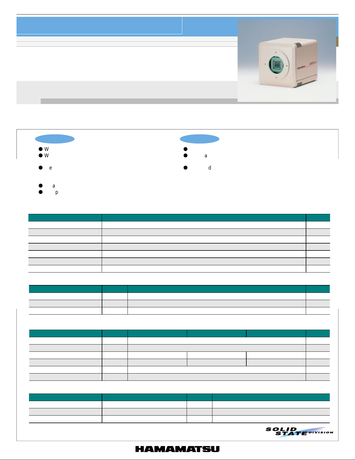
C4675 series is a two-dimensional detector using a 16 × 16 (256) element Si PIN photodiode array that has high sensitivity in the visible range.
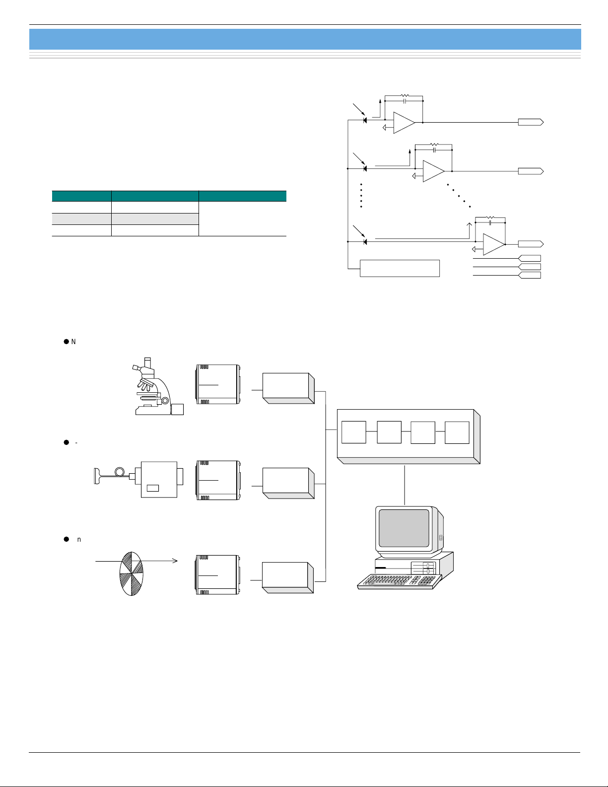
Current-to-voltage conversion amplifiers in the signal amplifier section are connected in parallel to each element of the photodiode array, thereby
allowing high-speed parallel signal processing.
C4675 series is also designed to suppress the power consumption so it operates from two power supplies (±15 V).
Features
l
Wide spectral response: 400 to 1000 nm
l
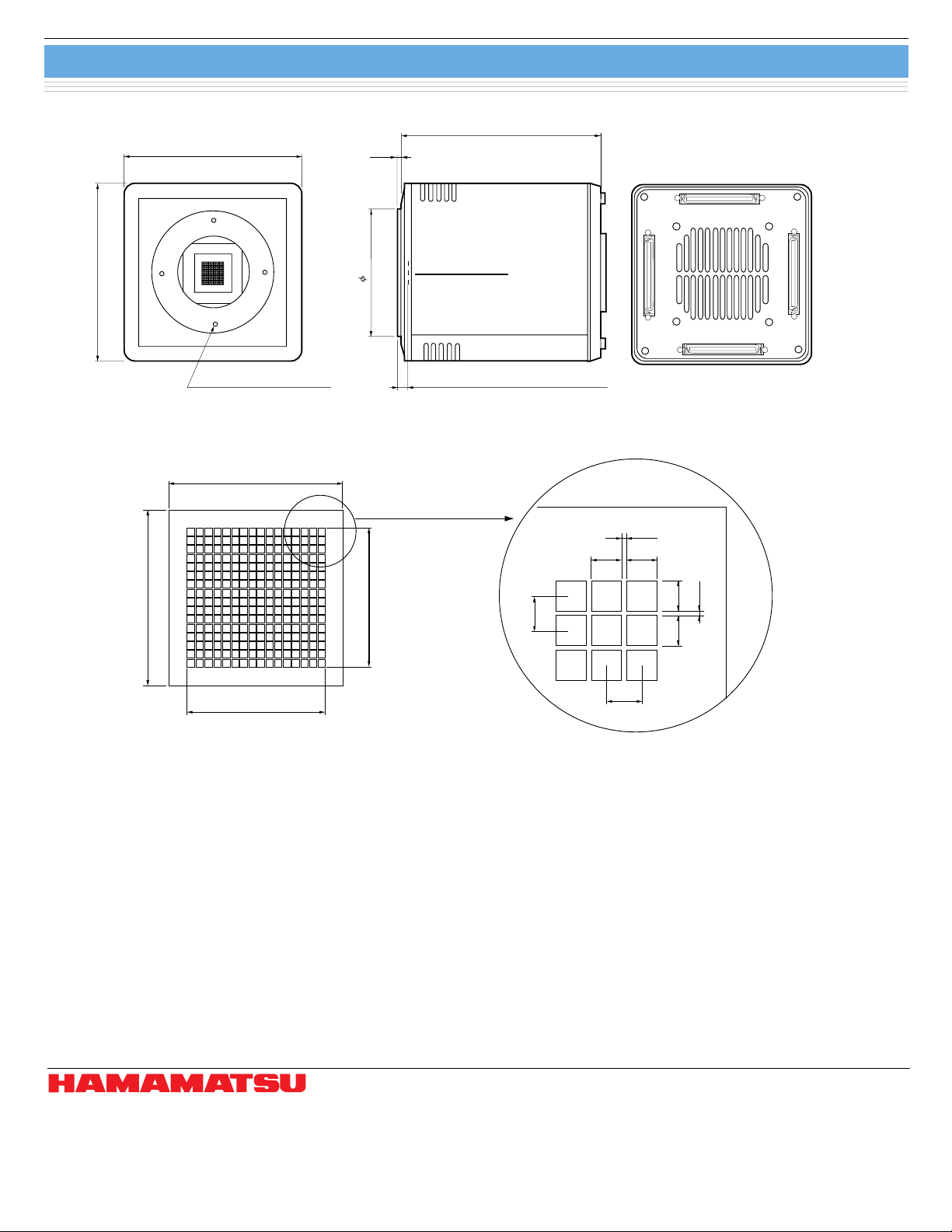
Wide active area: 17.45 × 17.45 mm
(0.95 × 0.95 mm per element, 1.1 mm pitch)
l
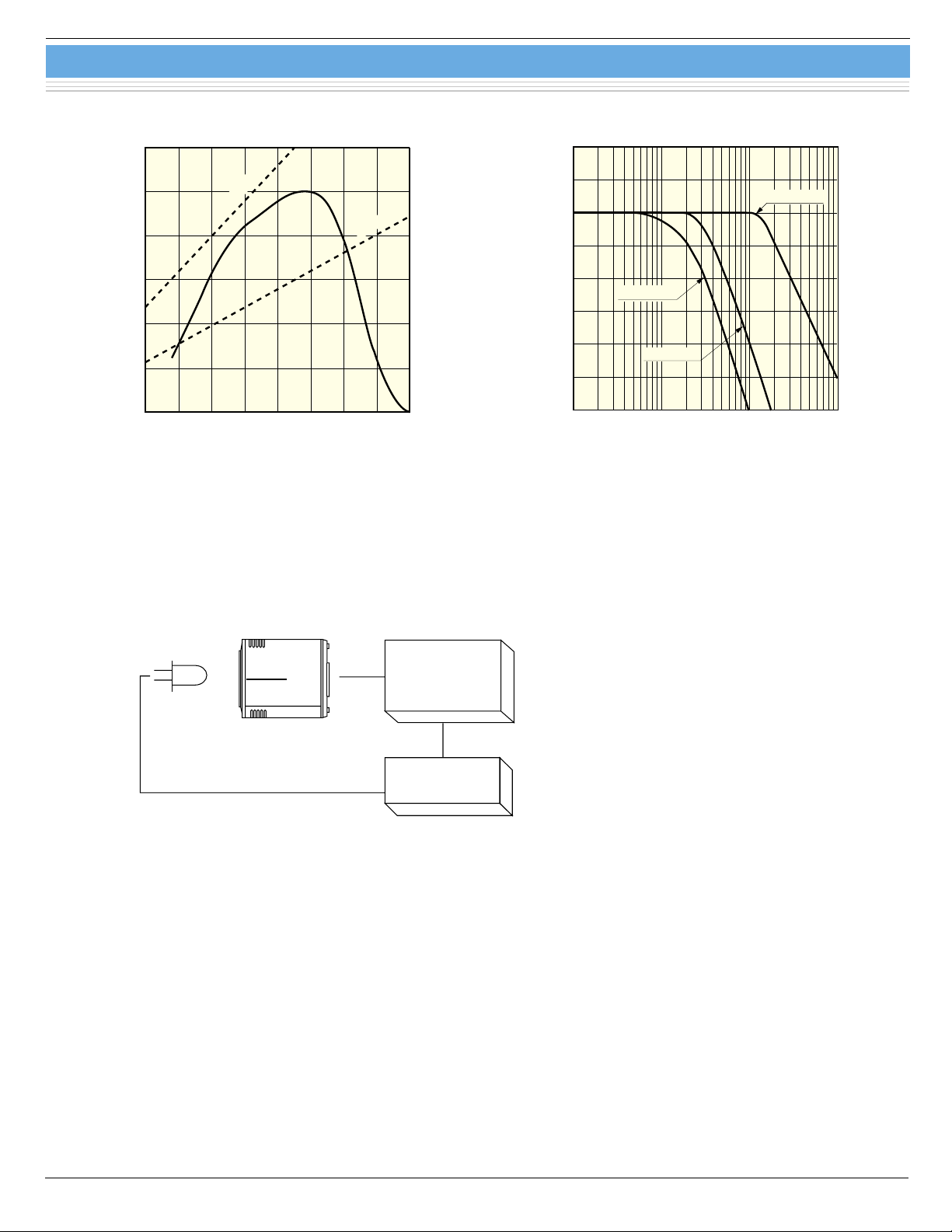
Frequency response C4675-102: DC to 1 kHz
l
Parallel signal output by current-to-voltage amplifier
l
Low power consumption: 2.5 W Typ.
■
General ratings
Parameter Rating Unit
Photodiode Si PIN photodiode array (Made by Hamamatsu S4529) Number of element 16 × 16 (256) Active area (per 1 element) 0.95 × 0.95 mm
Element pitch 1.1 mm
Output type Current-to-voltage conversion method, 256-ch parallel analog voltage output Dimensional outline 136 (W) × 136 (H) × 153.5 (D) mm
Weight 2.1 kg
■
Absolute maximum ratings
Parameter Symbol Value Unit
Operating temperature Topr 0 to +50 °C
Storage temperature Tstg -10 to +60 (no condensation) °C
Supply voltage Vs ±18 V
C4675-302: DC to 3 kHz
C4675-103: DC to 10 kHz
Applications
l
Nerve potential measurement under microscope
l
2-D (wavelength × spatial position) spectrophotometry
in visible range
l
Fine-modulation light measurement
■
Electrical and optical characteristics (Typ. Ta=25 °C)
Parameter Symbol C4675-102 C4675-302 C4675-103 Unit
Spectral response range
Output uniformity - ±15 %
Amp gain - 10
Frequency response - DC to 1 k DC to 3 k DC to 10 k Hz
Supply voltage Vs ±15 V
Current consumption P 2.5 W
■
Construct device
Product name Type No. Number Note
Two-dimensional detector C4675 series 1
Dedicated cable 8840S-080-174AD-150-W 4 Made by KEL, length 1.5 m
Output connector 8850-080-170SD 4 Made by KEL, on-board straight installation type
λ
8
400 to 1000 nm
5 × 10
7
10
7
V/A
Page 2
16 × 16 element photodiode array detector
C4675-xxx
C4675 series
■ Spectral response
0.6
0.5
0.4
0.3
0.2
PHOTO SENSITIVITY (A/W)
0.1
0
400
300
500
QE=100 %
600 700 800 900 1000
(Ta=25 ˚C)
QE=50 %
1100
■ F requency response
10
0
-10
C4675-102
-20
RELATIVE OUTPUT (5 dB/div.)
-30
C4675-302
10.1
(Typ. Ta=25 ˚C)
C4675-103
10 100
FREQUENCY (kHz)
WAVELENGTH (nm)
KACCB0001EA
■ Measurement method for frequency characteristics
The LED output was adjusted so that the output voltage Vo from C4675 series is set to 5 V. Under this condition, the output of
C4675 series was monitored by FFT while sweeping the LED drive frequencies.
KACCB0002EB
LED
HAMAMATSU
C4675-xxx
Vo
FFT
SWEEP
GENERATOR
KACCC0002EA
Page 3
16 × 16 element photodiode array detector
LOW NOISE BIAS CIRCUIT
+15 V
GND
-15 V
CH 1
CH 2
INCIDENT LIGHT
Ip
Rf
Cf (1p)
-15 V
GND
+15 V
CH256
Rf
Ip
Cf (1p)
Rf
Ip
Cf (1p)
-
+
-
+
-
+
C4675-xxx
C4675-xxx
C4675-xxx
C4675 series
■ Operating principle
When light enters a photodiode, photoelectric conversion
occurs in the photodiode and the photocurrent Ip is generated. The photocurrent Ip then flows through the current-tovoltage conversion amplifier feedback resistance Rf and is
output as voltage V (=Ip × Rf).
C4675 series uses current-to-voltage conversion amplifiers
connected to each of the 256-element photodiodes to perform parallel signal processing. A low noise bias circuit is
also used to reduce the photodiode junction capacitance.
Type No.
C4675-102
C4675-302
C4675-103
Feedback resistance Feedback capacitance
100 M
Ω
50 M
10 M
Ω
Ω
1 pF
■ Application example
l
Nerve potential measurement under microscope
■ Block diagram
KACCC0001EA
l
2-D spectrophotometry in visible range
FIBER
SPECTRUM
RECEPTACLE
l
Fine-modulation light measurement
CHOPPER
HAMAMATSU
HAMAMATSU
HAMAMATSU
C4675-xxx
C4675-xxx
C4675-xxx
AC
GAIN AMP
GAIN AMP
LOCK IN AMP
DATA PROCESSING DEVICE
SH
MUX ADC
MEMORY
KACCC0003EA
Page 4
16 × 16 element photodiode array detector
C4675 series
■ Dimensional outline (unit: mm)
136
136
PCD80 (4 ×) M3 DEPTH 4
22.0
94
151
2.5
HAMAMATSU
C4675-xxx
7.1 (POSITION OF PHOTOSENSITIVE SURFACE)
0.95
+
×
CN. 4
+
+
×
CN1 TO CN4
(MADE BY KEL 8850-080-170L)
CN. 1
+
+
CN. 3
+
0.15
0.95
+
×
CN. 2
+
+
+
+
×
+
KACCA0001EA
22.0
0.15
17.45
0.95
1.10
0.95
1.10
17.45
DETAILS
DETAILS OF ACTIVE AREA (16 × 16 element photodiode array S4529)
KACCA0002EA
Information furnished by HAMAMATSU is believed to be reliable. However, no responsibility is assumed for possible inaccuracies or omissions.
Specifications are subject to change without notice. No patent rights are granted to any of the circuits described herein. ©2001 Hamamatsu Photonics K.K.
HAMAMATSU PHOTONICS K.K., Solid State Division
1126-1 Ichino-cho, Hamamatsu City, 435-8558 Japan, Telephone: (81) 053-434-3311, Fax: (81) 053-434-5184, http://www.hamamatsu.com
U.S.A.: Hamamatsu Corporation: 360 Foothill Road, P.O.Box 6910, Bridgewater, N.J. 08807-0910, U.S.A., Telephone: (1) 908-231-0960, Fax: (1) 908-231-1218
Germany: Hamamatsu Photonics Deutschland GmbH: Arzbergerstr. 10, D-82211 Herrsching am Ammersee, Germany, Telephone: (49) 08152-3750, Fax: (49) 08152-2658
France: Hamamatsu Photonics France S.A.R.L.: 8, Rue du Saule Trapu, Parc du Moulin de Massy, 91882 Massy Cedex, France, Telephone: 33-(1) 69 53 71 00, Fax: 33-(1) 69 53 71 10
United Kingdom: Hamamatsu Photonics UK Limited: 2 Howard Court, 10 Tewin Road, Welwyn Garden City, Hertfordshire AL7 1BW, United Kingdom, Telephone: (44) 1707-294888, Fax: (44) 1707-325777
North Europe: Hamamatsu Photonics Norden AB: Smidesvägen 12, SE-171 41 Solna, Sweden, Telephone: (46) 8-509-031-00, Fax: (46) 8-509-031-01
Italy: Hamamatsu Photonics Italia S.R.L.: Strada della Moia, 1/E, 20020 Arese, (Milano), Italy, Telephone: (39) 02-935-81-733, Fax: (39) 02-935-81-741
Cat. No. KACC1001E02
Apr. 2001 DN
 Loading...