

Page 1
DISCRETE SEMICONDUCTORS
DATA SH EET
dbook, halfpage
M3D184
BZA109
9-fold ESD transient voltage
suppressor
Product specification
Supersedes data of 1997 Oct 27
File under Discrete Semiconductors, SC01
1997 Dec 01
Page 2
Philips Semiconductors Product specification
9-fold ESD transient voltage suppressor BZA109
FEATURES
• ESD rating >8 kV, according to
IEC1000-4-2
• SOT163-1 surface mount package
• Common anode configuration
• Non-clamping range 0.5 to 6.8 V
• Maximum non-repetitive peak
reverse power dissipation: 25 W
at tp=1ms
• Maximum clamping voltage at peak
pulse current: 10 V at I
ZSM
= 2.5 A.
APPLICATIONS
• For 9-bit wide undershoot/
overshoot clamping and fast ESD
transient suppression in:
– Computers and peripherals
– Audio and video equipment
– Business machines
– Communication systems
– Medical equipment.
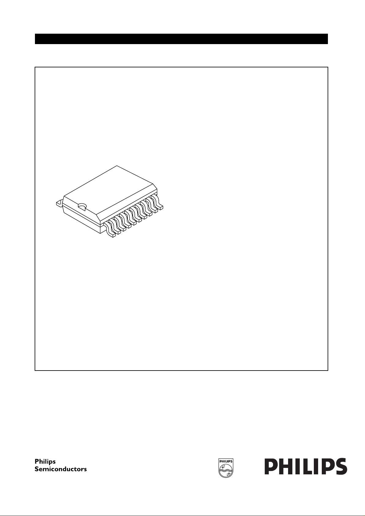
DESCRIPTION
9-fold monolithic transient voltage
suppressor in an SO20; SOT163-1
surface mount package. The device is
ideal in situations where board space
is a premium.
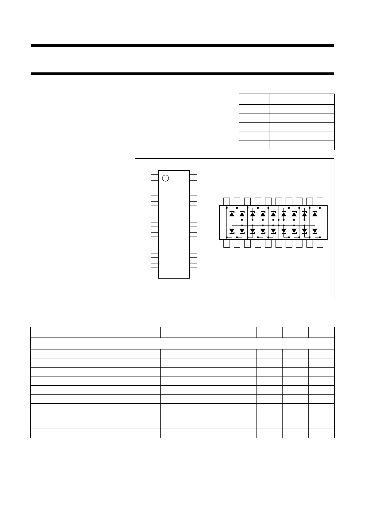
handbook, 4 columns
1
2
3
4
5
6
7
8
9
10
SO20
OUT1IN1
20
OUT2IN2
19
OUT3IN3
18
OUT4IN4
17
OUT5IN5
16
GNDGND
15
14
OUT6IN6
13
OUT7IN7
12
OUT8IN8
11
OUT9IN9
PINNING
PIN DESCRIPTION
1 to 5 input (IN1 to IN5)
6 and 15 common anode (GND)
7 to 10 input (IN6 to IN9)
11 to 14 output (OUT9 to OUT6)
16 to 20 output (OUT5 to OUT1)
19 18 17 16 15 14 13 12 1120
2 3 4 5 6 7 8 9 101
MBK268
Fig.1 Pin configuration for SO20 (SOT163-1) and symbol.
LIMITING VALUES
In accordance with the Absolute Maximum Rating System (IEC 134).
SYMBOL PARAMETER CONDITIONS MIN. MAX. UNIT
Per diode
I
Z
I
F
I
FT
I
FSM
I
ZSM
P
P
tot
ZSM
working current T
continuous forward current T
feed-through current T
non-repetitive peak forward current tp= 1 ms; square pulse − 4.5 A
non-repetitive peak reverse current tp= 1 ms; square pulse; see Fig.2 − 2.5 A
total power dissipation T
non-repetitive peak reverse power
=25°C − 20 mA
amb
=25°C − 100 mA
amb
=25°C; note 1 − 100 mA
amb
≤ 25 °C; note 2; see Fig.3 − 1.25 W
amb
tp= 1 ms; square pulse; see Fig.4 − 25 W
dissipation
T
stg
T
j
storage temperature −65 +150 °C
operating junction temperature −65 +150 °C
Notes
1. Current is flowing from input to corresponding output.
2. One or more diodes loaded.
1997 Dec 01 2
Page 3

Philips Semiconductors Product specification
9-fold ESD transient voltage suppressor BZA109
THERMAL CHARACTERISTICS
SYMBOL PARAMETER CONDITIONS VALUE UNIT
R
th j-a
ELECTRICAL CHARACTERISTICS
=25°C unless otherwise specified.
T
j
SYMBOL PARAMETER CONDITIONS MIN. TYP. MAX. UNIT
Per diode
V
Z
V
F
V
ZSM
I
H
r
dif
S
Z
C
d
thermal resistance from junction to ambient one or more diodes loaded 100 K/W
working voltage IZ = 250 µA 6.4 6.8 7.2 V
forward voltage IF= 100 mA −−1.1 V
non-repetitive peak reverse voltage I
= 2.5 A; tp=1ms −−10 V
ZSM
input high current VIN= 5.25 V −−0.5 µA
differential resistance IZ= 250 µA −−100 Ω
temperature coefficient of
IZ=5mA − 3 − mV/K
working voltage
diode capacitance see Fig.5
V
= 0; f = 1 MHz −−200 pF
R
V
= 5.25 V; f = 1 MHz −−100 pF
R
1997 Dec 01 3
Page 4
Philips Semiconductors Product specification
9-fold ESD transient voltage suppressor BZA109
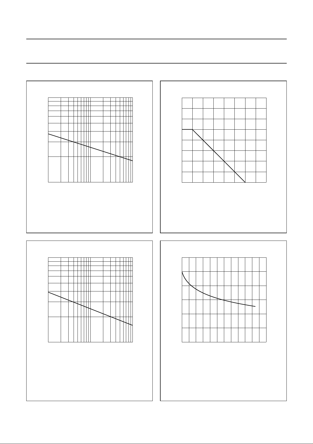
GRAPHICAL DATA
10
handbook, halfpage
I
ZSM
(A)
1
−1
10
110
t
(ms)
p
Fig.2 Maximum non-repetitive peak reverse
current as a function of pulse time.
MBK269
2.0
handbook, halfpage
P
tot
(W)
1.5
1.0
0.5
0
050
One or more diodes loaded.
Fig.3 Power derating curve.
MBK393
100 200
150
T
amb
(°C)
2
10
handbook, halfpage
P
ZSM
(W)
10
−1
10
P
ZSM=VZSM
V
ZSM
× I
.
is the non-repetitive peak reverse voltage at I
ZSM
110
t
MBK270
(ms)
p
.
ZSM
Fig.4 Maximum non-repetitive peak reverse power
dissipation as a function of pulse duration
(square pulse).
150
handbook, halfpage
C
d
(pF)
100
50
0
0
Tj=25°C; f = 1 MHz.
26
4
MBK272
V
(V)
R
Fig.5 Diode capacitance as a function of reverse
voltage; typical values.
1997 Dec 01 4
Page 5

Philips Semiconductors Product specification
9-fold ESD transient voltage suppressor BZA109
handbook, full pagewidth
IEC 1000-4-2 network
CZ = 150 pF; RZ = 330 Ω
ESD TESTER
R
Z
C
Z
450 Ω
450 Ω
input output
1/9 BZA109
vertical scale = 100 V/Div
horizontal scale = 50 ns/Div
RG 223/U
50 Ω coax
RG 223/U
50 Ω coax
10×
ATTENUATOR
note 1
10×
ATTENUATOR
note 1
Note 1: attenuator is only used for open
socket high voltage measurements
vertical scale = 10 V/Div
horizontal scale = 50 ns/Div
GND
output
OSCILLOSCOPE
OSCILLOSCOPE
DIGITIZING
CH1
50 Ω
DIGITIZING
CH2
50 Ω
GND
unclamped +1 kV ESD voltage waveform
(IEC1000−4−2 network)
GND
vertical scale = 100 V/Div
horizontal scale = 50 ns/Div
unclamped −1 kV ESD voltage waveform
(IEC1000−4−2 network)
Fig.6 ESD clamping test set-up and waveforms.
GND
clamped +1 kV ESD voltage waveform
(IEC1000−4−2 network)
GND
GND
clamped −1 kV ESD voltage waveform
(IEC1000−4−2 network)
input
vertical scale = 10 V/Div
horizontal scale = 50 ns/Div
input
output
MBK273
1997 Dec 01 5
Page 6

Philips Semiconductors Product specification
9-fold ESD transient voltage suppressor BZA109
APPLICATION INFORMATION
Typical common anode application
A 9-fold transient suppressor in an SO20; SOT163-1 package makes it possible to protect nine separate lines using only
one package. Two simplified examples are shown in Figs 7 and 8.
handbook, full pagewidth
keyboard,
terminal,
printer,
etc.
handbook, full pagewidth
I/O
BZA109
Fig.7 Computer interface protection.
address bus
FUNCTIONAL
DECODER
A
B
C
D
E
F
G
H
I
MBK274
GND
V
DD
V
GG
RAM
I/O
4/9 BZA109
Fig.8 Microprocessor protection.
1997 Dec 01 6
data bus
control bus
ROM
CPU
CLOCK
MBK275
GND
Page 7

Philips Semiconductors Product specification
9-fold ESD transient voltage suppressor BZA109
Device placement and printed-circuit board layout
Circuit board layout is of extreme importance in the suppression of transients. The clamping voltage of the BZA109 is
determined by the peak transient current and the rate of rise of that current (di/dt). Since parasitic inductances can further
add to the clamping voltage (V = L di/dt) the series conductor lengths on the printed-circuit board should be kept to a
minimum. This includes the lead length of the suppression element.
In addition to minimizing conductor length the following printed-circuit board layout guidelines are recommended:
1. Place the suppression element close to the input terminals or connectors.
2. Keep parallel signal paths to a minimum.
3. Avoid running protection conductors in parallel with unprotected conductors.
4. Minimize all printed-circuit board loop areas including power and ground loops.
5. Minimize the length of the transient return path to ground.
6. Avoid using shared transient return paths to a common ground point.
1997 Dec 01 7
Page 8

Philips Semiconductors Product specification
9-fold ESD transient voltage suppressor BZA109
PACKAGE OUTLINE
SO20: plastic small outline package; 20 leads; body width 7.5 mm
D
c
y
Z
20
pin 1 index
1
e
11
A
2
10
w M
b
p
SOT163-1
E
H
E
Q
A
1
L
p
L
detail X
(A )
A
X
v M
A
A
3
θ
0 5 10 mm
scale
DIMENSIONS (inch dimensions are derived from the original mm dimensions)
mm
OUTLINE
VERSION
SOT163-1
A
max.
2.65
0.10
A
1
0.30
0.10
0.012
0.004
A2A
2.45
2.25
0.096
0.089
IEC JEDEC EIAJ
075E04 MS-013AC
0.25
0.01
b
3
p
0.49
0.32
0.36
0.23
0.019
0.013
0.014
0.009
UNIT
inches
Note
1. Plastic or metal protrusions of 0.15 mm maximum per side are not included.
(1)E(1) (1)
cD
13.0
7.6
7.4
0.30
0.29
1.27
0.050
12.6
0.51
0.49
REFERENCES
1997 Dec 01 8
eHELLpQ
10.65
10.00
0.419
0.394
1.4
0.055
1.1
0.4
0.043
0.016
1.1
1.0
0.043
0.039
PROJECTION
0.25
0.25 0.1
0.01
0.01
EUROPEAN
ywv θ
Z
0.9
0.4
8
0.004
ISSUE DATE
0.035
0.016
95-01-24
97-05-22
0
o
o
Page 9

Philips Semiconductors Product specification
9-fold ESD transient voltage suppressor BZA109
DEFINITIONS
Data Sheet Status
Objective specification This data sheet contains target or goal specifications for product development.
Preliminary specification This data sheet contains preliminary data; supplementary data may be published later.
Product specification This data sheet contains final product specifications.
Limiting values
Limiting values given are in accordance with the Absolute Maximum Rating System (IEC 134). Stress above one or
more of the limiting values may cause permanent damage to the device. These are stress ratings only and operation
of the device at these or at any other conditions above those given in the Characteristics sections of the specification
is not implied. Exposure to limiting values for extended periods may affect device reliability.
Application information
Where application information is given, it is advisory and does not form part of the specification.
LIFE SUPPORT APPLICATIONS
These products are not designed for use in life support appliances, devices, or systems where malfunction of these
products can reasonably be expected to result in personal injury. Philips customers using or selling these products for
use in such applications do so at their own risk and agree to fully indemnify Philips for any damages resulting from such
improper use or sale.
1997 Dec 01 9
Page 10

Philips Semiconductors Product specification
9-fold ESD transient voltage suppressor BZA109
NOTES
1997 Dec 01 10
Page 11

Philips Semiconductors Product specification
9-fold ESD transient voltage suppressor BZA109
NOTES
1997 Dec 01 11
Page 12

Philips Semiconductors – a worldwide company
Argentina: see South America
Australia: 34 Waterloo Road, NORTH RYDE, NSW 2113,
Tel. +61 2 9805 4455, Fax. +61 2 9805 4466
Austria: Computerstr. 6, A-1101 WIEN, P.O. Box 213, Tel. +43 160 1010,
Fax. +43 160 101 1210
Belarus: Hotel Minsk Business Center, Bld. 3, r. 1211, Volodarski Str. 6,
220050 MINSK, Tel. +375 172 200 733, Fax. +375 172 200 773
Belgium: see The Netherlands
Brazil: seeSouth America
Bulgaria: Philips Bulgaria Ltd., Energoproject, 15thfloor,
51 James Bourchier Blvd., 1407 SOFIA,
Tel. +359 2 689 211, Fax. +359 2 689 102
Canada: PHILIPS SEMICONDUCTORS/COMPONENTS,
Tel. +1 800 234 7381
China/Hong Kong: 501 Hong Kong Industrial Technology Centre,
72 Tat Chee Avenue, Kowloon Tong, HONG KONG,
Tel. +852 2319 7888, Fax. +852 2319 7700
Colombia: see South America
Czech Republic: see Austria
Denmark: Prags Boulevard 80, PB 1919, DK-2300 COPENHAGEN S,
Tel. +45 32 88 2636, Fax. +45 31 57 0044
Finland: Sinikalliontie 3, FIN-02630 ESPOO,
Tel. +358 9 615800, Fax. +358 9 61580920
France: 51 Rue Carnot, BP317, 92156 SURESNES Cedex,
Tel. +33 1 40 99 6161, Fax. +33 1 40 99 6427
Germany: Hammerbrookstraße 69, D-20097 HAMBURG,
Tel. +49 40 23 53 60, Fax. +49 40 23 536 300
Greece: No. 15, 25th March Street, GR 17778 TAVROS/ATHENS,
Tel. +30 1 4894 339/239, Fax. +30 1 4814 240
Hungary: seeAustria
India: Philips INDIA Ltd, Band Box Building, 2nd floor,
254-D, Dr. Annie Besant Road, Worli, MUMBAI 400 025,
Tel. +91 22 493 8541, Fax. +91 22 493 0966
Indonesia: see Singapore
Ireland: Newstead, Clonskeagh, DUBLIN 14,
Tel. +353 1 7640 000, Fax. +353 1 7640 200
Israel: RAPAC Electronics, 7 Kehilat Saloniki St, PO Box 18053,
TEL AVIV 61180, Tel. +972 3 645 0444, Fax. +972 3 649 1007
Italy: PHILIPS SEMICONDUCTORS, Piazza IV Novembre 3,
20124 MILANO, Tel. +39 2 6752 2531, Fax. +39 2 6752 2557
Japan: Philips Bldg 13-37, Kohnan 2-chome, Minato-ku, TOKYO 108,
Tel. +81 3 3740 5130, Fax. +81 3 3740 5077
Korea: Philips House, 260-199 Itaewon-dong, Yongsan-ku, SEOUL,
Tel. +82 2 709 1412, Fax. +82 2 709 1415
Malaysia: No. 76 Jalan Universiti, 46200 PETALING JAYA, SELANGOR,
Tel. +60 3 750 5214, Fax. +60 3 757 4880
Mexico: 5900 Gateway East, Suite 200, EL PASO, TEXAS 79905,
Tel. +9-5 800 234 7381
Middle East: see Italy
Netherlands: Postbus 90050, 5600 PB EINDHOVEN, Bldg. VB,
Tel. +31 40 27 82785, Fax. +31 40 27 88399
New Zealand: 2 Wagener Place, C.P.O. Box 1041, AUCKLAND,
Tel. +64 9 849 4160, Fax. +64 9 849 7811
Norway: Box 1, Manglerud 0612, OSLO,
Tel. +47 22 74 8000, Fax. +47 22 74 8341
Philippines: Philips Semiconductors Philippines Inc.,
106 Valero St. Salcedo Village, P.O. Box 2108 MCC, MAKATI,
Metro MANILA, Tel. +63 2 816 6380, Fax. +63 2 817 3474
Poland: Ul. Lukiska 10, PL 04-123 WARSZAWA,
Tel. +48 22 612 2831, Fax. +48 22 612 2327
Portugal: see Spain
Romania: see Italy
Russia: Philips Russia, Ul. Usatcheva 35A, 119048 MOSCOW,
Tel. +7 095 755 6918, Fax. +7 095 755 6919
Singapore: Lorong 1, Toa Payoh, SINGAPORE 1231,
Tel. +65 350 2538, Fax. +65 251 6500
Slovakia: see Austria
Slovenia: see Italy
South Africa: S.A. PHILIPS Pty Ltd., 195-215 Main Road Martindale,
2092 JOHANNESBURG, P.O. Box 7430 Johannesburg 2000,
Tel. +27 11 470 5911, Fax. +27 11 470 5494
South America: Al. Vicente Pinzon, 173, 6th floor,
04547-130 SÃO PAULO, SP, Brazil,
Tel. +55 11 821 2333, Fax. +55 11 821 2382
Spain: Balmes 22, 08007 BARCELONA,
Tel. +34 3 301 6312, Fax. +34 3 301 4107
Sweden: Kottbygatan 7, Akalla, S-16485 STOCKHOLM,
Tel. +46 8 632 2000, Fax. +46 8 632 2745
Switzerland: Allmendstrasse 140, CH-8027 ZÜRICH,
Tel. +41 1 488 2686, Fax. +41 1 481 7730
Taiwan: Philips Semiconductors, 6F, No. 96, Chien Kuo N. Rd., Sec. 1,
TAIPEI, Taiwan Tel. +886 2 2134 2865, Fax. +886 2 2134 2874
Thailand: PHILIPS ELECTRONICS (THAILAND) Ltd.,
209/2 Sanpavuth-Bangna Road Prakanong, BANGKOK 10260,
Tel. +66 2 745 4090, Fax. +66 2 398 0793
Turkey: Talatpasa Cad. No. 5, 80640 GÜLTEPE/ISTANBUL,
Tel. +90 212 279 2770, Fax. +90 212 282 6707
Ukraine: PHILIPS UKRAINE, 4 Patrice Lumumba str., Building B, Floor 7,
252042 KIEV, Tel. +380 44 264 2776, Fax. +380 44 268 0461
United Kingdom: Philips Semiconductors Ltd., 276 Bath Road, Hayes,
MIDDLESEX UB3 5BX, Tel. +44 181 730 5000, Fax. +44 181 754 8421
United States: 811 East Arques Avenue, SUNNYVALE, CA 94088-3409,
Tel. +1 800 234 7381
Uruguay: see South America
Vietnam: see Singapore
Yugoslavia: PHILIPS, Trg N. Pasica 5/v, 11000 BEOGRAD,
Tel. +381 11 625 344, Fax.+381 11 635 777
For all other countries apply to: Philips Semiconductors,
International Marketing & Sales Communications, Building BE-p,
P.O. Box 218, 5600 MD EINDHOVEN, The Netherlands, Fax. +31 40 27 24825
© Philips Electronics N.V. 1997 SCA56
All rights are reserved. Reproduction in whole or in part is prohibited without the prior written consent of the copyright owner.
The information presented in this document does not form part of any quotation or contract, is believed to be accurate and reliable and may be changed
without notice. No liability will be accepted by the publisher for any consequence of its use. Publication thereof does not convey nor imply any license
under patent- or other industrial or intellectual property rights.
Internet: http://www.semiconductors.philips.com
Printed in The Netherlands 117027/00/03/pp12 Date of release: 1997 Dec 01 Document order number: 9397 750 03108
 Loading...