

Page 1
BYW99P/PI/W
HIGH EFFICIENCY FAST RECOVERY RECTIFIER DIODES
FEATURES
SUITEDFOR SMPS
VERYLOWFORWARD LOSSES
NEGLIGIBLESWITCHINGLOSSES
HIGHSURGE CURRENT CAPABILITY
HIGHAVALANCHEENERGYCAPABILITY
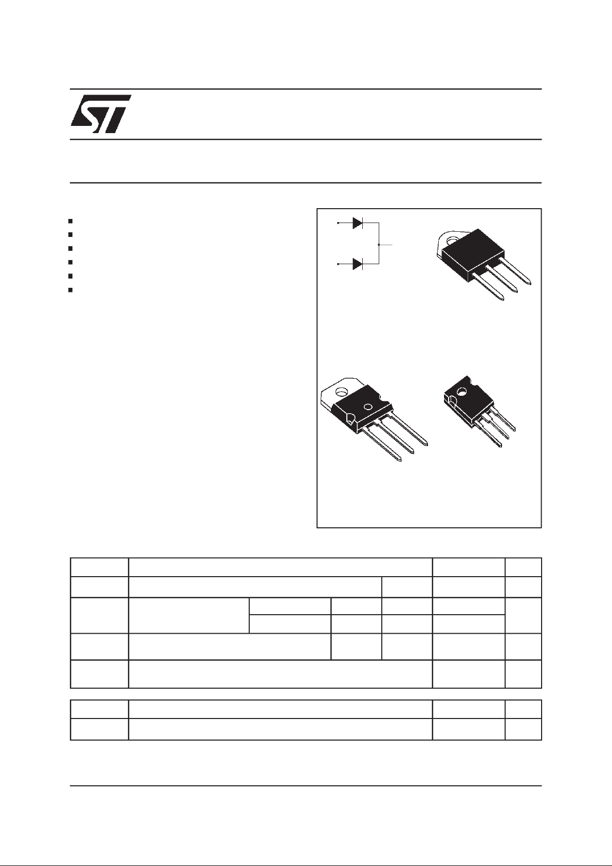
INSULATEDVERSIONTOP3I:
Insulatingvoltage= 2500 VDC
Capacitance= 12 pF
DESCRIPTION
Dual center tap rectifier suited for switchmode
power supply and high frequency DC to DC
converters.
Packagedin SOT93,TOP3I or TO247 this device
is intendedfor use in low voltage, high frequency
inverters, free wheeling and polarity protection
applications.
A1
A2
(Plastic)
BYW99P-200
SOT93
K
isolated
TOP3I
(Plastic)
BYW99PI-200
A2
K
A1
TO247
(Plastic)
BYW99W-200
ABSOLUTE MAXIMUMRATINGS
Symbol Parameter Value Unit
I
F(RMS)
I
F(AV)
I
FSM
Tstg
Tj
RMSforward current
Averageforwardcurrent
δ
=0.5
SOT93 / TO247 Tc=120°C Per diode
TOP3I Tc=115°C Per diode
Surgenon repetitiveforwardcurrent
Storageand junctiontemperaturerange
tp=10ms
sinusoidal
Per diode
Per diode
35 A
15 A
15
200 A
- 40 to + 150
- 40 to + 150
Symbol Parameter Value Unit
V
RRM
October 1999 Ed : 2A
Repetitivepeak reversevoltage
200 V
°
°C
C
1/6
Page 2

BYW99P/PI/W
THERMALRESISTANCES
Symbol Parameter Value Unit
Rth (j-c)
Rth (c)
Junctionto case
Coupling
SOT93 / TO247 Perdiode
Total
TOP3I Per diode
Total
SOT93 / TO247
TOP3I
1.8
1.0
2.0
1.25
0.2
0.5
Whenthe diodes1 and 2 are used simultaneously:
Tj-Tc(diode 1) = P(diode1) x R
STATICELECTRICAL CHARACTERISTICS
(Per diode)+ P(diode2) x R
th(j-c)
(Perdiode)
th(c)
Symbol TestConditions Min. Typ. Max. Unit
I
*
R
V
F**
=25°CV
T
j
T
= 100°C
j
Tj= 125°CI
=V
R
RRM
=12A
F
20
1.5 mA
0.85 V
°
C/W
°
C/W
µ
A
T
= 125°CI
j
T
=25°CI
j
Pulse test : * tp = 5 ms,δ <2%
** tp = 380µs,
<2%
δ
=25A
F
=25A
F
1.05
1.15
To evaluatethe conduction losses use the followingequation :
P = 0.65x I
F(AV)
+0.016 x I
F2(RMS)
RECOVERY CHARACTERISTICS
Symbol TestConditions Min. Typ. Max. Unit
trr T
tfr T
V
FP
=25°CI
j
=25°CI
j
Tj=25°CI
=0.5A
F
I
=1A
R
=1A
I
F
V
=30V
R
=1A
F
V
=1.1 x V
FR
=1A tr = 10 ns 2 V
F
Irr = 0.25A 25 ns
/dt = -50A/µs40
dI
F
tr=10ns 15 ns
F
2/6
Page 3

BYW99P/PI/W
Fig.1 : Average forward power dissipation versus
averageforward current.
P
F(av)(W)
20
17.5
=0.05
=0.1
=0.2 =0.5
=1
15
12.5
10
7.5
T
5
2.5
0
0 2.5 5 7.5 10 12.5 15 17.5 20
I
F(av)(A)
=tp/T
tp
Fig.3 : Forward voltage drop versus forward
current(maximumvalues).
VFM(V)
1.8
1.6
1.4
1.2
1.0
0.8
0.6
0.4
0.2
0.0
0.1 1 10 100 200
Tj=125 C
o
IFM(A)
Fig.2: Peakcurrent versusform factor.
I
M(A)
350
=tp/T
T
I
M
tp
300
250
200
150
100
50
P=10W
P=20W
P=30W
0
0 0.1 0.2 0.3 0.4 0.5 0.6 0.7 0.8 0.9 1
Fig.4 : Relative variation of thermal impedance
junctionto case versuspulse duration.
K
1.0
Zth(j-c) (tp. )
K=
Rth(j-c)
0.5
0.2
0.1
=0.5
=0.2
=0.1
T
Single puls e
tp(s)
1.0E-03 1.0E-02 1.0E-01 1. 0E+00
=tp/T
tp
Fig.5 :
Non repetitive surge peak forward current
versusoverloadduration.
(SOT93,TO247)
I
M(A)
160
150
140
130
120
110
100
90
80
70
60
50
IM
40
30
20
10
0
0.001 0.01 0.1 1
t
=0.5
t(s)
Tc=25 C
Tc=75 C
Tc=120 C
Fig.6 :
Non repetitive surge peak forward current
versusoverloadduration.
(TOP3I)
I
M(A)
160
150
140
130
120
110
100
o
o
o
90
80
70
60
50
IM
40
30
20
10
0
0.001 0.01 0.1 1
t
=0.5
t(s)
o
Tc=25 C
o
Tc=60 C
o
Tc=115 C
3/6
Page 4

BYW99P/PI/W
Fig.7 :
Average current versus ambient
temperature.
(δ= 0.5)(SOT93, TO247)
I
F(av)(A)
16
15
14
13
12
11
10
9
8
7
=0.5
6
5
4
3
2
=tp/T
1
0
0 20 40 60 80 100 120 140 160
Fig.9 :
Rth(j-a)=15 C/W
T
tp
Junction capacitance versus reverse
Rth(j-a)=Rth(j-c)
o
o
Tamb( C)
voltageapplied (Typical values).
C(pF)
200
190
180
170
160
150
140
130
120
110
100
1 10 100
F=1Mhz Tj=25 C
VR(V)
o
200
Fig.8 :
Average current versus ambient
temperature.
(δ= 0.5)(TOP3I)
I
F(av)(A)
16
15
14
13
12
11
10
9
8
7
=0.5
6
5
4
3
2
=tp/T
1
0
0 20 40 60 80 100 120 140 160
Fig.10 :
QRR(nC)
60
55
90%CONFIDENCE
50
IF=IF(av)
Rth(j-a)=15 C/W
T
tp
Recoverycharges versus dI
45
40
35
30
25
20
15
10
5
0
1 10 100
Rth(j-a)=Rth(j-c)
o
o
Tamb( C)
Tj=100 C
dIF/dt(A/us)
/dt.
F
O
O
Tj=25 C
Fig.11:
3.0
2.5
Peakreversecurrent versus dIF/dt.
IRM(A)
90%CONFIDENCE
IF=IF(av)
Tj=100 C
O
2.0
1.5
1.0
O
0.5
Tj=25 C
dIF/dt(A/us)
0.0
4/6
20
1 10 100
Fig.12 :
Dynamic parameters versus junction
temperature.
QRR;IRM[Tj]/QRR;IRM[Tj=125 C]
1.50
1.25
1.00
IRM
0.75
0.50
0.25
0.00
0 255075100125150
o
Tj( C)
o
QRR
Page 5

PACKAGEMECHANICAL DATA
SOT93
Marking: Type number
Coolingmethod : C
Weight: 5.3g
Recommendedtorque value : 0.8m.N
Maximumtorquevalue : 1.0m.N
PACKAGEMECHANICAL DATA
TOP3I (isolated)
BYW99P/PI/W
DIMENSIONS
REF.
A 4.70 4.90 1.185 0.193
C 1.90 2.10 0.075 0.083
D 2.50typ. 0.098typ.
D1 2.00typ. 0.078typ
E 0.50 0.78 0.020 0.031
F 1.10 1.30 0.043 0.051
F3 1.75typ 0.069typ
F4 2.10 typ. 0.083typ.
G 10.80 11.10 0.425 0.437
H 14.70 15.20 0.279 0.598
L 12.20 0.480
L2 16.20 0.638
L3 18.0 typ. 0.709typ.
L5 3.95 4.15 0.156 0.163
L6 31.00typ. 1.220typ.
O 4.00 4.10 0.157 0.161
Millimeters Inches
Min. Max. Min. Max.
Marking: Type number
Coolingmethod : C
Weight: 4.7g
Recommendedtorque value : 0.8m.N
Maximumtorquevalue : 1.0m.N
DIMENSIONS
REF.
Millimeters Inches
Min. Max. Min. Max.
A 4.4 4.6 0.173 0.181
B 1.45 1.55 0.057 0.061
C 14.35 15.60 0.565 0.614
D 0.5 0.7 0.020 0.028
E 2.7 2.9 0.106 0.114
F 15.8 16.5 0.622 0.650
G 20.4 21.1 0.815 0.831
H 15.1 15.5 0.594 0.610
J 5.4 5.65 0.213 0.222
K 3.4 3.65 0.134 0.144
L 4.08 4.17 0.161 0.164
P 1.20 1.40 0.047 0.055
R 4.60 typ. 0.181typ
5/6
Page 6

BYW99P/PI/W
PACKAGEMECHANICAL DATA
TO247
V
REF.
Millimeters Inches
DIMENSIONS
Min. Typ. Max. Min. Typ. Max.
V
Dia.
A 4.85 5.15 0.191 0.203
D 2.20 2.60 0.086 0.102
E 0.40 0.80 0.015 0.031
F 1.00 1.40 0.039 0.055
F1 3.00 0.118
H
A
F2 2.00 0.078
F3 2.00 2.40 0.078 0.094
L5
F4 3.00 3.40 0.118 0.133
G 10.90 0.429
L
L4L2
H 15.45 15.75 0.608 0.620
L 19.85 20.15 0.781 0.793
L1 3.70 4.30 0.145 0.169
L2 18.50 0.728
F1
V2
F4
F3
F2
L1
L3
D
L3 14.20 14.80 0.559 0.582
L4 34.60 1.362
L5 5.50 0.216
M 2.00 3.00 0.078 0.118
V5° 5°
F(x3)
G
==
ME
V2 60° 60°
Dia. 3.55 3.65 0.139 0.143
Marking
: Typenumber
Coolingmethod : C
Weight: 4.4g
Recommendedtorque value : 0.8m.N
Maximumtorquevalue : 1.0m.N
Informationfurnished is believed to be accurateand reliable. However, STMicroelectronics assumes no responsibility for theconsequences of
use of such informationnor forany infringementof patents or other rights of thirdparties which may result from its use.No license is grantedby
implication or otherwise under any patent or patent rights of STMicroelectronics. Specifications mentioned in this publication are subject to
change withoutnotice. This publication supersedes and replaces all informationpreviously supplied.
STMicroelectronics products are not authorized for use as critical components in life support devices or systems without express written approval of STMicroelectronics.
The ST logo is a registeredtrademark ofSTMicroelectronics
1999 STMicroelectronics - Printed in Italy - All rights reserved.
STMicroelectronics GROUP OF COMPANIES
Australia - Brazil - China - Finland - France - Germany - Hong Kong - India - Italy - Japan - Malaysia
Malta - Morocco - Singapore - Spain - Sweden - Switzerland - United Kingdom - U.S.A.
http://www.st.com
6/6
 Loading...