

Page 1
®
BYW98-200
HIGH EFFICI EN CY FAST RECO VE RY REC T IFIER DIODES
MAIN PRODUCT CHARACTERISTICS
I
F(AV)
V
RRM
3A
200 V
Tj (max) 150 °C
(max) 0.85 V
V
F
trr (max) 35 ns
FEATURES AND BE NE F ITS
VERY LOW CONDUCTION LOS SES
NEGLIGIBLE SWIT CHING LOS SE S
LOW FORWARD AND REVERSE RECOVERY
TIMES
DESCRIPTION
Low voltage drop and rectifier suited for switching
mode base drive and transistor circuits.
ABSOLUTE RATINGS
(limiting values)
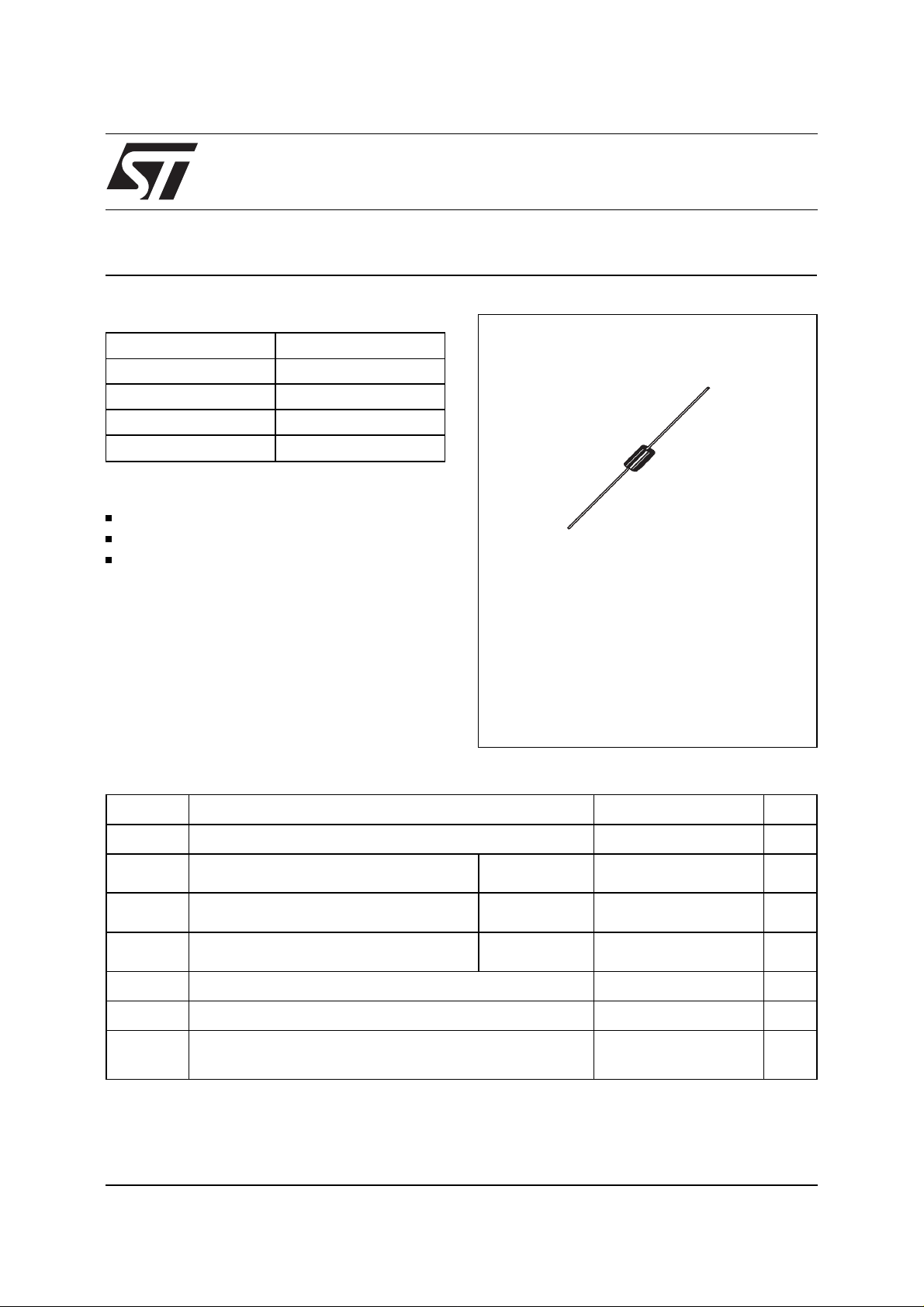
DO-201AD
(Plastic)
Symbol Parameter Value Unit
V
I
RRM
FRM
Repetitive peak reverse voltage
Repetitive peak forward current *
tp=5 µs
200 V
110 A
F=1KHz
I
F (AV)
I
FSM
Average forward current*
Surge non repetitive forward current
Ta = 75°C
δ
= 0.5
= 10ms
t
p
3A
70 A
Sinusoidal
T
stg
Tj
T
L
Storage temperature range
Maximum operating junction temperature
Maximum lead temperature for soldering during 10s at
- 65 to + 150
150
230
4mm from cas e
* On infinite heatsink with 10mm lead length.
October 1999 - Ed: 4C
°
C
°
C
°
C
1/5
Page 2
BYW98-200
THERMAL RE SISTA NC E
Symbol Parameter Value Unit
Rth (j-a)
* On infinite heatsink with 10mm lead length.
Junction-ambient *
25
STATIC ELECTRICAL CHARACTERISTICS
Symbol Parameter Test Conditions Min. Typ. Max. Unit
I
*
R
Reverse leakage
T
= 25°CV
j
current
= 100°C
T
j
V
**
F
Pulse test : * tp = 5 ms, δ < 2 %
To evaluate the conduction losses use the following equations:
P = 0.75 x I
Forward voltage drop T
** tp = 380 µs, δ < 2 %
+ 0.04 I
F(AV)
F2(RMS)
= 25°CI
j
= 100°CI
T
j
= V
R
= 9A
F
= 3A
F
RRM
10
0.5 mA
1.2 V
0.78 0.85
RECOVERY CHARACTE RISTIC S
°
C/W
µ
A
Symbol Test Conditions Min. Typ. Max. Unit
t
rr
Q
rr
t
fr
V
FP
Tj = 25°CI
V
= 30V
R
Tj = 25°CI
V
≤ 30V
R
Tj = 25°CI
= 1A dIF/dt = - 50A/µs
F
= 3A dIF/dt = - 20A/µs
F
= 3A dIF/dt = - 50A/µs
F
Measured at 1.1 x V
Tj = 25°CI
= 3A dIF/dt = - 50A/µs
F
max
F
35 ns
15 nC
20 ns
5V
2/5
Page 3

BYW98-200
Fig. 1:
Average forward power dissipation versus
average forward current.
PF(av)(W)
3.5
3.0
δ = 0.05
δ = 0.1
δ = 0.2
2.5
2.0
1.5
1.0
0.5
0.0
0.0 0.5 1.0 1.5 2.0 2.5 3.0 3.5
Fig. 3:
90
Thermal resistance versus lead length.
Rth(°C/W)
80
IF(av) (A)
Rth(j-a)
δ
70
60
50
40
30
Rth(j-l)
20
10
0
5 10152025
Lleads(mm)
δ = 0.5
=tp/T
δ = 1
T
tp
Fig. 2:
Average forward current versus ambient
temperature (δ=0.5).
IF(av)(A)
3.5
3.0
Rth(j-a)=Rth(j-l)
2.5
2.0
Rth(j-a)=75°C/W
1.5
1.0
0.5
0.0
0 25 50 75 100 125 150
Fig. 4:
T
δ
=tp/T
tp
Tamb(°C)
Variation of thermal impedance junction t o
ambient versus pulse duration (recommended pad
layout, epoxy FR4, e(Cu)=35µm).
Zth(j-a)/Rth(j-a)
1.00
δ = 0.5
δ = 0.2
δ = 0.1
0.10
T
Single pulse
0.01
tp(s)
1E-1 1E+0 1E+1 1E+2 5E+2
δ
=tp/T
tp
Fig. 5:
Forward voltage drop versus forward
current (maximum values).
IFM(A)
70.00
Tj=100°C
(Typical values)
10.00
Tj=25°C
1.00
0.10
0.0 0.2 0.4 0.6 0.8 1.0 1.2 1.4 1.6 1.8 2.0 2.2
Tj=100°C
VFM(V)
Fig. 6:
Junction capacitance versus reverse
voltage applied (typical values).
C(pF)
100
50
20
10
1 10 100 200
VR(V)
F=1MHz
Tj=25°C
3/5
Page 4

BYW98-200
Fig. 7:
Reverse recovery time versus dI
trr(ns)
100
80
Tj=100°C
/dt.
F
IF=3A
90% confidence
Tj=100°C
60
40
Tj=25°C
20
dIF/dt(A/µs)
0
1 10 100
Fig. 9:
Dynamic parameters versus junction
temperature.
%
250
200
IF=3A
dIF/dt=50A/µs
VR=30V
Qrr
Fig. 8:
dI
2.5
2.0
1.5
Peak reverse recovery current versus
/dt.
F
IRM(A)
IF=3A
90% confidence
Tj=100°C
Tj=100°C
1.0
0.5
Tj=25°C
0.0
1 10 100
dIF/dt(A/µs)
IRM
150
100
25 50 75 100 125 150
Tj(°C)
trr
4/5
Page 5

PACKAGE MECHANICAL DATA
DO-201AD
BYW98-200
BA
note 1
ØD ØD
DIMENSIONS
REF.
Millimeters Inches
Min. Max. Min. Max.
A 9.50 0.374
B 25.40 1.000
∅ C 5.30 0.209
∅ D 1.30 0.051
E 1.25 0.049
E
note 2
B
note 1
E
ØC
NOTES
1 - The lead diameter ∅ D is not controlled over zone E
2 - The minimum axial length within which the device may be
placed with its leads bent at right angles is 0.59"(15 mm)
Ordering code Marking Package Weight Base qty Delivery mode
BYW98-200 BYW98-200 DO-201AD 1.16 g. 600 Box
BYW98-200RL BYW98-200 DO-201AD 1.16 g. 1900 Tape and reel
White band indicates cathode
Epoxy meets UL94,V0
Information furnished is believed to be accurate and reliable. However, STMicroelectronics assumes no responsibility for the consequences of
use of such information nor for any infringement of patents or other rights of third parties which may result from its use. No license is granted by
implication or otherwi se un der any pat ent or patent rights of STMic roelec tronics. S pecifications ment ioned in t his publ ication are subject to
change without notice. This publication supersedes and replaces all information previously supplied.
STMicroelectronics products are not authorized for use as critical components in li fe s upport devices or systems wi thou t ex press written approval of STMicroelectronics.
The ST logo is a registered trademark of STMicroe lectronics
© 1999 STMicroelectronics - Printed in Italy - All rights reser ved.
STMicroelectronics GROUP OF COMPANIES
Australia - Brazil - China - Finland - France - Germany - Hong Kong - India - Italy - Japan - Malaysia
Malta - Morocco - Singapore - Spain - Sweden - Switzerland - United Kingdom - U.S.A.
http://www.st.com
5/5
 Loading...