

Page 1
1/6
BYW81G-200
BYW81P-200 / BYW81PI-200
®
July 2002 - Ed: 3E
HIGH EFFICIENCY FAST RECOVERY RECTIFIER DIODES
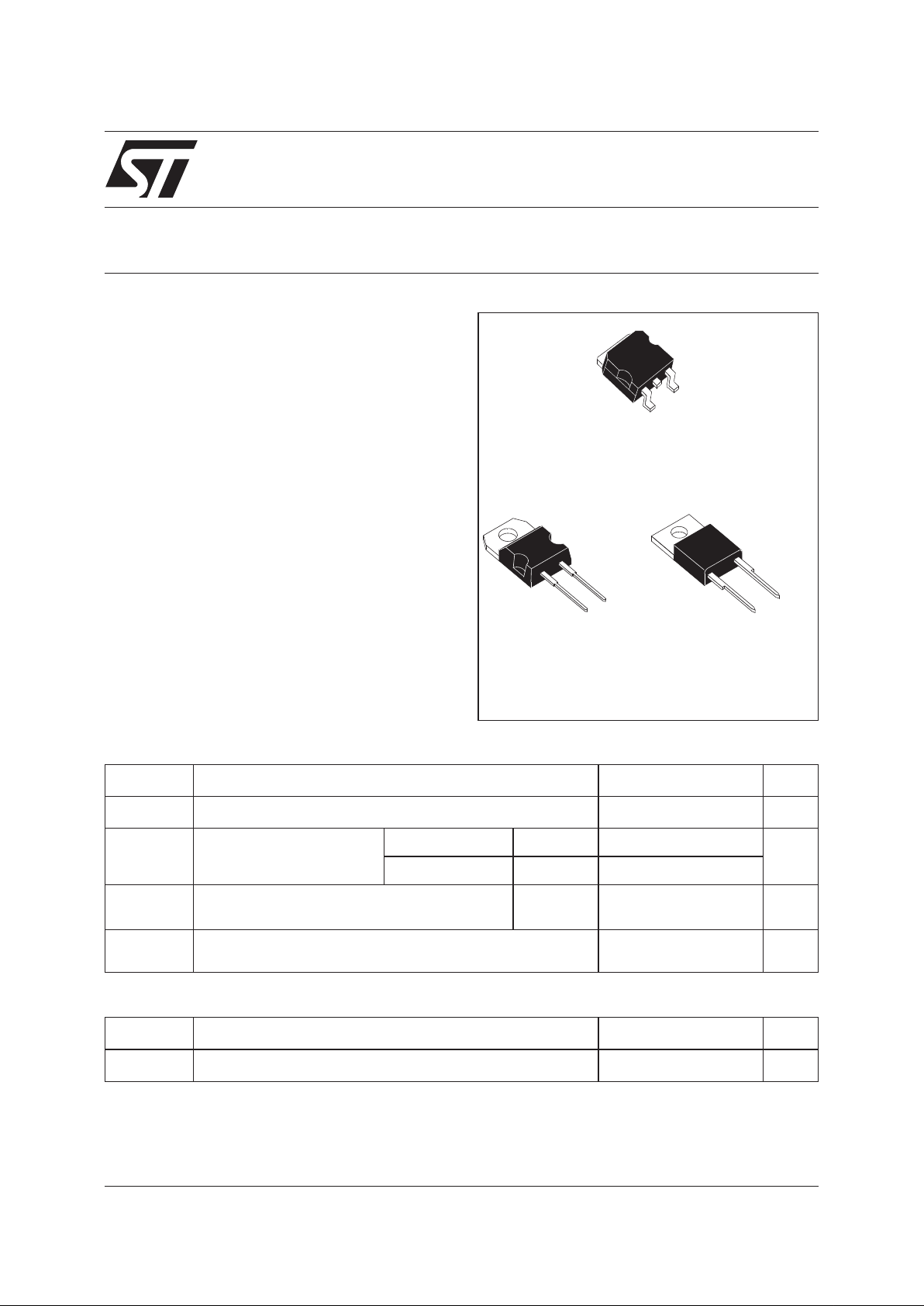
TO-220AC
(Plastic)
BYW81P-200
■
SUITED FOR SMPS
■
VERY LOW FORWARD LOSSES
■
NEGLIGIBLE SWITCHING LOSSES
■
HIGH SURGE CURRENT CAPABILITY
■
HIGH AVALANCHE ENERGY CAPABILITY
■
INSULATED VERSION :
Insulating voltage = 2500 V
RMS
Capacitance = 7 pF
DESCRIPTION
FEATURES
Single chip rectifier suited for switchmode power
supply and high frequency DC to DC converters.
Packaged in TO-220AC and D²PAK, this device is
intended for use in low voltage, high frequency
inverters, free wheeling and polarity protection
applications.
TO-220AC Ins.
(Plastic)
BYW81PI-200
Symbol Parameter Value Unit
I
F(RMS)
RMS forward current
35 A
I
F(AV)
Average forward current
δ = 0.5
BYW81P Tc=115°C
15 A
BYW81PI/G Tc=90°C
15
I
FSM
Surge non repetitive forward current
tp=10ms
sinusoidal
200 A
Tstg
Tj
Storage and junction temperature range
-40to+150
-40to+150
°C
°C
ABSOLUTE MAXIMUM RATINGS
Symbol Parameter Value Unit
V
RRM
Repetitive peak reverse voltage
200 V
K
A
K
A
K
NC
A
D2PAK
(Plastic)
BYW81G-200
Page 2

BYW81P-200 / BYW81PI-200 / BYW81G-200
2/6
Symbol Test Conditions Min. Typ. Max. Unit
I
R
*
T
j
= 25°C VR=V
RRM
20 µA
T
j
= 100°C
1.5 mA
V
F**
Tj= 125°C IF=12A
0.85 V
T
j
= 125°C IF=25A
1.05
T
j
= 25°C IF=25A
1.15
Pulse test :
* tp = 5 ms, duty cycle<2%
** tp = 380 µs, duty cycle<2%
ELECTRICAL CHARACTERISTICS
STATIC CHARACTERISTICS
Symbol Test Conditions Min. Typ. Max. Unit
trr T
j
= 25°C IF= 0.5A
IR=1A
Irr = 0.25A 25 ns
I
F
=1A
VR= 30V
dIF/dt = -50A/µs40
tfr T
j
= 25°C IF=1A
VFR=1.1xV
F
tr=10ns 15 ns
V
FP
Tj= 25°C IF=1A tr=10ns 2 V
RECOVERY CHARACTERISTICS
Symbol Parameter Value Unit
Rth (j-c)
Junction to case
BYW81P
2.0 °C/W
BYW81PI / G
3.5
THERMAL RESISTANCE
Page 3

BYW81P-200 / BYW81PI-200 / BYW81G-200
3/6
0.0 0.1 0.2 0.3 0.4 0.5 0.6 0.7 0.8 0.9 1.0
0
50
100
150
200
250
300
350
T
I
M
=tp/T
tp
I
M(A)
P=10W
P=20W
P=30W
Fig. 2: Peak current versus form factor.
0.1 1 10 100 200
Tj=125 C
o
IFM(A)
VFM(V)
0.0
0.2
0.4
0.6
0.8
1.0
1.2
1.4
1.6
1.8
Fig. 3: Forward voltage drop versus forward
current (maximum values).
0.1
1.0
0.2
0.5
Zth(j-c) (tp. )
K=
Rth(j-c)
=0.5
=0.2
=0.1
Single pulse
tp(s)
T
=tp/T
tp
1.0E-03 1.0E-02 1.0E-01
1.0E+00
K
Fig. 4: Relative variation of thermal impedance
junction to case versus pulse duration.
0 2.5 5 7.5 10 12.5 15 17.5 20
0.0
2.5
5.0
7.5
10.0
12.5
15.0
17.5
20.0
=0.05
=0.1
=0.2
=0.5
T
=tp/T
tp
I
F(av)(A)
P
F(av)(W)
=1
Fig. 1: Average forward power dissipation versus
average forward current.
0.001 0.01 0.1 1
0
10
20
30
40
50
60
70
80
90
100
110
120
IM
t
=0.5
t(s)
I
M(A)
Tc=25 C
o
Tc=60 C
o
Tc=90 C
o
Fig. 6: Non repetitive surge peak forward current
versus overload duration.
(BYW81PI / BYW81G)
0.001 0.01 0.1 1
0
10
20
30
40
50
60
70
80
90
100
110
120
130
140
150
160
IM
t
=0.5
t(s)
I
M(A)
Tc=25 C
o
Tc=75 C
o
Tc=115 C
o
Fig. 5: Non repetitive surge peak forward current
versus overload duration.
(BYW81P)
Page 4

BYW81P-200 / BYW81PI-200 / BYW81G-200
4/6
0 20 40 60 80 100 120 140 160
0
1
2
3
4
5
6
7
8
9
10
11
12
13
14
15
16
T
=tp/T
tp
=0.5
F(av)(A)
I
o
Tamb( C)
Rth(j-a)=15 C/W
o
Rth(j-a)=Rth(j-c)
Fig. 7: Average current versus ambient
temperature.
(duty cycle : 0.5) (BYW81P)
0 20 40 60 80 100 120 140 160
0
1
2
3
4
5
6
7
8
9
10
11
12
13
14
15
16
T
=tp/T
tp
=0.5
F(av)(A)
I
o
Tamb( C)
Rth(j-a)=15 C/W
o
Rth(j-a)=Rth(j-c)
Fig. 8: Average current versus ambient
temperature.
(duty cycle : 0.5) (BYW81PI / BYW81G)
1
80
85
10 30 50 70
90
95
100
105
110
115
120
VR(V)
F=1Mhz Tj=25 C
o
C(pF)
Fig. 9: Junction capacitance versus reverse
voltage applied (Typical values).
11020406080
0
10
20
30
40
50
60
QRR(nC)
90%CONFIDENCE
Tj=100 C
Tj=25 C
O
O
IF=IF(av)
dIF/dt(A/us)
Fig. 10: Recovery charges versus dIF/dt.
Tj( C)
QRR;IRM[Tj]/QRR;IRM[Tj=125 C]
0 25 50 75 100 125 150
0.00
0.25
0.50
0.75
1.00
1.25
1.50
IRM
QRR
o
o
Fig. 12: Dynamic parameters versus junction
temperature.
110
0.0
0.5
1.0
1.5
2.0
2.5
3.0
IRM(A)
dIF/dt(A/us)
20 40 60 80
90%CONFIDENCE
Tj=100 C
O
Tj=25 C
O
IF=IF(av)
Fig. 11: Peak reverse current versus dIF/dt.
Page 5

BYW81P-200 / BYW81PI-200 / BYW81G-200
5/6
■
Marking : Type number
■
Cooling method : C
■
Weight : 2.2 g
■
Recommended torque value : 0.8m.N
■
Maximum torque value : 1.0m.N
PACKAGE MECHANICAL DATA
TO-220AC (JEDEC outline)
■ Marking : Type number
■
Cooling method : C
■
Weight : 1.9 g
■
Recommended torque value : 0.8m.N
■ Maximum torque value : 1.0m.N
PACKAGE MECHANICAL DATA
TO-220AC (isolated)
A
C
D
E
M
L7
H2
Ø I
L5
L6
L9
L4
G
F1
F
L2
REF.
DIMENSIONS
Millimeters Inches
Min. Max. Min. Max.
A 4.40 4.60 0.173 0.181
C 1.23 1.32 0.048 0.051
D 2.40 2.72 0.094 0.107
E 0.49 0.70 0.019 0.027
F 0.61 0.88 0.024 0.034
F1 1.14 1.70 0.044 0.066
G 4.95 5.15 0.194 0.202
H2 10.00 10.40 0.393 0.409
L2 16.40 typ. 0.645 typ.
L4 13.00 14.00 0.511 0.551
L5 2.65 2.95 0.104 0.116
L6 15.25 15.75 0.600 0.620
L7 6.20 6.60 0.244 0.259
L9 3.50 3.93 0.137 0.154
M 2.6 typ. 0.102 typ.
Diam. I 3.75 3.85 0.147 0.151
b1
l2
a1
e
F
L
B
I
A
C
b2
c1
c2
a2
REF.
DIMENSIONS
Millimeters Inches
Min. Max. Min. Max.
A 14.23 15.87 0.560 0.625
a1 4.50 0.177
a2 12.70 14.70 0.500 0.579
B 10.20 10.45 0.402 0.411
b1 0.64 0.96 0.025 0.038
b2 1.15 1.39 0.045 0.055
C 4.48 4.82 0.176 0.190
c1 0.35 0.65 0.020 0.026
c2 2.10 2.70 0.083 0.106
e 4.58 5.58 0.180 0.220
F 5.85 6.85 0.230 0.270
I 3.55 4.00 0.140 0.157
L 2.54 3.00 0.100 0.118
l2 1.45 1.75 0.057 0.069
Page 6

BYW81P-200 / BYW81PI-200 / BYW81G-200
6/6
Informationfurnishedisbelievedtobeaccurateandreliable.However,STMicroelectronicsassumesnoresponsibilityfortheconsequencesof
useofsuchinformation nor for any infringement of patents or other rights of third parties which may result from its use. No license is granted by
implication or otherwise under any patent or patent rights of STMicroelectronics. Specifications mentioned in this publication are subject to
change without notice. This publication supersedes and replaces all information previously supplied.
STMicroelectronics products are not authorized for use as critical components in life support devices or systems without express written approval of STMicroelectronics.
The ST logo is a registered trademark of STMicroelectronics
© 2002 STMicroelectronics - Printed in Italy - All rights reserved.
STMicroelectronics GROUP OF COMPANIES
Australia - Brazil - Canada - China - Finland - France - Germany
Hong Kong - India - Israel - Italy - Japan - Malaysia - Malta - Morocco - Singapore
Spain - Sweden - Switzerland - United Kingdom - United States.
http://www.st.com
PACKAGE MECHANICAL DATA
D
2
PAK (Plastic)
A
C2
D
R
A2
M
V2
C
A1
G
L
L3
L2
B
B2
E
*
* FLAT ZONE NO LESSTHAN 2mm
REF.
DIMENSIONS
Millimeters Inches
Min. Max. Min. Max.
A 4.40 4.60 0.173 0.181
A1 2.49 2.69 0.098 0.106
A2 0.03 0.23 0.001 0.009
B 0.70 0.93 0.027 0.037
B2 1.14 1.70 0.045 0.067
C 0.45 0.60 0.017 0.024
C2 1.23 1.36 0.048 0.054
D 8.95 9.35 0.352 0.368
E 10.00 10.40 0.393 0.409
G 4.88 5.28 0.192 0.208
L 15.00 15.85 0.590 0.624
L2 1.27 1.40 0.050 0.055
L3 1.40 1.75 0.055 0.069
M 2.40 3.20 0.094 0.126
R 0.40 typ. 0.016 typ.
V2 0° 8° 0° 8°
8.90
3.70
1.30
5.08
16.90
10.30
FOOT PRINT DIMENSIONS (in millimeters)
D²PAK
■
Cooling method: by conduction (method C)
 Loading...