

Page 1
®
BYW80F/FP-200
HIGH EFFICIENCY FAST RECOVERY RECTIFIER DIODES
MAIN PRODUCTS CHARACTERISTICS
I
F(AV)
V
RRM
20 A
200 V
Tj (max) 150°C
(max) 0.85 V
V
F
trr (max) 35 ns
FEATURES
Suited for SMPS
■
Very low forward losses
■
Negligible switching losses
■
■ High surge current capability
■ Insulated packages:
ISOWATT220AC / TO-220FPAC:
Insulation voltage = 2000 V DC
Capacitance = 12 pF
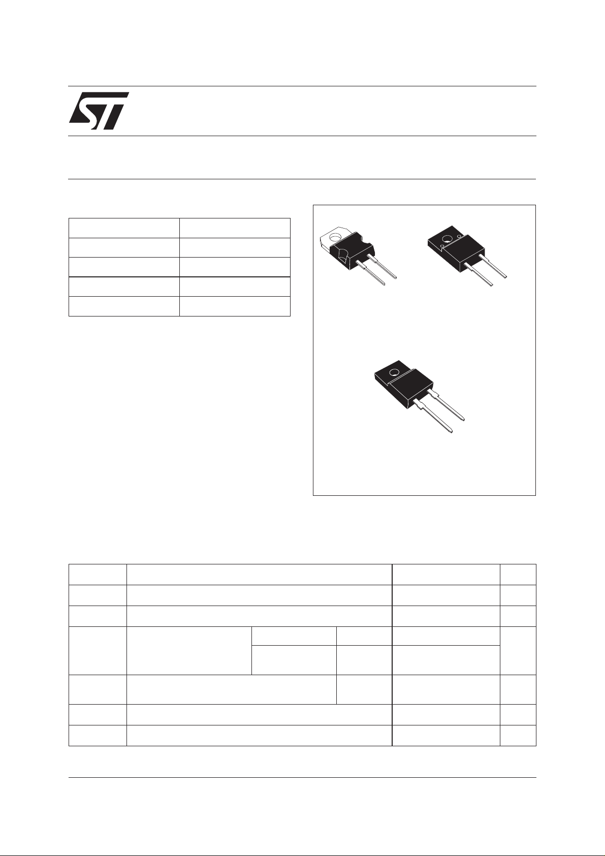
DESCRIPTION
Single chip rectifier suited for Switch Mode Power
SuppliesandhighfrequencyDC to DCconverters.
Packaged in TO-220AC, ISOWATT220AC and
TO-220FPAC this device is intended for use in low
voltage, high frequency inverters, free wheeling
and polarity protection applications.
K
TO-220AC
BYW80-200
A
ISOWATT220AC
BYW80F-200
TO-220FPAC
BYW80FP-200
A
K
A
K
ABSOLUTE MAXIMUM RATINGS
Symbol Parameter Value Unit
V
RRM
I
F(RMS)
I
F(AV)
Repetitive peak reverse voltage
RMS forward current
Average forward current
δ = 0.5
TO-220AC Tc=120°C
ISOWATT220AC
Tc=95°C
200 V
20 A
10 A
10
TO-220FPAC
I
FSM
Surge non repetitive forward current
tp=10ms
100 A
sinusoidal
Tstg
Tj
January 2002 - Ed: 3G
Storage and junction temperature range
Maximum operating temperature range
- 65 to + 150 °C
+ 150 °C
1/7
Page 2

BYW80F/FP-200
THERMAL RESISTANCE
Symbol Parameter Value Unit
Rth (j-c)
Junction to case
TO-220AC
ISOWATT220AC / TO-220FPAC
2.5 °C/W
4.7
ELECTRICAL CHARACTERISTICS
STATIC CHARACTERISTICS
Symbol Test Conditions Min. Typ. Max. Unit
*
I
R
V
F**
Pulse test:*tp=5ms,duty cycle<2%
= 25°C VR=V
T
j
= 100°C
T
j
Tj= 125°C IF=7A
T
= 125°C IF=15A
j
T
= 25°C IF=15A
j
** tp = 380 µs, duty cycle<2%
RRM
10 µA
1mA
0.85 V
1.05
1.15
To evaluate the conduction losses use the following equation :
P=0.65xI
F(AV)
+ 0.027 x I
F2(RMS)
RECOVERY CHARACTERISTICS
Symbol Test Conditions Min. Typ. Max. Unit
trr T
= 25°C IF= 0.5A
j
Irr = 0.25A 25 ns
IR=1A
I
=1A
F
dIF/dt = -50A/µs35
VR= 30V
tfr T
V
FP
=25°CI
j
=1A
F
VFR=1.1xV
tr=10ns 15 ns
F
Tj= 25°C IF=1A tr=10ns 2 V
2/7
Page 3
BYW80F/FP-200
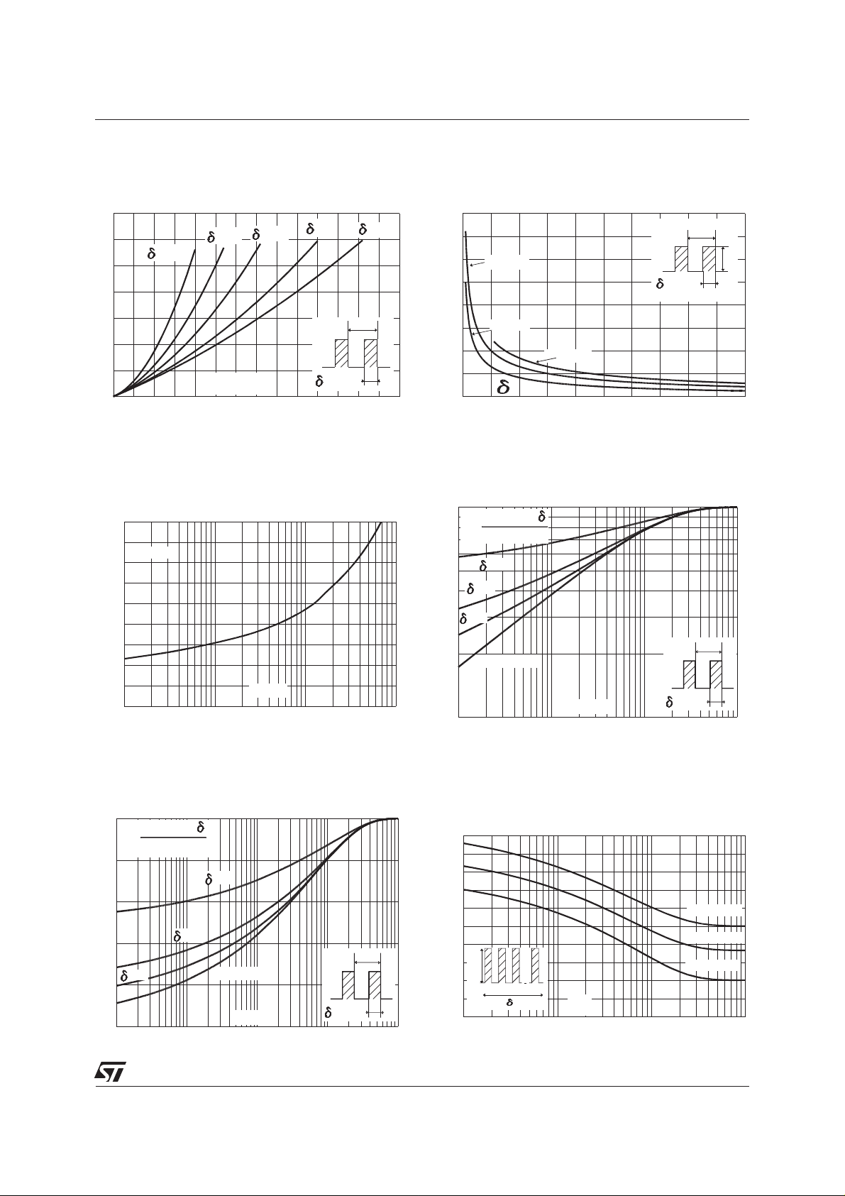
Fig. 1: Average forward power dissipation versus
average forward current
P
F(av)(W)
14
12
=0.05
=0.1
=0.2
=0.5
=1
10
8
6
T
4
2
0
01234567891011121314
I
F(av)(A)
=tp/T
tp
Fig. 3: Forward voltage drop versus forward current (maximum values)
VFM(V)
1.8
1.6
1.4
1.2
1.0
0.8
0.6
0.4
0.2
0.0
0.1 1 10 100
Tj=125 C
o
IFM(A)
Fig. 2: Peak current versus form factor
I
M(A)
200
=tp/T
T
I
M
tp
175
150
125
100
75
50
P=10W
P=5W
P=15W
25
0
0 0.1 0.2 0.3 0.4 0.5 0.6 0.7 0.8 0.9 1
Fig. 4: Relative variation of thermal impedance
junctionto case versuspulse duration (TO-220AC)
K
1.0
Zth(j-c) (tp. )
K=
Rth(j-c)
0.5
0.2
0.1
=0.5
=0.2
=0.1
Single pulse
tp(s)
1.0E-03 1.0E-02 1.0E-01
=tp/T
T
tp
1.0E+00
Fig. 5: Relative variation of thermal impedance
junction to case versus pulse duration.
(ISOWATT220AC / TO-220FPAC)
K
1
Zth(j-c) (tp. )
K=
Rth(j-c)
0.8
=0.5
0.6
0.4
=0.1
0.2
0
1.0E-03 1.0E-02 1.0E-01
=0.2
Single pulse
tp(s)
T
=tp/T
tp
1.0E+00 1.0E+01
Fig. 6: Non repetitive surge peak forward current
versus overload duration (TO-220AC)
I
M(A)
100
90
80
70
60
50
40
30
IM
20
10
0
0.001 0.01 0.1 1
t
=0.5
t(s)
o
Tc=25 C
Tc=75 C
o
Tc=120 C
o
3/7
Page 4

BYW80F/FP-200
Fig. 7: Non repetitive surge peak forward current
versus overload duration (ISOWATT220AC /
TO-220FPAC)
I
M(A)
80
70
60
50
o
40
30
IM
20
10
0
0.001 0.01 0.1 1 10
t
=0.5
t(s)
Tc=25 C
o
Tc=50 C
o
Tc=95 C
Fig. 9: Average current versus ambient temperature (duty cycle: 0.5) (ISOWATT220AC /
TO-220FPAC)
I
F(av)(A)
12
11
10
9
8
7
Rth(j-a)=15 C/W
o
6
=0.5
5
4
T
3
2
1
=tp/T
0
0 20 40 60 80 100 120 140 160
tp
Rth(j-a)=Rth(j-c)
o
Tamb( C)
Fig. 8: Average current versus ambient temperature (duty cycle : 0.5) (TO-220AC)
I
F(av)(A)
12
11
10
9
8
7
6
=0.5
5
4
3
2
=tp/T
1
0
0 20406080100120140160
Rth(j-a)=15 C/W
T
tp
Rth(j-a)=Rth(j-c)
o
o
Tamb( C)
Fig. 10: Junction capacitance versus reverse voltage applied (Typical values)
C(pF)
VR(V)
Fig. 11: Recovery charges versus dIF/dt.
QRR(nC)
90% CONFIDENCE Tj=125 C
4/7
o
dIF/dt(A/us)
IF=IF(av)
Fig. 12: Peak reverse current versus dIF/dt.
I
RM(A)
90% CONFIDENCE Tj=125 C
o
dIF/dt(A/us)
IF=IF(av)
Page 5

Fig. 13: Dynamic parameters versus junction
temperature
O
QRR;IRM[Tj]/QRR;IRM[Tj=125 C
IRM
Tj( C)
]
QRR
o
PACKAGE MECHANICAL DATA
TO-220AC (JEDEC outline)
BYW80F/FP-200
L2
DIMENSIONS
REF.
Millimeters Inches
Min. Max. Min. Max.
H2
Ø I
L5
A
C
L7
L6
A 4.40 4.60 0.173 0.181
C 1.23 1.32 0.048 0.051
D 2.40 2.72 0.094 0.107
E 0.49 0.70 0.019 0.027
F 0.61 0.88 0.024 0.034
F1 1.14 1.70 0.044 0.066
G 4.95 5.15 0.194 0.202
H2 10.00 10.40 0.393 0.409
L2 16.40 typ. 0.645 typ.
F1
L9
D
L4
L4 13.00 14.00 0.511 0.551
F
G
M
E
L5 2.65 2.95 0.104 0.116
L6 15.25 15.75 0.600 0.620
L7 6.20 6.60 0.244 0.259
L9 3.50 3.93 0.137 0.154
M 2.6 typ. 0.102 typ.
Diam. I 3.75 3.85 0.147 0.151
5/7
Page 6

BYW80F/FP-200
PACKAGE MECHANICAL DATA
ISOWATT220AC (JEDEC outline)
H
Diam
L6
L2
L3
F1
F
G
PACKAGE MECHANICAL DATA
TO-220FPAC
A
B
D E
DIMENSIONS
REF.
Millimeters Inches
Min. Max. Min. Max.
A 4.40 4.60 0.173 0.181
B 2.50 2.70 0.098 0.106
L7
D 2.40 2.75 0.094 0.108
E 0.40 0.70 0.016 0.028
F 0.75 1.00 0.030 0.039
F1 1.15 1.70 0.045 0.067
G 4.95 5.20 0.195 0.205
H 10.00 10.40 0.394 0.409
L2 16.00 typ. 0.63 typ.
L3 28.60 30.60 1.125 1.205
L6 15.90 16.40 0.626 0.646
L7 9.00 9.30 0.354 0.366
Diam 3.00 3.20 0.118 0.126
L3
L4
L2
G1
REF. DIMENSIONS
Millimeters Inches
A
H
B
A 4.4 4.6 0.173 0.181
Min. Max. Min. Max.
B 2.5 2.7 0.098 0.106
Dia
D 2.5 2.75 0.098 0.108
E 0.45 0.70 0.018 0.027
L6
L7
F 0.75 1 0.030 0.039
F1 1.15 1.70 0.045 0.067
G 4.95 5.20 0.195 0.205
L5
D
F1
G1 2.4 2.7 0.094 0.106
H 10 10.4 0.393 0.409
L2 16 Typ. 0.63 Typ.
L3 28.6 30.6 1.126 1.205
L4 9.8 10.6 0.386 0.417
F
E
L5 2.9 3.6 0.114 0.142
L6 15.9 16.4 0.626 0.646
G
L7 9.00 9.30 0.354 0.366
Dia. 3.00 3.20 0.118 0.126
6/7
Page 7

BYW80F/FP-200
Type Marking Package Weight Base Qty Delivery mode
BYW80-200
BYW80F-200
BYW80FP-200
Cooling method: by conduction (C)
■
Recommended torque value (ISOWATT220AC, TO-220FPAC): 0.55 nm
■
Maximum torque value (ISOWATT220AC, TO-220FPAC): 0.7 Nm
■
Recommended torque value (TO-220AC): 0.8 Nm
■
Maximum torque value (TO-220AC): 1.0 Nm
■
Epoxy meets UL94, V0
■
BYW80-200 TO-220AC 2.3 g 50 Tube
BYW80F-200 ISOWATT220AC 2 g 50 Tube
BYW80FP-200 TO-220FPAC 1.8 g 50 Tube
Informationfurnished is believed to be accurate andreliable.However, STMicroelectronics assumes no responsibility for theconsequences of
useof such information nor for anyinfringement of patents or other rightsof third parties which may resultfrom its use. No license isgranted by
implication or otherwise under any patent or patent rights of STMicroelectronics. Specifications mentioned in this publication are subject to
change without notice. This publication supersedes and replaces all information previously supplied.
STMicroelectronics products are not authorized for use as critical components in life support devices or systems without express written approval of STMicroelectronics.
The ST logo is a registered trademark of STMicroelectronics
© 2002 STMicroelectronics - Printed in Italy - All rights reserved.
STMicroelectronics GROUP OF COMPANIES
Australia - Brazil - Canada - China - Finland - France - Germany
Hong Kong - India - Israel - Italy - Japan - Malaysia - Malta - Morocco - Singapore
Spain - Sweden - Switzerland - United Kingdom - United States.
http://www.st.com
7/7
 Loading...