

Page 1
BYW77P/PI-200
HIGH EFFICIENCY FAST RECOVERY RECTIFIER DIODES
FEATURES
SUITEDFOR SMPS
VERYLOWFORWARD LOSSES
NEGLIGIBLESWITCHINGLOSSES
HIGHSURGE CURRENT CAPABILITY
HIGHAVALANCHEENERGYCAPABILITY
INSULATEDVERSION:
Insulatingvoltage= 2500 VDC
Capacitance= 12 pF
A
K
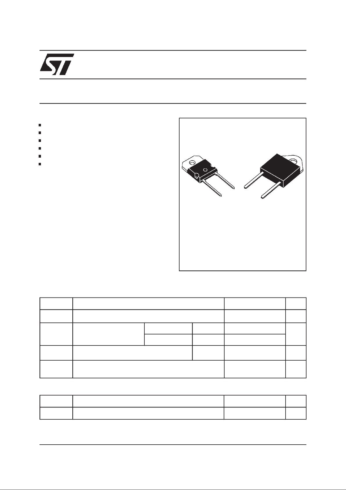
DESCRIPTION
Single chip rectifier suited for switchmode power
supplyand highfrequencyDC to DC converters.
Packaged in SOD93, or DOP3I this device is
intended for use in low voltage, high frequency
inverters, free wheeling and polarity protection
applications.
SOD93
(Plastic)
BYW77P-200
isolated
DOP3I
(Plastic)
BYW77PI-200
ABSOLUTE MAXIMUMRATINGS
Symbol Parameter Value Unit
I
F(RMS)
I
F(AV)
I
FSM
Tstg
Tj
RMSforward current 50 A
Averageforwardcurrent
δ = 0.5
Surgenon repetitiveforwardcurrent
SOD93 Tc=125°C
TOP3I Tc=100°C
tp=10ms
sinusoidal
25 A
25
500 A
Storageand junctiontemperaturerange - 40 to+ 150
- 40 to+ 150
Symbol Parameter Value Unit
V
RRM
October 1999 Ed : 2C
Repetitivepeak reversevoltage 200 V
°
°C
C
1/5
Page 2
BYW77P/PI-200
THERMALRESISTANCE
Symbol Parameter Value Unit
Rth(j-c) Junctionto case
SOD93
DOP3I
1.0 °C/W
1.8
ELECTRICAL CHARACTERISTICS
STATICCHARACTERISTICS
Symbol Test Conditions Min. Typ. Max. Unit
I
*T
R
V
F**
Pulse test : * tp = 5 ms, duty cycle < 2 %
=25°CV
j
T
= 100°C2.5mA
j
Tj= 125°CI
T
= 125°CI
j
T
=25°CI
j
** tp = 380µs, duty cycle < 2 %
=V
R
RRM
=20 A 0.85 V
F
=40 A 1.00
F
=40 A 1.15
F
25 µA
To evaluatethe conductionlossesusethefollowing equation:
P = 0.7x I
F(AV)
+ 0.0075x I
F2(RMS)
RECOVERYCHARACTERISTICS
Symbol Test Conditions Min. Typ. Max. Unit
trr T
tfr T
V
FP
2/5
=25°CI
j
=25°CI
j
Tj=25°CI
=0.5A
F
=1A
I
R
I
=1A
F
=30V
V
R
=1A
F
=1.1 x V
V
FR
=1A tr = 5 ns 1.5 V
F
Irr = 0.25A 35 ns
dI
/dt = -50A/µs50
F
tr = 5 ns 10 ns
F
Page 3

BYW77P/PI-200
Fig.1 : Average forward power dissipation versus
averageforward current.
P
F(av)(W)
30.0
27.5
25.0
=0.05
=0.1
=0.2
=0.5
=1
22.5
20.0
17.5
15.0
12.5
T
10.0
7.5
5.0
2.5
0.0
0 5 10 15 20 25 30
Fig.3 :
Forward voltage drop versus forward
I
F(av)(A)
=tp/T
tp
current(maximumvalues).
VFM(V)
1.8
1.6
1.4
1.2
1.0
0.8
0.6
0.4
0.2
0.0
0.1 1 10 100 300
Tj=125 C
o
IFM(A)
Fig.2: Peakcurrent versusform factor.
I
M(A)
500
T
400
P=20W
300
=tp/T
tp
200
P=30W
100
0
0 0.1 0.2 0.3 0.4 0.5 0.6 0.7 0.8 0.9 1
Fig.4 :
Relative variation of thermal impedance
P=40W
junctionto case versuspulse duration.
K
1.0
Zth(j-c) (tp. )
K=
Rth(j-c)
0.5
0.2
0.1
=0.5
=0.2
=0.1
T
Single pulse
tp(s)
1.0E-03 1.0E-02 1.0E-01 1.0E+00
=tp/T
I
M
tp
Fig.5 :
Non repetitive surge peak forward current
versusoverloadduration.
(BYW81P)
I
M(A)
300
250
200
150
100
IM
50
0
0.001 0.01 0.1 1
t
=0.5
t(s)
Tc=25 C
Tc=75 C
Tc=125 C
Fig.6 :
Non repetitive surge peak forward current
versusoverloadduration.
(BYW81PI)
I
M(A)
250
200
o
o
o
150
Tc=25 C
100
IM
50
0
0.001 0.01 0.1 1
t
=0.5
t(s)
Tc=50 C
Tc=100 C
o
o
o
3/5
Page 4

BYW77P/PI-200
Fig.7 :
Average current versus ambient
temperature.
(dutycycle : 0.5) (SOD93)
I
F(av)(A)
30
Rth(j-a)=Rth(j-c)
25
=0.5
20
T
15
10
Rth(j-a)=15 C/W
5
0
0 20 40 60 80 100 120 140 160
o
=tp/T
Tamb( C)
tp
o
Fig.9 : Junction capacitance versus reverse
voltageapplied(Typical values).
C(pF)
200
190
F=1Mhz Tj=25 C
180
170
160
150
140
130
120
110
100
110100
VR(V)
o
200
Fig.8 :
Average current versus ambient
temperature.
(dutycycle : 0.5) (DOP3I)
I
F(av)(A)
30
25
=0.5
20
Rth(j-a)=Rth(j-c)
T
15
10
Rth(j-a)=15 C/W
5
0
0 20 40 60 80 100 120 140 160
=tp/T
o
Tamb( C)
tp
o
Fig.10: Recoverychargesversus dIF/dt.
QRR(nC)
80
90%CONFIDENCE
70
IF=IF(av)
60
50
40
30
20
10
0
1 10 100
dIF/dt(A/us)
O
Tj=100 C
Tj=25 C
O
Fig.11:
Peakreversecurrent versus dIF/dt.
Fig.12 :
temperature.
IRM(A)
3.0
90%CONFIDENCE
IF=IF(av)
2.5
O
Tj=100 C
2.0
1.5
1.0
O
0.5
Tj=25 C
dIF/dt(A/ us)
0.0
4/5
20
110100
QRR;IRM[Tj]/QRR;IRM[Tj=125 C]
1.50
1.25
1.00
0.75
0.50
0.25
0.00
0 255075100125150
Dynamic parameters versus junction
o
IRM
QRR
o
Tj( C)
Page 5

PACKAGEMECHANICAL DATA
DOP3I(isoluted)
BYW77P/PI-200
DIMENSIONS
REF.
A 4.4 4.6 0.173 0.181
B 1.45 1.55 0.057 0.061
C 14.35 15.60 0.565 0.614
D 0.5 0.7 0.020 0.028
E 2.7 2.9 0.106 0.114
F 15.8 16.5 0.622 0.650
G 20.4 21.1 0.815 0.831
H 15.1 15.5 0.594 0.610
K 3.4 3.65 0.134 0.144
L 4.08 4.17 0.161 0.164
N 10.8 11.3 0.425 0.444
P 1.20 1.40 0.047 0.055
R 4.60 typ. 0.181typ.
Millimeters Inches
Min. Max. Min. Max.
Coolingmethod : C
Marking: Type number
Weight: 4.52 g
Recommendedtorque value: 0.8m.N
Maximumtorquevalue : 1.0m.N
5/5
Page 6

BYW77P/PI-200
PACKAGEMECHANICAL DATA
SOD93
DIMENSIONS
REF.
Millimeters Inches
Min. Typ. Max. Min. Typ. Max.
A 4.70 4.90 0.185 0.193
C 1.17 1.37 0.046 0.054
D 2.50 0.098
D1 1.27 0.050
E 0.50 0.78 0.020 0.031
F 1.10 1.30 0.043 0.051
F3 1.75 0.069
G 10.80 11.100.425 0.437
H 14.70 15.20 0.578 0.598
L 12.20 0.480
L2 16.20 0.638
L3 18.0 0.709
L5 3.95 4.15 0.156 0.163
L6 31.00 1.220
O 4.00 4.10 0.157 0.161
Coolingmethod : C
Marking: Type number
Weight: 3.79g
Recommendedtorque value: 0.8m.N
Maximumtorquevalue : 1.0m.N
Informationfurnished is believed to be accurate and reliable.However, STMicroelectronics assumes no responsibility for the consequences of
use of such informationnor for any infringementof patents or otherrights of third parties which may resultfrom its use.No license is granted by
implication or otherwise under any patent or patent rights of STMicroelectronics. Specifications mentioned in this publication are subject to
change without notice. This publication supersedes and replaces all information previously supplied.
STMicroelectronics products are not authorized for use as critical components in life support devices or systems withoutexpress written approval of STMicroelectronics.
The ST logo is a registeredtrademark ofSTMicroelectronics
1999 STMicroelectronics - Printed in Italy - All rights reserved.
STMicroelectronics GROUP OF COMPANIES
Australia - Brazil - China - Finland - France - Germany - Hong Kong - India - Italy- Japan - Malaysia
Malta - Morocco - Singapore - Spain - Sweden - Switzerland - United Kingdom - U.S.A.
http://www.st.com
6/5
 Loading...