

Page 1
HIGH EFFICIENCY FAST RECOVERY DIODES
MAINPRODUCTCHARACTERISTICS
BYW77G-200
I
F(AV)
V
RRM
25 A
200 V
trr 50 ns
V
F
0.85 V
FEATURESAND BENEFITS
VERYSMALLCONDUCTIONLOSSES
NEGLIGIBLESWITCHINGLOSSES
LOW FORWARD AND REVERSE RECOVERY
TIME
HIGHSURGECURRENTCAPABILITY
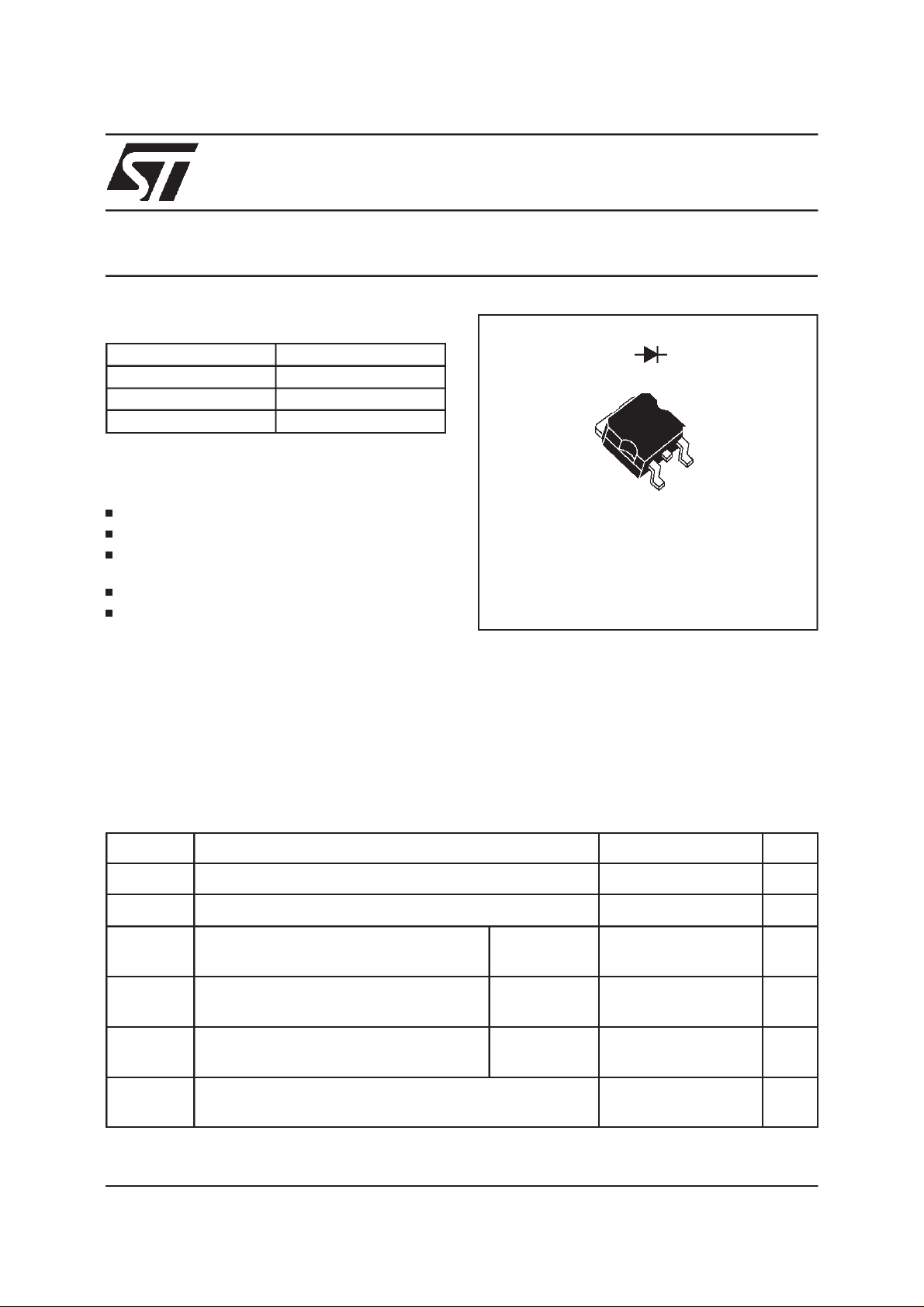
SMD PACKAGE
DESCRIPTION
Singlerectifiersuited for switchmodepowersupply
andhigh frequencyDC to DCconverters.
Packagedin D
2
PAK, this surface mount device is
intended for usein high frequencyinverters, free
wheelingand polarityprotectionapplications.
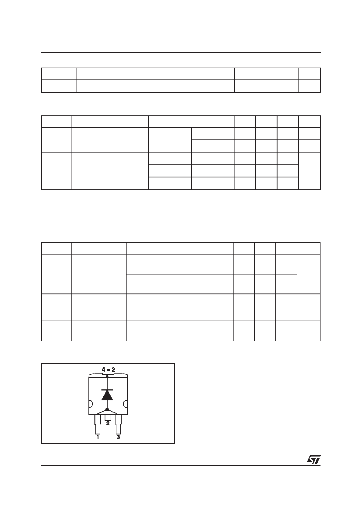
1&3 4
4
1
2
PAK
D
(Plastic)
2
3
ABSOLUTE MAXIMUM RATINGS
Symbol Parameter Value Unit
V
RRM
I
F(RMS)
I
F(AV)
Repetitivepeak reversevoltage 200 V
RMSforwardcurrent 50 A
Averageforward current Tc=125°C
25 A
δ = 0.5
I
FSM
Surgenon repetitiveforwardcurrent tp=10ms
200 A
sinusoidal
I
FRM
Repetitivepeak forwardcurrent tp = 5µs
310 A
f = 5 kHz
Tstg
Storageand junctiontemperaturerange - 40 to + 150
Tj
October 1999- Ed:3A
°
C
1/5
Page 2
BYW77G-200
THERMALRESISTANCE
Symbol Parameter Value Unit
R
th (j-c)
Junctionto case 1 °C/W
STATICELECTRICALCHARACTERISTICS
Symbol Parameter Test Conditions Min. Typ. Max. Unit
I
* Reverseleakage current VR=V
R
V
F**
Pulse test : * tp = 5 ms, δ <2%
Forwardvoltagedrop IF=20A Tj= 125°C 0.85 V
** tp = 380µs, δ<2%
RRM
I
=40A Tj= 125°C 1.00
F
I
=40A Tj=25°C 1.15
F
Tj=25°C25µA
= 100°C 2.5 mA
T
j
To evaluatethe conductionlossesuse thefollowingequation:
P = 0.65x I
F(AV)
+0.0075 I
F2(RMS)
RECOVERYCHARACTERISTICS
Symbol Parameter TestConditions Min. Typ. Max. Unit
t
rr
Reverserecovery
time
Tj=25°CI
Irr= 0.25A I
= 0.5A
F
=1A
R
35 ns
t
fr
Forwardrecovery
time
V
FP
Peakforward
voltage
PIN OUT configurationin D
=25°CI
T
j
dI
/dt= -50A/µsVR=30V
F
Tj=25°CI
/dt= 100A/µs
dI
F
V
= 1.1 x VFmax
FR
Tj=25°CIF=1A
dI
/dt= 100A/µs 1.5
F
2
PAK:
=1A
F
=1A
F
50
ns
10
V
2/5
Page 3

BYW77G-200
Fig.1 : Average forward power dissipation versus
averageforward current.
P
F(av)(W)
30.0
27.5
25.0
=0.05
=0.1
=0.2
=0.5
=1
22.5
20.0
17.5
15.0
12.5
T
10.0
7.5
5.0
2.5
0.0
0 5 10 15 20 25 30
I
F(av)(A)
=tp/T
tp
Fig.3 : Forward voltage drop versus forward cur-
rent(maximumvalues).
VFM(V)
1.8
1.6
1.4
1.2
1.0
0.8
0.6
0.4
0.2
0.0
0.1 1 10 100 300
Tj=125 C
o
IFM(A)
Fig.2: Peakcurrent versusform factor.
I
M(A)
500
T
400
P=20W
300
=tp/T
tp
200
P=30W
100
0
0 0.1 0.2 0.3 0.4 0.5 0.6 0.7 0.8 0.9 1
Fig.4 :
Relative variation of thermal impedance
P=40W
junctionto case versuspulse duration.
K
1.0
Zth(j-c) (tp. )
K=
Rth(j-c)
0.5
0.2
0.1
=0.5
=0.2
=0.1
T
Single pulse
tp(s)
1.0E-03 1.0E-02 1.0E-01 1.0E+00
=tp/T
I
M
tp
Fig.5 : Non repetitive surge peak forward current
versusoverload duration.
I
M(A)
300
250
200
o
150
100
IM
50
0
0.001 0.01 0.1 1
t
=0.5
t(s)
Tc=25 C
o
Tc=75 C
o
Tc=125 C
Fig.6 : Average current versus ambient tempera-
ture.(δ = 0.5)
I
F(av)(A)
30
25
=0.5
20
15
10
Rth(j-a)=15 C/W
5
0
0 20 40 60 80 100 120 140 160
o
=tp/T
o
Tamb( C)
Rth(j-a)=Rth(j-c)
T
tp
3/5
Page 4

BYW77G-200
Fig.7 :
Junction capacitance versus reverse volt-
Fig.8:
Reverserecoverychargesversus dI
age applied(Typical values).
C(pF)
200
190
F=1MHzTj=25 C
o
180
170
160
150
140
130
120
110
100
110100
Fig.9:
Peakreverse currentversus dIF/dt.
VR(V)
200
QRR(nC)
80
90%CONFIDENCE
70
IF=IF(av)
60
50
40
30
20
10
0
110100
Fig.10 :
perature.
IRM(A)
3.0
90%CONFIDENCE
IF=IF(av)
2.5
O
Tj=100 C
2.0
1.5
1.0
O
0.5
Tj=25 C
dIF/dt(A/µs)
0.0
20
110100
QRR;IRM[Tj]/QRR;IRM[Tj=125 C]
1.50
1.25
1.00
0.75
0.50
0.25
0.00
0 25 50 75 100 125 150
/dt.
F
O
Tj=100 C
O
Tj=25 C
dIF/dt(A/µs)
Dynamicparametersversus junction tem-
o
IRM
QRR
o
Tj( C)
4/5
Page 5

PACKAGEMECHANICALDATA
2
D
PAK(Plastic)
E
L2
L
L3
A1
B2
B
G
2.0 MIN.
FLAT ZONE
C2
BYW77G-200
DIMENSIONS
A
A 4.40 4.60 0.173 0.181
A1 2.49 2.69 0.098 0.106
A2 0.03 0.23 0.001 0.009
REF.
B 0.70 0.93 0.027 0.037
D
B2 1.14 1.70 0.045 0.067
C 0.45 0.60 0.017 0.024
C2 1.23 1.36 0.048 0.054
D 8.95 9.35 0.352 0.368
C
R
E 10.00 10.40 0.393 0.409
G 4.88 5.28 0.192 0.208
L 15.00 15.85 0.590 0.624
L2 1.27 1.40 0.050 0.055
A2
L3 1.40 1.75 0.055 0.069
M 2.40 3.20 0.094 0.126
R 0.40 typ. 0.016typ.
V2
V2 0° 8° 0° 8°
Millimeters Inches
Min. Max. Min. Max.
FOOT PRINT
10.30
Informationfurnished is believed to beaccurate and reliable. However, STMicroelectronics assumes no responsibility for the consequencesof
use of such information nor for any infringementof patents or other rights of third parties which may resultfrom its use. No license isgranted by
implication or otherwise under any patent or patent rights of STMicroelectronics. Specifications mentioned in this publication are subject to
change without notice. This publication supersedes and replaces all information previously supplied.
STMicroelectronics products are not authorized for use as critical components in life support devices or systems without express written approval of STMicroelectronics.
(inmillimeters)
16.90
5.08
1.30
3.70
8.90
The ST logo is a registered trademark ofSTMicroelectronics
1999 STMicroelectronics - Printed inItaly - All rights reserved.
STMicroelectronics GROUP OF COMPANIES
Australia - Brazil - China - Finland - France - Germany - Hong Kong - India- Italy - Japan - Malaysia
Malta - Morocco - Singapore - Spain - Sweden - Switzerland - United Kingdom - U.S.A.
http://www.st.com
5/5
 Loading...