

Page 1
HIGH EFFICIENCY FAST RECOVERY DIODES
MAINPRODUCTCHARACTERISTICS
BYW29G-200
I
F(AV)
V
RRM
8A
200 V
trr 35 ns
V
F
0.85V
FEATURESAND BENEFITS
VERYSMALL CONDUCTION LOSSES
NEGLIGIBLESWITCHING LOSSES
LOW FORWARD AND REVERSE RECOVERY
TIMES
HIGHSURGECURRENT
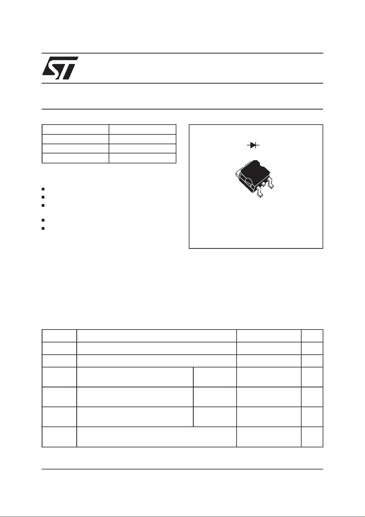
SMD
DESCRIPTION
Singlerectifiersuited forswitchmodepowersupply
and high frequencyDC to DCconverters.
PackagedinasurfacemountpackageD
2
PAK,this
device is intended for use in high frequency inverters,freewheelingandpolarityprotectionapplications.
AK
K
NC
2
PAK
D
(Plastic)
A
ABSOLUTE MAXIMUM RATINGS
Symbol Parameter Value Unit
V
RRM
I
F(RMS)
I
F(AV)
I
FSM
I
FRM
Repetitivepeak reversevoltage 200 V
RMSforwardcurrent 16 A
Averageforwardcurrent Tc=120°C
δ
=0.5
Surgenon repetitiveforwardcurrent
(Allpins connected)
tp=10ms
sinusoidal
Repetitivepeak forwardcurrent tp = 5 µs
8A
80 A
75 A
f = 5 kHz
Tstg
Storageand junctiontemperaturerange - 40 to+ 150 °C
Tj
October 1999 - Ed: 2
1/5
Page 2
BYW29G-200
THERMALRESISTANCE
Symbol Parameter Value Unit
Rth (j-c) Junctionto casethermal resistance 2.8
STATICELECTRICALCHARACTERISTICS
Symbol Parameter Test Conditions Min. Typ. Max. Unit
I
* Reverseleakagecurrent VR=V
R
V
F**
Pulse test : * tp = 5 ms, duty cycle < 2 %
Forwardvoltage drop IF=5A Tj= 125°C 0.85 V
** tp = 380 µs, dutycycle< 2 %
RRM
=10A Tj= 125°C 1.05
I
F
=10A Tj=25°C 1.15
I
F
Tj=25°C10
T
= 100°C 0.6 mA
j
To evaluatethe conductionlossesuse thefollowingequation:
P = 0.65x I
F(AV)
+0.040I
F2(RMS)
RECOVERYCHARACTERISTICS
Symbol Parameter TestConditions Min. Typ. Max. Unit
°
C/W
µ
A
t
rr
Reverserecovery
time
t
fr
Forwardrecovery
time
V
FP
Peakforward
voltage
PIN OUTconfigurationin D
Tj=25°CI
Irr = 0.25A I
T
=25°CI
j
/dt = -50A/µsV
dI
F
Tj=25°CI
/dt = 100A/µs
dI
F
= 1.1 x VFmax
V
FR
Tj=25°CIF=1A
/dt = 100A/µs2
dI
F
2
PAK:
= 0.5A
F
=1A
R
=1A
F
=
30V
R
=1A
F
25 ns
35
ns
15
V
2/5
Page 3

BYW29G-200
Fig.1 : Averageforward power dissipation versus
averageforward current.
P
F(av)(W)
12
=0.05 =0.1
=0.2
=0.5
=1
10
8
6
4
T
2
I
F(av)(A)
0
01234567891011
=tp/T
tp
Fig.3 : Forward voltage drop versus forward cur-
rent(maximumvalues).
VFM(V)
1.8
1.6
1.4
1.2
1.0
0.8
0.6
0.4
0.2
0.0
0.1 1 10 100
Tj=125 C
o
IFM(A)
Fig.2: Peakcurrent versusformfactor.
I
M(A)
160
140
T
120
100
80
60
40
P=10W
P=5W
P=15W
=tp/T
tp
20
0
0 0.1 0.2 0.3 0.4 0.5 0.6 0.7 0.8 0.9 1
Fig.4 :
Relative variation of thermal impedance
junctionto case versuspulse duration.
K
1.0
Zth(j-c) (tp. )
K=
Rth(j-c)
0.5
0.2
0.1
=0.5
=0.2
=0.1
T
Single pulse
tp(s)
1.0E-03 1.0E-02 1.0E-01 1. 0E+00
=tp/T
I
M
tp
Fig.5 : Non repetitive surge peak forward current
versusoverload duration.
I
M(A)
80
70
60
50
40
30
IM
20
10
0
0.001 0.01 0.1 1
t
=0.5
t(s)
o
Tc=25 C
o
Tc=75 C
o
Tc=120 C
Fig.6 : Average current versus ambient tempera-
ture.(duty cycle : 0.5)
I
F(av)(A)
10
9
8
7
6
5
=0.5
4
T
Rth(j-a)=15 C/W
3
2
1
=tp/T
0
0 20 40 60 80 100 120 140 160
tp
Rth(j-a)=Rth(j-c)
o
Tamb( C)
o
3/5
Page 4

BYW29G-200
Fig.7 :
Junction capacitance versus reverse volt-
age applied(Typical values).
C(pF)
VR(V)
Fig.9:
Peakreverse currentversus dIF/dt.
I
RM(A)
90% CONFIDENCE
O
Tj-100 C
F=1Mhz Tj=25 C
o
IF=IF(av)
Fig.8:
RecoverychargesversusdI
QRR(nC)
90%CONFIDENCE Tj-10 0 C
O
dIF/dt(A/us)
Fig.10 :
Dynamicparametersversus junctiontem-
perature.
QRR;IRM[Tj]/QRR;IRM[Tj=125 C]
o
/dt.
F
IF=IF(av)
dIF/dt(A/us)
IRM
o
Tj( C)
QRR
4/5
Page 5

PACKAGEMECHANICAL DATA
2
D
PAK(Plastic)
E
L2
L
L3
B2
B
G
* FLATZONE NO LESSTHAN2mm
C2
A1
M
BYW29G-200
DIMENSIONS
REF.
A
A 4.40 4.60 0.173 0.181
A1 2.49 2.69 0.098 0.106
A2 0.03 0.23 0.001 0.009
D
B 0.70 0.93 0.027 0.037
B2 1.14 1.70 0.045 0.067
C 0.45 0.60 0.017 0.024
C
R
C2 1.23 1.36 0.048 0.054
D 8.95 9.35 0.352 0.368
E 10.00 10.40 0.393 0.409
G 4.88 5.28 0.192 0.208
A2
L 15.00 15.85 0.590 0.624
L2 1.27 1.40 0.050 0.055
*
V2
L3 1.40 1.75 0.055 0.069
M 2.40 3.20 0.094 0.126
R 0.40typ. 0.016typ.
V2 0° 8° 0° 8°
Millimeters Inches
Min. Max. Min. Max.
FOOTPRINT
10.30
Informationfurnishedis believed to be accurate and reliable. However, STMicroelectronics assumes no responsibility for the consequences of
use of such information nor forany infringementof patents orother rights of thirdparties which may resultfromitsuse. Nolicense is grantedby
implication or otherwise under any patent or patent rights of STMicroelectronics. Specifications mentioned in this publication are subject to
change without notice.This publication supersedes andreplacesallinformationpreviously supplied.
STMicroelectronics products are not authorized for use as critical components in life support devices or systems withoutexpress written approval of STMicroelectronics.
(in millimeters)
16.90
5.08
1.30
3.70
8.90
The ST logo is a registered trademark of STMicroelectronics
1999STMicroelectronics - Printed in Italy - All rights reserved.
STMicroelectronics GROUP OF COMPANIES
Australia - Brazil - China - Finland- France - Germany - Hong Kong - India - Italy - Japan - Malaysia
Malta - Morocco - Singapore - Spain - Sweden - Switzerland - United Kingdom - U.S.A.
http://www.st.com
5/5
 Loading...