

Page 1
®
HIGH EFFIC IEN CY FAST REC OV ERY RECTIFIER DIO D E
MAIN PRODUCT CHARACTERISTI CS
BYW100-200
I
F(AV)
V
RRM
1.5 A
200 V
Tj (max) 150 °C
V
(max) 0.85 V
F
FEATURES AND BENE FITS
VERY LOW CO NDU CT ION LOSS E S
NEGLIGIBLE SWITCHING LOSSE S
LOW FORWARD AND REVERSE RECOVERY
TIMES
THE SPECIFICATIONS AND CURVES
ENABLE THE DETERMINATION OF trr AND
AT 100°C UNDER USE RS CO ND ITIONS
I
RM
DESCR IPT ION
Low voltage drop and rectifier s uited for switching
mode base drive and transistor circuits.
F126
(JEDEC DO-204AC)
ABSOLUTE RATINGS (limiting values)
Symbol Parameter Value Unit
V
RRM
I
FRM
I
F(AV)
I
FSM
T
T
Tj
stg
Repetitive peak reverse voltage
Repetitive peak forward current * tp = 5 µs F = 1K Hz
Average forward current * Ta = 95°C δ = 0.5
Surge non repetitive forward current tp=10 ms sinusoidal
Storage temperature range
Maximum operating junction temperature
L
Maximum lead temperature for soldering during 10s at 4mm from
200 V
80 A
1.5 A
50 A
-65 +150 °C
+ 150 °C
230 °C
case
* On infinite heatsink with 10mm lead length.
October 1999 - Ed: 3A
1/5
Page 2
BYW100-200
THERMA L RE SISTA NC ES
Symbol Parameter Value Unit
R
th (j-a)
* On infinite heatsink with 10mm lead length.
Junction to ambient *
STATIC ELECTRICAL CHARACTE RISTICS (per diode)
Symbol Parameter Tests conditions Min. Typ. Max. Unit
45 °C/W
*
I
R
Reverse leakage
current
V
**
F
Pulse test : * tp = 5 ms, δ < 2 %
Forward voltage drop I
** tp = 380 µs, δ < 2 %
V
R
= V
RRM
Tj = 25 °C
Tj = 100°C
= 4.5 A Tj = 25°C
F
IF = 1.5 A Tj = 100°C
0.78 0.85
10 µA
0.5 mA
1.2 V
To evaluate the maximum conduction losses use the following equation :
P = 0.75 x I
F(AV)
+ 0.075 I
F2(RMS )
RECOVERY CH ARACTE RIST ICS
Symbol Tests conditions Min. Typ. Max. Unit
trr
tfr
V
Qrr
FP
= 1 A dIF/dt = - 50 A/µs VR = 30 V Tj = 25°C
I
F
I
= 1.5 A dIF/dt = -50 A/µs
F
Measured at 1.1 x V
max.
F
Tj = 25 °C
IF = 1.5 A dIF/dt = -50 A/µs Tj = 25°C
I
= 1.5 A dIF/dt = -20 A/µs VR ≤ 30 V Tj = 25°C
F
30 ns
5V
10 nC
35 ns
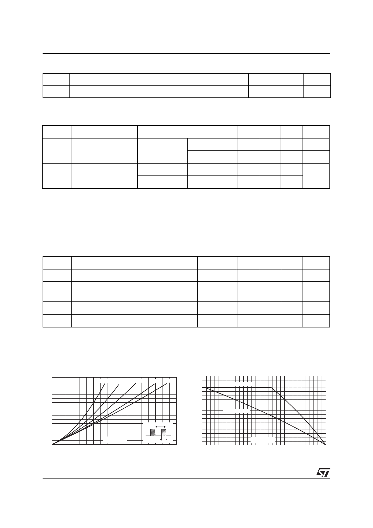
Fig. 1: Average forward power dissipation versus
average forward current.
PF(av)(W)
1.6
1.4
1.2
1.0
0.8
0.6
0.4
0.2
0.0
0.0 0.2 0.4 0.6 0.8 1.0 1.2 1.4 1.6 1.8
2/5
δ = 0.05
IF(av) (A)
δ = 0.1
δ = 0.2
δ
δ = 0.5
=tp/T
δ = 1
T
tp
Fig. 2: Average forward current versus ambient
temperature (δ=0.5).
IF(av)(A)
1.8
1.6
1.4
1.2
1.0
0.8
0.6
0.4
0.2
0.0
0 25 50 75 100 125 150
Rth(j-a)=Rth(j-l)
Rth(j-a)=100°C/W
Tamb(°C)
Page 3

BYW100-200
Fig. 3: Thermal resistance versus lead length.
Rth(°C/W)
110
100
Rth(j-a)
90
80
70
60
Rth(j-l)
50
40
30
20
10
0
5 10152025
Lleads(mm)
Fig. 5: Forward voltage drop versus forward
current (maximum values).
IFM(A)
50.00
Tj=100°C
(Typical values)
10.00
Tj=25°C
1.00
0.10
0.0 0.2 0.4 0.6 0.8 1.0 1.2 1.4 1.6 1.8 2.0 2.2 2.4 2.6
Tj=100°C
VFM(V)
Fig. 4: Variation of thermal impedance junction to
ambient versus pulse duration (recommended pad
layout, epoxy FR4, e( Cu)=35µ m).
Zth(j-a)/Rth(j-a)
1.00
δ = 0.5
δ = 0.2
0.10
δ = 0.1
Single pulse
0.01
1E-2 1E-1 1E+0 1E+1 1E+2 5E+2
tp(s)
Fig. 6: Junction capacitance versus reverse
voltage applied (typical values).
C(pF)
20
10
5
2
VR(V)
1
1 10 100 200
F=1MHz
Tj=25°C
Fig. 7: Reverse recovery time versus dI
trr(ns)
150
Tj=100°C
/dt .
F
IF=1.5A
VR=30V
90% confidence
100
Tj=25°C
50
0
1 10 100
dIF/dt(A/µs)
Fig. 8: Peak reverse recovery current versus
dI
/dt.
F
IRM(A)
2.5
2.0
1.5
1.0
0.5
0.0
IF=1.5A
VR=30V
90% confidence
Tj=100°C
Tj=25°C
dIF/dt(A/µs)
1 10 100
3/5
Page 4

BYW100-200
Fig. 9: Dynamic parameters versus junction
temperature.
%
250
200
Qrr
IRM
150
100
25 50 75 100 125
Tj(°C)
trr
4/5
Page 5

PACKAGE MECHANICAL DAT A
F126
BYW100-200
A
D
CC
D
B
DIMENSIONS
REF.
A
B
C
D
Ordering code Marking P ackage Weight Base qty Delivery mode
Millimeters Inches
Min. Typ. Max. Min. Typ. Max.
6.05 6.20 6.35 0.238 0.244 0.250
2.95 3.00 3.05 0.116 0.118 0.120
26 31 1.024 1.220
0.76 0.81 0.86 0.030 0.032 0.034
BYW100-200 BYW100-200 F126 0.393g 1000 Ammopack
BYW100-200RL BYW100-200 F126 0.393g 6000 Tape and reel
Cooling method: by conduction (method A)
Epoxy meets UL 94, V0
Information furnished is believed to be accurate and reliable. However, STMicroelectronics assumes no responsibility for the consequences of
use of such information nor for any infringement of patents or other rights of third parties which may result from its use. No license is granted by
implication or otherwi se un der any pat ent or patent rights of STMic roelec tronics. S pecifications ment ioned in t his publ ication are subject to
change without notice. This publication supersedes and replaces all information previously supplied.
STMicroelectronics products are not authorized for use as critical components in li fe s upport devices or systems wi thout express writte n approval of STMicroelectronics.
The ST logo is a registered trademark of STMicroe lectronics
© 1999 STMicroelectronics - Printed in Italy - All rights reser ved.
STMicroelectronics GROUP OF COMPANIES
Australia - Brazil - China - Finland - France - Germany - Hong Kong - India - Italy - Japan - Malaysia
Malta - Morocco - Singapore - Spain - Sweden - Switzerland - United Kingdom - U.S.A.
http://www.st.com
5/5
 Loading...