

Page 1
BYV54V
BYV541V
HIGH EFFICIENCY FAST RECOVERY RECTIFIER DIODES
FEATURES
n SUITED FOR SMPS
n VERY LOWFORWARD LOSSES
n NEGLIGIBLE SWITCHING LOSSES
n HIGH SURGE CURRENT CAPABILITY
n HIGH AVALANCHE ENERGY CAPABILITY
n INSULATED :
Insulating voltage = 2500 V
RMS
Capacitance = 45 pF
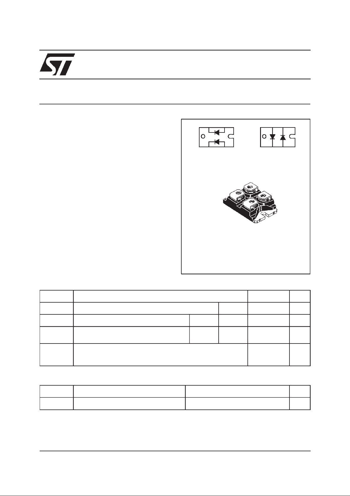
DESCRIPTION
Dual rectifier suited for switchmode power supply
and high frequency DC to DC converters.
Packaged in ISOTOPTMthis device is intended for
use in low voltage, high frequency inverters, free
wheeling and polarity protection applications.
K2 A2
A1K1
BYV541V-200
ISOTOP
(Plastic)
A2 K1
BYV54V-200
A1K2
ABSOLUTE MAXIMUM RATINGS
Symbol Parameter Value Unit
I
F(RMS)
I
F(AV)
I
FSM
RMS forward current
Average forward current δ = 0.5
Surge non repetitive forward current
Per diode
Tc=90°C Per diode
tp=10ms
Per diode
100 A
50 A
1000 A
sinusoidal
Tstg
Tj
Storage and junction temperature range
-40to+
150
- 40 to+ 150
Symbol Parameter BYV54V / BYV541V Unit
V
RRM
Repetitive peak reverse voltage
200 V
ISOTOP is a trademark of STMicroelectronics.
May 2000 - Ed : 2E
°C
°C
1/5
Page 2
BYV54V / BYV541V
THERMAL RESISTANCE
Symbol Parameter Value Unit
Rth (j-c)
Rth (c)
Junction to case
Coupling
Per diode
Total
1.2 °C/W
0.85
0.1 °C/W
When the diodes 1 and 2 are used simultaneously :
Tj-Tc (diode 1) = P(diode 1) x Rth(j-c)(Per diode) + P(diode 2) x Rth(c)
ELECTRICAL CHARACTERISTICS (Per diode)
STATIC CHARACTERISTICS
Symbol Test Conditions Min. Typ. Max. Unit
IR*
V
F**
Tj=25°CV
=V
R
RRM
Tj= 100°C
Tj= 125°CI
Tj= 125°CI
=50A
F
= 100 A
F
50 µA
5mA
0.85 V
1.00
Tj=25°CI
Pulse test :
* tp = 5 ms, duty cycle < 2%
** tp = 380 µs, duty cycle< 2 %
= 100 A
F
1.15
RECOVERY CHARACTERISTICS
Symbol Test Conditions Min. Typ. Max. Unit
trr Tj=25°CI
= 0.5A
F
Irr = 0.25A 40 ns
IR=1A
IF=1A
dIF/dt = -50A/µs60
VR= 30V
tfr Tj=25°CI
V
FP
Tj=25°CI
=1A
F
VFR= 1.1 x V
= 1A tr = 5ns 1.5 V
F
tr = 5ns 10 ns
F
2/5
Page 3

BYV54V / BYV541V
Fig.1 : Average forward power dissipation versus
average forward current.
P
F(av)(W)
45
40
35
=0.05
=0.1
=0.2
=0.5
=1
30
25
20
T
15
10
5
0
0 5 10 15 20 25 30 35 40 45 50
I
F(av)(A)
=tp/T
tp
Fig.3 : Forward voltage drop versus forward
current (maximum values).
VFM(V)
1.8
1.6
1.4
1.2
1.0
0.8
0.6
0.4
0.2
0.0
o
Tj=125 C
IFM(A)
110100500
Fig.2 : Peak current versus form factor.
I
M(A)
1000
=tp/T
T
I
M
tp
800
P=30W
600
400
200
0
P=15W
P=45W
P=60W
0.0 0.1 0.2 0.3 0.4 0.5 0.6 0.7 0.8 0.9 1.0
Fig.4 : Relative variation of thermal impedance
junction to case versus pulse duration.
K
1.0
Zth(j-c) (tp. )
K=
Rth(j-c)
0.5
0.2
0.1
=0.5
=0.2
=0.1
Single pulse
tp(s)
1.0E-03 1.0E-02 1.0E-01
=tp/T
T
tp
1.0E+00
Fig.5 : Non repetitive surge peak forward current
versus overload duration.
I
M(A)
400
300
o
200
100
IM
t
0
0.001 0.01 0.1 1
=0.5
t(s)
Tc=25 C
o
Tc=50 C
o
Tc=90 C
Fig.6 : Average current versus ambient
temperature. (duty cycle :0.5)
I
F(av)(A)
60
50
40
30
=0.5
20
T
10
=tp/T
0
0 20 40 60 80 100 120 140 160
tp
Rth(j-a)=Rth(j-c)
o
Tamb( C)
3/5
Page 4

BYV54V / BYV541V
Fig.7 : Junction capacitance versus reverse
voltage applied (Typical values).
C(pF)
420
400
380
360
340
320
300
280
260
240
1 10 100
F=1Mhz Tj=25 C
VR(V)
o
200
Fig.9 : Peak reverse current versus dIF/dt.
IRM(A)
4.0
90%CONFIDEN CE
3.6
IF=IF(av)
3.2
2.8
2.4
2.0
1.6
1.2
0.8
0.4
0.0
20
1 10 100
dIF/dt(A/us)
O
Tj=100 C
Tj=25 C
O
Fig.8 : Recovery charges versus dIF/dt.
QRR(nC)
120
90%CONFIDENCE
110
90
IF=IF(av)
O
Tj=100 C
100
80
70
60
O
50
Tj=25 C
40
30
20
10
0
110100
dIF/dt(A/us)
Fig.10 : Dynamic parameters versus junction
temperature.
QRR;IRM[Tj]/QRR;IRM[Tj=125 C]
1.50
1.25
1.00
IRM
0.75
0.50
0.25
0.00
0 25 50 75 100 125 150
o
Tj( C)
o
QRR
4/5
Page 5

PACKAGE MECHANICAL DATA
ISOTOP
BYV54V / BYV541V
DIMENSIONS
REF.
A 11.80 12.20 0.465 0.480
A1 8.90 9.10 0.350 0.358
B 7.8 8.20 0.307 0.323
C 0.75 0.85 0.030 0.033
C2 1.95 2.05 0.077 0.081
D 37.80 38.20 1.488 1.504
D1 31.50 31.70 1.240 1.248
E 25.15 25.50 0.990 1.004
E1 23.85 24.15 0.939 0.951
E2 24.80 typ. 0.976 typ.
G 14.90 15.10 0.587 0.594
G1 12.60 12.80 0.496 0.504
G2 3.50 4.30 0.138 0.169
F 4.10 4.30 0.161 0.169
F1 4.60 5.00 0.181 0.197
P 4.00 4.30 0.157 0.69
P1 4.00 4.40 0.157 0.173
S 30.10 30.30 1.185 1.193
Millimeters Inches
Min. Max. Min. Max.
n Marking : Type number
n Cooling method : C
n Weight : 27 g
n Epoxy meets UL94, V0
Informationfurnishedis believed to beaccurate andreliable. However,STMicroelectronicsassumes no responsibilityfor the consequencesof
useof such information nor for anyinfringement ofpatents orother rights of third parties which mayresultfrom its use. No licenseis grantedby
implication or otherwise under any patent or patent rights of STMicroelectronics. Specifications mentioned in this publication are subject to
change without notice. This publication supersedesand replacesall information previously supplied.
STMicroelectronics products are not authorized for use as critical components in life support devices or systems without express written approvalof STMicroelectronics.
The ST logo is a registered trademark of STMicroelectronics
2000 STMicroelectronics - Printed in Italy -All rights reserved.
STMicroelectronics GROUP OF COMPANIES
Australia - Brazil - China - Finland - France - Germany - Hong Kong - India - Italy - Japan - Malaysia
Malta - Morocco - Singapore - Spain - Sweden - Switzerland - United Kingdom - U.S.A.
http://www.st.com
5/5
 Loading...