

Page 1
BYV255V
HIGH EFFICIENCY FAST RECOVERY RECTIFIER DIODES
FEATURES
n SUITED FOR SMPS
n VERY LOW FORWARD LOSSES
n NEGLIGIBLE SWITCHINGLOSSES
n HIGH SURGECURRENT CAPABILITY
n HIGH AVALANCHEENERGY CAPABILITY
n INSULATED :
Insulating voltage =2500 V
RMS
Capacitance =55 pF
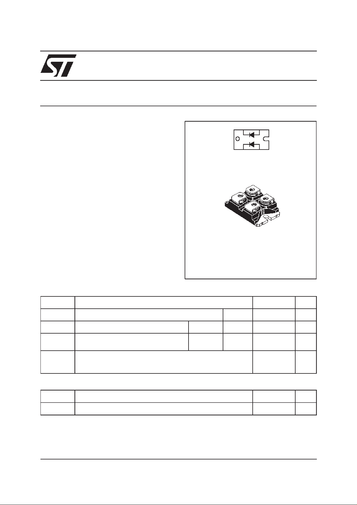
DESCRIPTION
Dual rectifier suited for switchmode power supply
and high frequency DCto DC converters.
Packaged in ISOTOPTMthis device is intended for
use in low voltage, high frequency inverters, free
wheeling and polarity protectionapplications.
ABSOLUTE MAXIMUM RATINGS
K2 A2
A1K1
ISOTOP
(Plastic)
Symbol Parameter Value Unit
I
F(RMS)
I
F(AV)
I
FSM
RMS forward current
Average forward current δ = 0.5
Surge non repetitive forward current
Per diode
Tc=110°C Per diode
tp=10ms
Per diode
150 A
100 A
1600 A
sinusoidal
Tstg
Tj
Storage and junction temperature range
-40to+
150
- 40 to + 150
Symbol Parameter Value Unit
V
RRM
Repetitive peak reverse voltage
200 V
ISOTOP is a trademark of STMicroelectronics.
May 2000 - Ed : 2E
°C
°C
1/5
Page 2
BYV255V
THERMAL RESISTANCE
Symbol Parameter Value Unit
Rth (j-c)
Rth (c)
Junction to case
Coupling
Per diode
Total
0.4 °C/W
0.25
0.1 °C/W
When the diodes 1 and 2 are used simultaneously :
Tj-Tc (diode 1) = P(diode1) x Rth(j-c)(Per diode) + P(diode 2) xRth(c)
ELECTRICAL CHARACTERISTICS (Per diode)
STATIC CHARACTERISTICS
Symbol Test Conditions Min. Typ. Max. Unit
IR*
Tj=25°CV
Tj= 100°C
V
F**
Tj= 125°CI
Tj= 125°CI
Tj=25°CI
Pulse test : * tp = 5ms, duty cycle < 2%
** tp = 380 µs, duty cycle< 2%
=V
R
RRM
= 100 A
F
= 200 A
F
= 200 A
F
100 µA
10 mA
0.85 V
1.00
1.15
RECOVERY CHARACTERISTICS
Symbol Test Conditions Min. Typ. Max. Unit
trr Tj=25°CI
= 0.5A
F
Irr = 0.25A 55 ns
IR=1A
IF=1A
dIF/dt = -50A/µs80
VR= 30V
tfr Tj=25°CI
V
FP
Tj=25°CI
=1A
F
VFR= 1.1 x V
= 1A tr = 5 ns 1.5 V
F
tr = 5 ns 10 ns
F
TURN-OFF SWITCHING CHARACTERISTICS
Symbol Test Conditions Min. Typ. Max. Unit
I
RM
Tj= 100°CI
= 100A
F
dIF/dt = -200A/µs16A
Lp 0.05µH
Vcc 0.6 V
RRM
dIF/dt = -400A/µs24
2/5
Page 3

BYV255V
Fig.1 : Average forward power dissipation versus
average forward current.
P
F(av)(W)
120
110
=0.5
=1
100
90
80
70
60
50
40
=0.05
=0.2
=0.1
T
30
20
10
0
0 20406080100120
I
F(av)(A)
=tp/T
tp
Fig.3 : Forward voltage drop versus forward
current (maximum values).
VFM(V)
1.8
1.6
1.4
1.2
1.0
0.8
0.6
0.4
0.2
0.0
o
Tj=125 C
IFM(A)
1 10 100 1000
Fig.2 : Peak current versus form factor.
I
M(A)
500
450
400
350
300
250
200
P=40W
P=70W
=tp/T
P=100W
T
I
M
tp
150
P=20W
100
50
0
0.0 0.1 0.2 0.3 0.4 0.5 0.6 0.7 0.8 0.9 1.0
Fig.4 : Relative variation of thermal impedance
junction to case versus pulse duration.
K
1.0
Zth(j-c) (tp. )
K=
Rth(j-c)
0.5
0.2
0.1
=0.5
=0.2
=0.1
Single pulse
tp(s)
1.0E-03 1.0E-02 1.0E-01
=tp/T
T
tp
1.0E+00
Fig.5 : Non repetitive surge peak forward current
versus overload duration.
I
M(A)
1000
900
800
700
600
500
400
300
IM
200
100
0
0.001 0.01 0.1 1
t
=0.5
t(s)
o
Tc=25 C
o
Tc=75 C
o
Tc=110 C
Fig.6 : Average current versus ambient
temperature. (duty cycle :0.5)
I
F(av)(A)
120
100
80
60
=0.5
40
T
20
=tp/T
0
0 20406080100120140160
Rth(j-a)=Rth(j-c)
tp
o
Tamb( C)
3/5
Page 4

BYV255V
Fig.7 : Junction capacitance versus reverse
voltage applied (Typical values).
C(pF)
800
F=1Mhz Tj=25 C
o
750
700
650
600
550
500
1 10 100 200
VR(V)
Fig.9 : Peak reverse current versus dIF/dt.
IRM(A)
50
90%CONFIDENCE
IF=IF(av)
Tj=100 C
O
20
10
5
Fig.8 : Recovery charges versus dIF/dt.
QRR(uC)
2
90%CONFIDENCE
IF=IF(av)
Tj=100 C
O
1
0.5
0.2
dIF/dt(A/us)
0.1
10
5020
100
200 500
Fig.10 : Dynamic parameters versus junction
temperature.
QRR;IRM[Tj]/QRR;IRM[Tj=100 C
1.50
TYPICAL VALUES
1.25
1.00
IRM
0.75
0.50
QRR
o
4/5
2
1
10
20 50
dIF/dt(A/us)
100
200 500
0.25
o
0.00
0 25 50 75 100 125 150
Tj( C)
Page 5

PACKAGE MECHANICAL DATA
ISOTOP
BYV255V
DIMENSIONS
REF.
A 11.80 12.20 0.465 0.480
A1 8.90 9.10 0.350 0.358
B 7.8 8.20 0.307 0.323
C 0.75 0.85 0.030 0.033
C2 1.95 2.05 0.077 0.081
D 37.80 38.20 1.488 1.504
D1 31.50 31.70 1.240 1.248
E 25.15 25.50 0.990 1.004
E1 23.85 24.15 0.939 0.951
E2 24.80 typ. 0.976 typ.
G 14.90 15.10 0.587 0.594
G1 12.60 12.80 0.496 0.504
G2 3.50 4.30 0.138 0.169
F 4.10 4.30 0.161 0.169
F1 4.60 5.00 0.181 0.197
P 4.00 4.30 0.157 0.69
P1 4.00 4.40 0.157 0.173
S 30.10 30.30 1.185 1.193
Millimeters Inches
Min. Max. Min. Max.
n Marking : Type number
n Cooling method : C
n Weight : 27 g
n Epoxy meets UL94,V0
Information furnishedis believedto beaccurate andreliable. However,STMicroelectronicsassumes noresponsibilityfor theconsequences of
use of such information nor for anyinfringementof patentsor other rights of third parties which may result fromitsuse. No license is granted by
implication or otherwise under any patent or patent rights of STMicroelectronics. Specifications mentioned in this publication are subject to
change without notice. This publication supersedes and replaces all information previously supplied.
STMicroelectronics products are not authorized for use as critical components in life support devices or systems without express written approval of STMicroelectronics.
The ST logo is a registered trademark of STMicroelectronics
2000 STMicroelectronics -Printed inItaly - All rights reserved.
STMicroelectronics GROUP OFCOMPANIES
Australia - Brazil - China - Finland - France - Germany - Hong Kong - India - Italy - Japan - Malaysia
Malta - Morocco - Singapore - Spain - Sweden - Switzerland - United Kingdom - U.S.A.
http://www.st.com
5/5
 Loading...