

Page 1
®
SMALL SIGNAL SCHOTTKY DIODES
DESCRIPTION
Metal to silicon rectifier diodes in glass c ase featuring very low forward voltage drop and fast recovery
time, intended for low voltage switching mode
power supply, polarity protection and high frequency circuits.
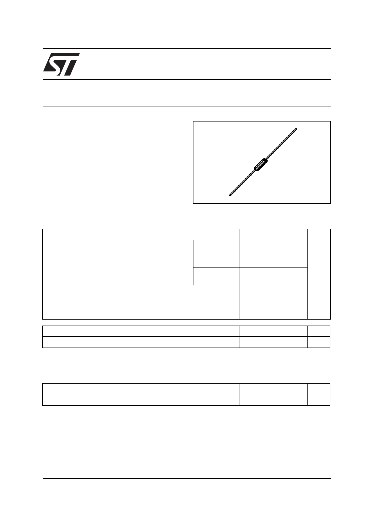
BYV 10- 40
DO 41
(Glass)
ABSOLUTE RATINGS
(limiting values)
Symbol Parameter Value Unit
I
F(AV)
I
FSM
T
stg
T
T
L
Average Forward Current*
Surge non Repetitive Forward Current
Storage and Junction Temperature Range - 65 to + 150
j
Maximum Lead Temperature for Soldering during 10s at 4mm
from Case
= 60
T
amb
= 25°C
T
amb
= 10ms
t
p
= 25°C
T
amb
t
= 300µs
p
C
°
Rectangular Pulse
1A
25
Sinusoidal Pulse
50
- 65 to + 125
230
Symbol Parameter BYV 10-40 Unit
V
RRM
* On infinite heatsink with 4mm lead length
Repetitive Peak Reverse Voltage 40 V
THERMAL RESISTANCE
Symbol Test Conditions Value Unit
R
th(j-a)
* On infinite heatsink with 4mm lead length
Junction-ambient* 110
C/W
°
A
C
°
C
°
C
°
August 1998 Ed : 1A
1/4
Page 2
BYV 10-40
ELECTRICAL CHARACT E RISTI CS
ST ATIC CHARACTERISTICS
Symbol Test Conditions Min. Typ. Max. Unit
*
I
R
VF *I
* Pulse test: t
= 25°C
T
j
= 100°C
T
j
= 1A
F
I
= 3A 0.85
F
300µs δ < 2%
≤
p
.
V
= V
R
= 25°C
T
j
RRM
0.5 mA
10
0.55 V
DYNAMIC CHARACTERI STICS
Symbol Test Conditions Min. Typ. Max. Unit
C
= 25°C VR = 0
T
j
Forward current flow in a Schottky rectifier is due to
majority carrier conduction. So reverse recovery is
not affected by stored charge as in c onventional PN
junction diodes.
Nevertheless, when the device switches from forward biased condition to reverse blocking state,
This current depends only of diode capacitance and
external circuit impedance. Satisfactory circuit behaviour analysis may be performed assuming that
Schottky rectifier consists of an ideal diode in parallel with a variable capacitance equal to the junction capacitance (see fig. 5 page 4/4).
220 pF
current is required to charge the depletion capacitance of the diode.
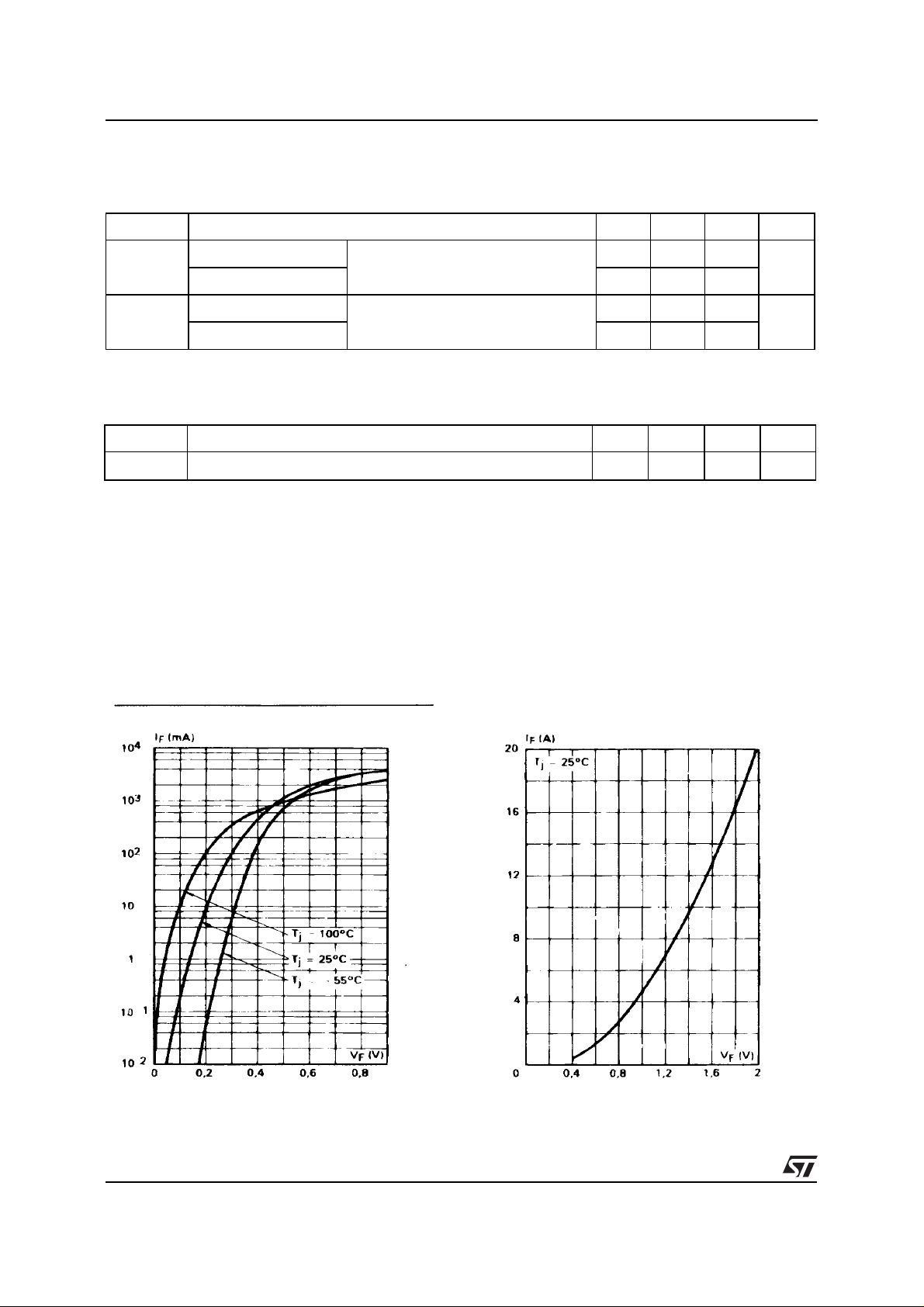
Fig.1 : Forward current versus forward
voltage at low level (typical values).
Fig.2 : Forward current versus forward
voltage at high level (typical values).
2/4
Page 3

BYV 10-40
Fig.3 : Reverse current versus junction
temperature.
Fig.4 : Reverse current versus V
cent.
RRM
in per
Fig.5 : Capacitance C versus reverse applied
voltage V
(typical values).
R
Fig.6 : Surge non repet itive f orwar d curre nt
for a rectangular pulse with t ≤ 10 ms.
3/4
Page 4

BYV 10-40
Figure 7. Surge non repetitive forward current
versus number of cycles.
PACKAGE MECHANICAL DATA
DO 41 Glass
REF . DIMENSIONS
CA
C
/
BO
Millimeters Inches
Min. Max. Min. Max.
A 4.07 5.20 0.160 0.205
B 2.04 2.71 0.080 0.107
O
/
D
O
/
D
C 28 1.102
D 0.712 0.863 0.028 0.034
Marking
: clear, ring at cathode end.
Cooling method : by convection and conduction
Weight: 0.33g
Information furnished is believed to be accurate and reliable. However, STMicroelectronics assumes no responsibility for the consequences of
use of such informat ion nor for any infringement of patent s or other rights of third parties which may result from its use. No license is granted
by implication or otherwise under any patent or patent rights of STMicroelectronics. Specifications mentioned in this publication are subject to
change without notice. This publication supersedes and replaces all information previously supplied.
STMicroelectronics products are not authorized for use as critical components in life support devices or systems without express written approval
of STMicroelectronic s.
The ST logo is a registered trademark of STMicroelectronics
© 1999 STMicroelectronics - Printed in Italy - All rights reserved.
Australia - Brazil - China - Finland - France - Germany - Hong Kong - India - Italy - Japan - Malaysia
Malta - Morocco - Singapore - Spain - Sweden - Switzerland - United Kingdom - U.S.A.
STMicroelectronics GROUP OF COMPANIES
http://www.st.com
4/4
 Loading...