

Page 1
BYT3400B(-TR)
®
October 1999 - Ed : 1C
FAST RECOV ERY REC T IFI ER DIO D E
I
F(AV)
3 A
V
RRM
400 V
V
F
(max) 1.4 V
MAIN PRODUCT CHARACTERISTIC S
VERY LOW REVERS E RECOVERY TIME
VERY LOW SWITCHING LOSSES
LOW NOISE TURN-OFF SWITCHING
SURFACE M OUNT P A CKAG E
TAPE AND REEL OPTION : -TR
FEATURES AND BENEFITS
Single high voltage rectifier suited to Switch Mode
Power Supplies and other power converters.
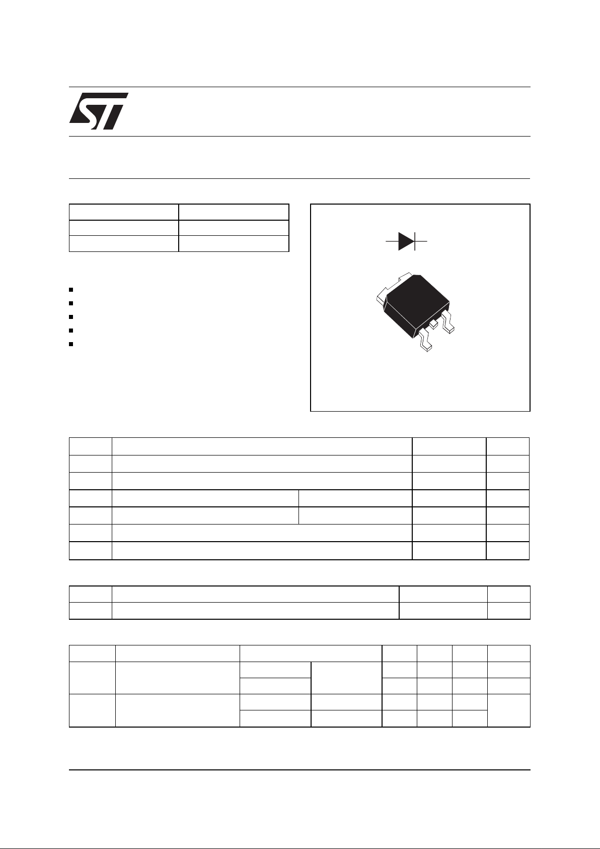
DESCR IPT ION
DPAK
(Plastic)
4
3
2
1 (nc)
Symbol Parameter Value Unit
V
RRM
Repetitive peak reverse voltage 400 V
I
F(RMS)
RMS forward current 10 A
I
F(AV)
Average forward current Tcase = ° C δ = 0.5 3 A
I
FSM
Surge non repetitive forward current tp = 10 ms Sinusoidal 60 A
Tstg Storage temperature range - 40 to + 150
°
C
Tj Maximum junction temperature 150 °C
ABSOLUTE MAXIMUM RATINGS
3
2, 4 (Tab)
Symbol Parameter Value Unit
R
TH (j-c)
Junction to case TBD
°
C/W
THERMAL RE SISTA NC ES
Symbol Tests Conditions Tests Conditions Min. Typ. Max. Unit
I
R
* Reverse leakage current Tj = 25°CV
R
= V
RRM
20
µ
A
Tj = 100°C0.5mA
V
F
** Forward voltage drop Tj = 25°CI
F
= 3 A 1.5 V
Tj = 100°CI
F
= 3 A 1.4
STATIC ELECTRICAL CHARACTER ISTICS
Pulse test : * tp = 5 ms, δ < 2 %
** tp = 380 µs, δ < 2%
1/3
Page 2
Symbol Test Conditions Min. Typ. Max. Unit
t
rr
Tj = 25°C IF = 0.5A
I
R
= 1A
Irr = 0.25A 25 ns
I
F
= 1A
V
R
= 30V
dI
F
/dt = -15 A/µs60ns
RECOVERY CHARACTE RISTICS
Symbol Test Conditions Min. Typ. Max. Unit
t
IRM
Vcc = 200V
Tj = 100°C
IF = 3A
dI
F
/dt = -50 A/µs
Lp ≤ 0.05µH3550ns
I
RM
1.5 2 A
To evaluate the maximum conduction losses use the following equation :
P = 1.1 x I
F(AV)
+ 0.08 I
F2(RMS)
TURN-OFF SWITCHING CHARACTERISTICS
BYT3400B(- TR)
2/3
Page 3

Information furnished is believed to be accurate and reliable. However, STMicroelectronics assumes no responsibility for the consequences of
use of such information nor for any infringement of patents or other rights of third parties which may result from its use. No license is granted by
implication or otherwi se under any pat ent or pat ent rights of STMi croelec tronics. Specificat ions ment ioned in this publicati on are subject to
change without notice. This publication supersedes and replaces all information previously supplied.
STMicroele ctroni cs products are not authoriz ed for use as critical compone nts in lif e support devices or system s without express writte n ap proval of STMicroelectronics.
The ST logo is a registered trad emark of STMicroelectr onics
© 1999 STMicroelectronics - Printed in Italy - All rights reserved.
STMicroelectronics GROUP OF COMPANIES
Australia - Brazil - China - Finland - France - Germany - Hong Kong - India - Italy - Japan - Malaysia
Malta - Morocco - Singapore - Spain - Sweden - Switzerland - United Kingdom - U.S.A.
http://www.st.com
FOOT PRINT
(in millimeters)
PACKAGE ME CHANICAL D AT A
DPAK
REF.
DIMENSIONS
Millimeters Inches
Min. Max Min. Max.
A 2.20 2.40 0.086 0.094
A1 0.90 1.10 0. 035 0.043
A2 0.03 0.23 0. 001 0.009
B 0.64 0.90 0.025 0.035
B2 5.20 5.40 0. 204 0.212
C 0. 45 0.60 0.017 0.023
C2 0.48 0.60 0.018 0.023
D 6. 00 6.20 0.236 0.244
E 6.40 6.60 0.251 0.259
G 4.40 4.60 0. 173 0.181
H 9. 35 10.10 0.368 0.397
L2 0.80 typ. 0.031 typ.
L4 0.60 1.00 0.023 0.039
V2 0° 8° 0° 8°
6.7
6.7
3
3
1.61.6
2.32.3
BYT3400B(-TR)
3/3
 Loading...