

Page 1
HIGH EFFICIENCY FAST RECOVERY DIODES
MAINPRODUCTCHARACTERISTICS
BYT30G-400
I
F(AV)
V
RRM
30 A
400 V
trr 50 ns
V
F
1.4 V
FEATURESAND BENEFITS
VERYLOWREVERSE RECOVERYTIME
VERYLOWSWITCHINGLOSSES
LOWNOISE TURN-OFFSWITCHING
SMDPACKAGE
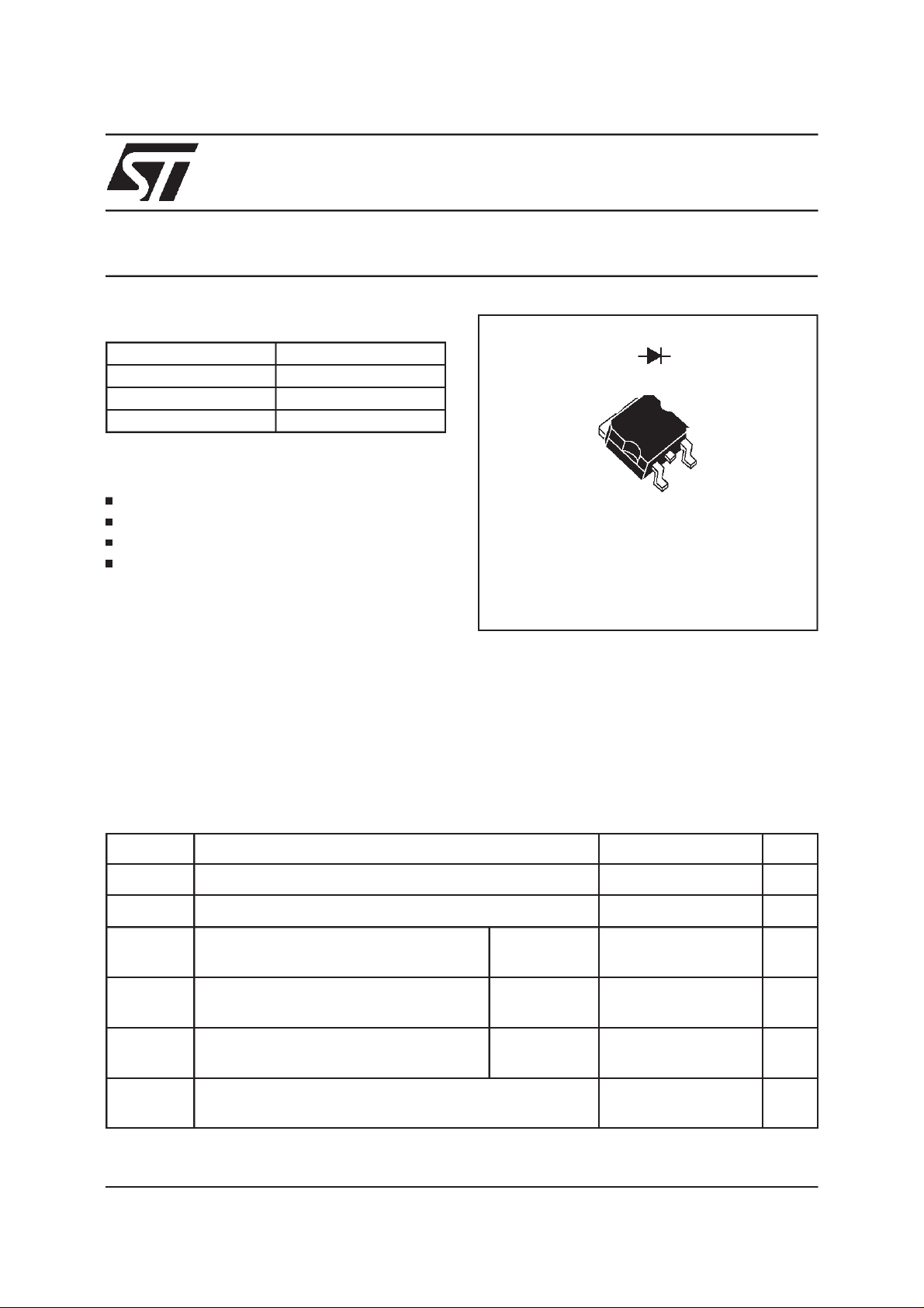
DESCRIPTION
Single rectifier suited for freewheelingin convertersand motor control circuits.
Packagedin D
2
PAK, this surface mount device is
intended for usein high frequencyinverters,free
wheelingand polarityprotectionapplications.
1&3 4
4
1
2
PAK
D
(Plastic)
2
3
ABSOLUTE MAXIMUM RATINGS
Symbol Parameter Value Unit
V
RRM
I
F(RMS)
I
F(AV)
Repetitivepeak reversevoltage 400 V
RMSforwardcurrent 50 A
Averageforwardcurrent Tc=100°C
30 A
δ =0.5
I
FSM
Surgenon repetitiveforwardcurrent tp=10ms
350 A
sinusoidal
I
FRM
Repetitivepeak forwardcurrent tp = 5µs
280 A
f = 5 kHz
Tstg
Storageand junctiontemperaturerange - 40 to+ 150
Tj
October 1999 - Ed: 3A
°
C
1/5
Page 2
BYT30G-400
THERMALRESISTANCE
Symbol Parameter Value Unit
Rth (j-c) Junctionto case 1 °C/W
STATICELECTRICALCHARACTERISTICS
Symbol Parameter TestConditions Min. Typ. Max. Unit
I
* Reverseleakagecurrent VR=V
R
V
F**
Pulse test : * tp = 5 ms, δ<2%
Forwardvoltagedrop IF=30A Tj=100°C 1.4 V
** tp = 380µs,δ<2%
RRM
I
=30A Tj=25°C 1.5
F
Toevaluate the conductionlossesuse the following equation:
P= 1.1x I
F(AV)
+0.0095 I
F2(RMS)
RECOVERYCHARACTERISTICS
Symbol Parameter TestConditions Min. Typ. Max. Unit
t
rr
Reverserecovery
time
Tj=25°CI
Irr = 0.25A I
Tj=25°C35µA
=100°C6mA
T
j
= 0.5A
F
=1A
R
50 ns
T
=25°CI
j
dI
/dt = -15A/µsVR=30V
F
=1A
F
100
TURN-OFF SWITCHINGCHARACTERISTICS
Symbol Parameter TestConditions Min. Typ. Max. Unit
t
IRM
I
RM
C factor Turn-off
PIN OUT configuration in D
Maximumreverse
recoverytime
Maximumreverse
recoverycurrent
overvoltage
coefficient
2
Tj=100°CdI
I
=30A dIF/dt = -240A/µs50
F
/dt = -120A/µs75ns
F
VCC= 200 V dIF/dt = -120A/µs9ns
Lp < 0.05 µHdI
=100°CI
T
j
/dt = -240A/µs12
F
F=IF(AV)
3.3 /
VCC=60V Lp=1µH
/dt = -30A/µs
dI
F
PAK:
2/5
Page 3

BYT30G-400
Fig.1 : Average forward power dissipation versus
averageforwardcurrent.
P
F(av)(W)
55
50
45
40
35
30
25
20
=0.5
=0.2
=0.1
=0.05
=1
T
15
10
5
0
0 5 10 15 20 25 30 35 40
Fig.3 :
Forward voltage drop versus forward cur-
I
F(av)(A)
=tp/T
tp
rent (maximumvalues).
V
FM(V)
2.0
1.8
1.6
1.4
1.2
1.0
0.8
0.6
0.4
0.2
0.0
0.1 1 10 100
o
Tj=100 C
I
FM(A)
Fig.2: Peakcurrent versusformfactor.
I
M(A)
500
=tp/T
T
I
M
tp
450
400
350
300
P=20W
250
200
150
100
P=30W
P=40W
50
0
0.0 0.1 0.2 0.3 0.4 0.5 0.6 0.7 0.8 0.9 1.0
Fig.4 :
Relative variation of thermal impedance
junctionto case versuspulseduration.
K
1
Zth(j-c) (tp. )
K=
Rth(j-c)
0.5
0.2
0.1
0.001 0.01 0.1 1
=0.5
=0.2
=0.1
Single pulse
tp(s)
=tp/ T
T
tp
Fig.5 : Non repetitive surge peak forward current
versusoverload duration.
I
M(A)
250
200
150
100
IM
50
0
0.001 0.01 0.1 1
t
=0.5
t(s)
o
Tc=25 C
o
Tc=60 C
o
Tc=100 C
Fig.6 : Averagecurrent versus ambient tempera-
ture.(δ: 0.5)
I
F(av)(A)
35
30
=0.5
25
T
20
15
=tp/T
tp
10
5
o
Tamb( C)
0
0 20 40 60 80 100 120 140 160
Rth(j-a)=15 C/W
Rth(j-a)=Rth(j-c)
o
3/5
Page 4

BYT30G-400
Fig.7:
Fig.9:
Reverserecoverycharge versusdIF/dt.
Peakreverse currentversus dIF/dt.
Fig.8:
Fig.10 :
Forwardrecoverytimes versusdI
Peakforward voltageversusdI
F
F
/dt.
/dt.
Fig.11:
perature.
4/5
Dynamicparameters versus junction tem-
Page 5

PACKAGEMECHANICAL DATA
2
D
PAK(Plastic)
E
L2
L
L3
B2
B
G
* FLATZONE NO LESSTHAN2mm
C2
A1
M
BYT30G-400
DIMENSIONS
REF.
A
A 4.40 4.60 0.173 0.181
A1 2.49 2.69 0.098 0.106
A2 0.03 0.23 0.001 0.009
D
B 0.70 0.93 0.027 0.037
B2 1.14 1.70 0.045 0.067
C 0.45 0.60 0.017 0.024
C2 1.23 1.36 0.048 0.054
C
R
D 8.95 9.35 0.352 0.368
E 10.00 10.40 0.393 0.409
G 4.88 5.28 0.192 0.208
L 15.00 15.85 0.590 0.624
A2
L2 1.27 1.40 0.050 0.055
L3 1.40 1.75 0.055 0.069
*
V2
M 2.40 3.20 0.094 0.126
R 0.40typ. 0.016typ.
V2 0° 8° 0° 8°
Millimeters Inches
Min. Max. Min. Max.
FOOTPRINT
10.30
Informationfurnished isbelieved tobeaccurate and reliable. However, STMicroelectronics assumes no responsibilityfor the consequences of
use ofsuch information nor for any infringementof patentsor other rights of thirdparties which mayresult fromits use. No license is granted by
implication or otherwise under any patent or patent rights of STMicroelectronics. Specificationsmentioned in this publication are subject to
change withoutnotice.This publicationsupersedes andreplaces all information previouslysupplied.
STMicroelectronics products are not authorized for use as criticalcomponents in lifesupport devices or systems without express written approval of STMicroelectronics.
(inmillimeters)
16.90
5.08
1.30
3.70
8.90
The ST logo is a registered trademark of STMicroelectronics
1999STMicroelectronics - Printed in Italy - All rights reserved.
STMicroelectronics GROUP OF COMPANIES
Australia - Brazil - China - Finland - France - Germany - Hong Kong- India- Italy - Japan - Malaysia
Malta - Morocco - Singapore -Spain - Sweden - Switzerland- United Kingdom - U.S.A.
http://www.st.com
5/5
 Loading...