

Page 1
BYT230PIV-400
FAST RECOVERY RECTIFIER DIODES
MAIN PRODUCT CHARACTERISTICS
I
F(AV)
V
RRM
VF(max) 1.4 V
trr (max) 50 ns
FEATURES ANDBENEFITS
n VERY LOW REVERSE RECOVERY TIME
n VERY LOW SWITCHING LOSSES
n LOW NOISE TURN-OFF SWITCHING
n INSULATED PACKAGE: ISOTOP
Insulation voltage: 2500 V
Capacitance = 45 pF
Inductance < 5nH
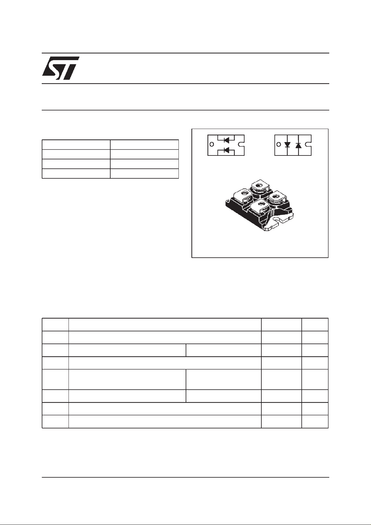
DESCRIPTION
2 x 30 A
400 V
RMS
BYT231PIV-400
K2 A2
A1K1
BYT231PIV-400
ISOTOP
(Plastic)
A2 K1
A1K2
BYT230PIV-400
TM
These rectifierdevicesaresuited for free-wheeling
function in converters and motor controlcircuits.
Packaged in ISOTOP, they are intended for use in
Switch Mode Power Supplies.
ABSOLUTE RATINGS (limiting values, per diode)
Symbol Parameter Value Unit
V
RRM
I
FRM
I
F(RMS)
I
F(AV)
Repetitive peakreverse voltage
Repetitive peakforward current tp=5 µs F=1kHz
RMS forward current
Average forward current Tc = 75°C
400 V
900 A
50 A
30 A
δ = 0.5
I
FSM
T
stg
Tj
TM: ISOTOP is aregistered trademark of STMicroelectronics.
Surge non repetitive forward current tp = 10 ms Sinusoidal
Storage temperaturerange
Maximum operating junction temperature
350 A
- 40 to + 150 °C
150 °C
May 2000 - Ed: 5D
1/6
Page 2

BYT230PIV-400 / BYT231PIV-400
THERMAL RESISTANCES
Symbol Parameter Value Unit
R
th(j-c)
Junction to case Per diode
Total
R
th(c)
Coupling
When the diodes 1 and 2 are used simultaneously :
∆ Tj(diode 1)= P(diode) x R
(Per diode) + P(diode 2) x R
th(j-c)
th(c)
STATIC ELECTRICAL CHARACTERISTICS (per diode)
Symbol Parameter Test Conditions Min. Typ. Max. Unit
VF*
Forward voltage drop Tj = 25°CI
=30A
F
Tj = 100°C
IR**
Pulse test : * tp = 380 µs, δ <2%
Reverse leakage current
** tp = 5 ms, δ <2%
Tj = 25°CV
R=VRRM
Tj = 100°C
To evaluatethe conduction losses use the following equation:
P = 1.1 x I
F(AV)
+0.0095 I
F2(RMS)
1.5
0.8
0.1
°C/W
1.5 V
1.4
35 µA
6mA
RECOVERY CHARACTERISTICS
Symbol Test Conditions Min. Typ. Max. Unit
t
rr
Tj = 25°CIF=1A VR= 30V dIF/dt = - 15A/µs
IF= 0.5A IR=1A Irr= 0.25A
100 ns
50
TURN-OFF SWITCHING CHARACTERISTICS
Symbol Parameter Test Conditions Min. Typ. Max. Unit
t
C=
IRM
I
RM
V
V
Maximum reverse
recovery time
Maximum reverse
recovery current
Turn-off overvol t age
RP
coeff icient
CC
dIF/dt = - 120 A/µsV
dIF/dt = - 240 A/µs
dIF/dt = - 120 A/µs
dIF/dt = - 240 A/µs
Tj = 100°CVCC= 60V IF=I
= 200 V
CC
IF=30A
Lp0.05 µH
Tj = 100°C
(see fig. 13)
F(AV)
dIF/dt = - 30A/µsLp=1µH
(see fig. 14)
75 ns
50
9A
12
3.3 /
2/6
Page 3

BYT230PIV-400 / BYT231PIV-400
Fig. 1: Average forward power dissipation versus
average forward current (per diode).
PF(av)(W)
60
50
40
δ= 0.2
δ = 0.1
δ = 0.05
δ=0.5
δ =1
30
20
T
10
0
IF(av)(A)
0 5 10 15 20 25 30 35 40
δ
=tp/T
tp
Fig. 3: Average forward current versus ambient
temperature (δ=0.5, per diode).
IF(av)(A)
35
30
25
20
15
10
5
=tp/T
δ
0
0 25 50 75 100 125 150
T
Rth(j-a)=Rth(j-c)
tp
Rth(j-a)=5°C/W
Tamb(°C)
Fig. 2:Peak currentversus form factor (per diode).
IM(A)
250
T
200
=tp/T
150
100
50
0
0.0 0.1 0.2 0.3 0.4 0.5 0.6 0.7 0.8 0.9 1.0
P=40W
P=50W
P=30W
P=20W
δ
δ
tp
Fig. 4: Non repetitive surge peak forward current
versus overload duration (per diode).
IM(A)
200
180
160
140
120
100
80
IM
60
40
1E-3 1E-2 1E-1 1E+0
δ=0.5
t
Tc=50°C
Tc=25°C
Tc=75°C
t(s)
Fig. 5: Relative variation of thermal impedance
junction tocase versus pulse duration (per diode).
K=[Zth(j-c)/Rth(j-c)]
1.0
δ =0.5
0.5
δ =0.2
δ =0.1
0.2
Single pulse
0.1
1E-3 1E-2 1E-1 1E+0
tp(s)
δ
=tp/T
T
tp
Fig. 6: Forward voltage drop versus forward
current (maximumvalues, per diode).
IFM(A)
200.0
100.0
10.0
1.0
0.1
0.0 0.5 1.0 1.5 2.0 2.5
Typicalvalues
Tj=100°C
Tj=25°C
Tj=100°C
VFM(V)
3/6
Page 4

BYT230PIV-400 / BYT231PIV-400
Fig. 7: Junction capacitance versus reverse
voltage applied (typical values, per diode).
C(pF)
100
90
F=1MHz
Tj=25°C
80
70
60
50
40
30
20
1 10 100 200
VR(V)
Fig. 9: Recovery current versus dIF/dt (per diode).
IRM(A)
50
IF=IF(av)
90% confidence
Tj=100°C
Fig. 8: Recovery charges versus dIF/dt (per
diode).
Qrr(nC)
1000
IF=IF(av)
90% confidence
Tj=100°C
100
dIF/dt(A/µs)
10
10 20 50 100 200 500
Fig. 10: Transient peak forward voltage versus
dIF/dt (per diode).
VFP(V)
30
IF=IF(av)
90% confidence
Tj=100°C
25
10
dIF/dt(A/µs)
1
10 20 50 100 200 500
Fig. 11: Forward recovery time versus dIF/dt (per
diode).
tfr(µs)
1.50
1.25
1.00
0.75
0.50
0.25
0.00
0 100 200 300 400 500
dIF/dt(A/µs)
IF=IF(av)
90% confidence
Tj=100°C
20
15
10
5
0
0 100 200 300 400 500
dIF/dt(A/µs)
Fig. 12: Dynamic parameters versus junction
temperature.
Qrr;IRM[Tj] / Qrr;IRM[Tj=100°C]
1.50
1.25
1.00
0.75
0.50
0.25
0 25 50 75 100 125 150
IRM
Qrr
Tj(°C)
4/6
Page 5

BYT230PIV-400 / BYT231PIV-400
Fig. 13: Turn-off switching characteristics (without
serie inductance).
IF
LC
DUT
VCC
VF
IRM
diF/dt
VCC
tIRM
Fig. 14: Turn-off switching characteristics (with
serie inductance).
IF
LC
DUT
LP
VCC
VF
VRP
diF/dt
VCC
5/6
Page 6

BYT230PIV-400 / BYT231PIV-400
PACKAGE MECHANICAL DATA
ISOTOP
DIMENSIONS
REF.
Millimeters Inches
Min. Max. Min. Max.
A 11.80 12.20 0.465 0.480
A1 8.90 9.10 0.350 0.358
B 7.8 8.20 0.307 0.323
C 0.75 0.85 0.030 0.033
C2 1.95 2.05 0.077 0.081
D 37.80 38.20 1.488 1.504
D1 31.50 31.70 1.240 1.248
E 25.15 25.50 0.990 1.004
E1 23.85 24.15 0.939 0.951
E2 24.80 typ. 0.976 typ.
G 14.90 15.10 0.587 0.594
G1 12.60 12.80 0.496 0.504
G2 3.50 4.30 0.138 0.169
F 4.10 4.30 0.161 0.169
F1 4.60 5.00 0.181 0.197
P 4.00 4.30 0.157 0.69
P1 4.00 4.40 0.157 0.173
S 30.10 30.30 1.185 1.193
Ordering type Marking Package Weight Base qty
Delivery
mode
BYT230PIV-400 BYT230PIV-400 ISOTOP 28 g. (without screws) 10 Tube
BYT231PIV-400 BYT231PIV-400 ISOTOP 28 g. (without screws) 10 Tube
n Cooling method: by conduction (C)
n Recommended torque value : 1.3 N.m (MAX 1.5 N.m) for the 6 x M4 screws. (2 x M4 screws recom-
mended for mounting the package on the heatsink and the 4 screws given with the screw version).The
screws supplied with the package are adapted for mounting on a board (or other types of terminals) with
a thickness of 0.6 mm min and 2.2 mm max.
n Epoxy meets UL94,V0
Information furnished is believedtobeaccurateandreliable.However,STMicroelectronicsassumesnoresponsibility for the consequencesof
use of such informationnor forany infringementofpatents or otherrights of third parties which may result from its use. No license is granted by
implication or otherwise under any patent or patent rights of STMicroelectronics. Specifications mentioned in this publication are subject to
change withoutnotice. This publication supersedes and replaces all information previously supplied.
STMicroelectronics products are not authorized for use as critical components in life support devices or systems without express written approval of STMicroelectronics.
The ST logo is a registered trademark of STMicroelectronics
2000 STMicroelectronics - Printed in Italy - All rights reserved.
STMicroelectronics GROUP OF COMPANIES
Australia - Brazil - China - Finland - France - Germany - Hong Kong - India - Italy - Japan - Malaysia
Malta - Morocco - Singapore - Spain - Sweden - Switzerland - United Kingdom - U.S.A.
http://www.st.com
6/6
 Loading...