

Page 1
BYT230Y-400
FAST RECOVERY RECTIFIERDIODES
PRELIMINARY DATASHHET
MAINPRODUCTCHARACTERISTICS
I
F(AV)
V
RRM
2 x 30 A
400 V
Tj (max) 150°C
(max) 1.3 V
V
F
FEATURESAND BENEFITS
VERYLOWREVERSERECOVERYTIME
VERYLOWSWITCHINGLOSSES
LOWNOISETURN-OFF SWITCHING
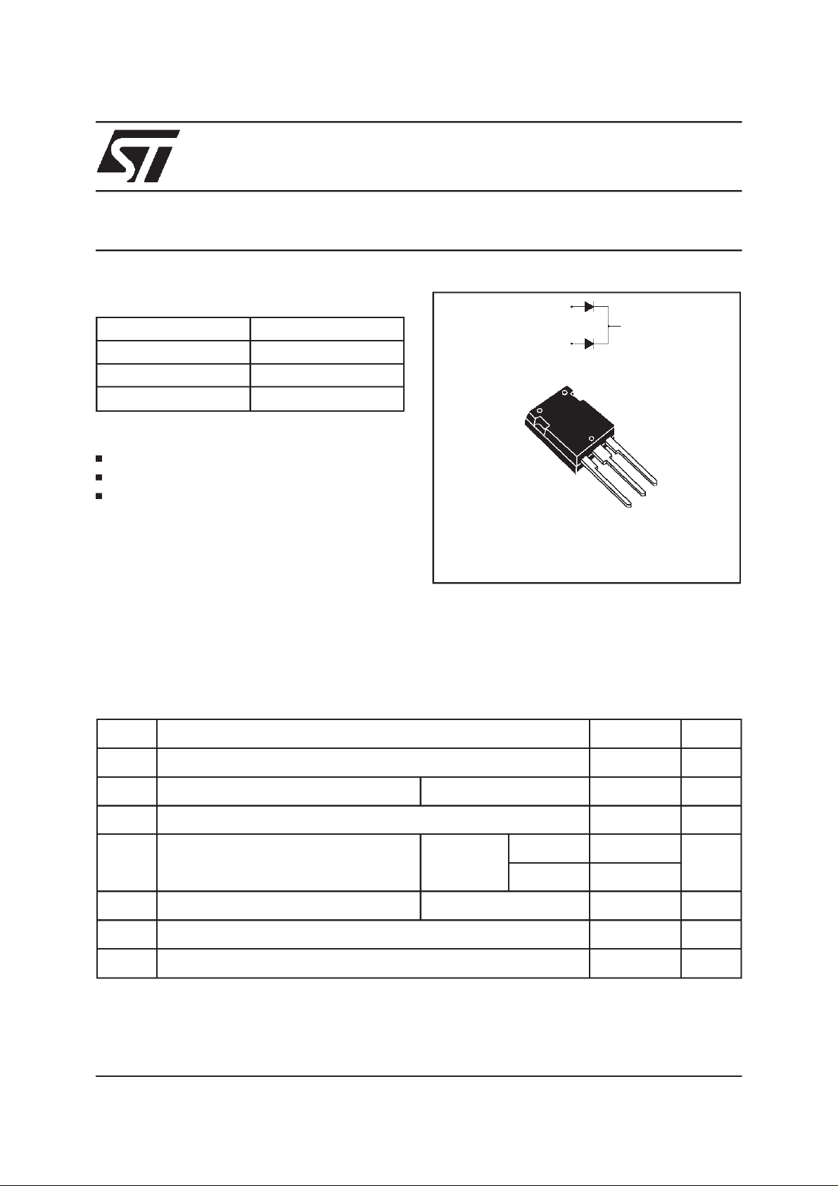
DESCRIPTION
Dual400Vrectifierssuitedfor SwitchModePower
Suppliesand other converters.
Packagedin Max247, this device is also intended
for use in welding equipment and telecom power
supplies.
ABSOLUTE RATINGS
(limitingvalues,perdiode)
A1
K
A2
A2
K
A1
Max247
Symbol Parameter Value Unit
V
RRM
I
FRM
I
F(RMS)
I
F(AV)
I
FSM
T
stg
Tj
October 1999 - Ed: 3A
Repetitivepeakreverse voltage
Repetitivepeakforward current tp=5µs F=5kHz
RMSforwardcurrent
Averageforward current Tc= 105°C
Surgenonrepetitiveforwardcurrent tp= 10 ms Sinusoidal
Storagetemperature range
Maximumoperating junctiontemperature
Per diode
δ = 0.5
Per device
400 V
380 A
50 A
30 A
60
300 A
- 55 to + 150 °C
150 °C
1/5
Page 2
BYT230Y-400
THERMAL RESISTANCES
Symbol Parameter Value Unit
R
R
th (j-c)
th(c)
Junctionto case Perdiode
Total
Coupling
0.95
0.55
0.15 °C/W
Whenthe diodes1 and 2 are used simultaneously:
∆ Tj(diode1) = P(diode1)x R
(Perdiode) + P(diode2) x R
th(j-c)
th(c)
STATICELECTRICALCHARACTERISTICS(per diode)
Symbol Parameter Tests Conditions Min. Typ. Max. Unit
I
*
R
Reverseleakage
current
V
**
F
Pulse test : * tp = 5 ms,δ<2%
Forwardvoltagedrop Tj= 25°CI
** tp = 380 µs, δ <2%
Tj= 25°CV
R=VRRM
Tj= 125°C
=30A
F
Tj= 125°CI
Tj= 25°CI
Tj= 125°CI
=30A
F
=60A
F
=60A
F
312mA
0.9 1.3
1.1 1.6
35 µA
1.5 V
1.7
°C/W
To evaluatethe conductionlossesuse the followingequation:
P = 1.0x I
F(AV)
+ 0.01 I
F2(RMS)
RECOVERYCHARACTERISTICS
Symbol TestConditions Min. Typ. Max. Unit
t
rr
Tj=25°CIF= 0.5A IR=1A Irr=0.25A
I
=1A VR= 30V dIF/dt= - 15A/µs
F
50 ns
100
TURN-OFFSWITCHINGCHARACTERISTICS (without serieinductance)
Symbol TestConditions Min. Typ. Max. Unit
t
I
IRM
RM
dIF/dt = - 120A/µsV
/dt = - 240A/µs
dI
F
dIF/dt = - 120A/µs
dI
/dt = - 240A/µs
F
CC
= 30A
I
F
=0.05µH
L
p
T
= 100°C
j
=200 V
50
12
75 ns
9A
TURN-OFFOVERVOLTAGECORFFICIENT (withserie inductance)
Symbol TestConditions Min. Typ. Max. Unit
3.3 /
C=
V
V
Tj=100°CVCC= 60V IF=I
RP
dIF/dt = - 30A/µsLp=1µH
CC
F (AV)
2/5
Page 3

BYT230Y-400
Fig. 1: Average forward power dissipation versus
averageforward current (per diode).
PF(av)(W)
60
δ = 0.5
50
δ = 0.1
δ = 0.05
δ = 0.2
δ =1
40
30
20
T
10
=tp/T
0
0 5 10 15 20 25 30 35 40
IF(av)(A)
δ
tp
Fig. 3: Average forward current versus ambient
temperature(δ=0.5, perdiode).
IF(av)(A)
35
30
25
20
15
10
5
=tp/T tp
δ
0
0 25 50 75 100 125 150
Rth(j-a)=Rth(j-c)
Rth(j-a)=5°C/W
T
Tamb(°C)
Fig.2: Peakcurrent versusform factor(per diode).
IM(A)
250
P=40W
T
200
=tp/T tp
δ
150
P=60W
100
P=20W
50
0
0.0 0.1 0.2 0.3 0.4 0.5 0.6 0.7 0.8 0.9 1.0
P=80W
Fig. 4: Non repe ti t i ve surge peak forward current
versusoverloadduration( perdiode).
IM(A)
250
200
150
Tc=50°C
100
IM
50
0
1E-3 1E-2 1E-1 1E+0
δ=0.5
t
t(s)
Tc=75°C
Tc=110°C
Fig. 5: Relative variation of thermal impedance
junctionto case versuspulse duration (perdiode).
K=[Zth(j-c)/Rth(j-c)]
1.0
δ= 0.5
δ= 0.2
δ = 0.1
Single pulse
tp(s)
0.1
1E-3 1E-2 1E-1 1E+0
T
=tp/T tp
δ
Fig. 6:
Forward voltage drop versus forward
current(maximumvalues, per diode).
IFM(A)
200.0
100.0
10.0
1.0
0.1
0.0 0.5 1.0 1.5 2.0 2.5
Typicalvalues
Tj=125°C
Tj=25°C
Tj=125°C
VFM(V)
3/5
Page 4

BYT230Y-400
Fig. 7:
Junction capacitance versus reverse
voltageapplied(typicalvalues, per diode).
C(pF)
100
50
20
10
1 10 100 200
Fig.9:
50
Recoverycurrentversus dI
IRM(A)
IF=IF(av)
90% confidence
Tj=100°C
VR(V)
/dt (perdiode).
F
F=1MHz
Tj=25°C
Fig.8:
Fig. 10:
RecoverychargesversusdI
Qrr(nC)
1000
100
IF=IF(av)
90% confidence
Tj=100°C
10
10 20 50 100 200 500
dIF/dt(A/µs)
Transientpeak forwardversusdI
/dt(perdiode).
F
diode).
VFP(V)
30
25
IF=IF(av)
90% confidence
Tj=100°C
/dt(per
F
10
1
10 20 50 100 200 500
Fig. 11:
Forward recoverytime versusdI
dIF/dt(A/µs)
/dt (per
F
diode).
tfr(µs)
1.50
1.25
1.00
0.75
0.50
0.25
0.00
0 100 200 300 400 500
dIF/dt(A/µs)
IF=IF(av)
90% confidence
Tj=100°C
20
15
10
5
0
0 100 200 300 400 500
Fig. 12:
Dynamic parameters versus junction
dIF/dt(A/µs)
temperature.
Qrr;IRM[Tj] / Qrr;IRM[Tj=100°C]
1.50
1.25
1.00
0.75
0.50
0.25
0 25 50 75 100 125 150
IRM
Qrr
Tj(°C)
4/5
Page 5

PACKAGEMECHANICAL DATA
Max247
BYT230Y-400
DIMENSIONS
REF.
Millimeters Inches
Min. Max. Min. Max.
AE
A 4.70 5.30 0.185 0.209
A1 2.20 2.60 0.087 0.102
b 1.00 1.40 0.038 0.055
D
b1 2.00 2.40 0.079 0.094
b2 3.00 3.40 0.118 0.133
c 0.40 0.80 0.016 0.031
L1
D 19.70 10.30 0.776 0.799
A1
e 5.35 5.55 0.211 0.219
b1
L
b2
e
b
c
E 15.30 15.90 0.602 0.626
L 14.20 15.20 0.559 0.598
L1 3.70 4.30 0.146 0.169
Orderingtype Marking Package Weight Base qty Deliverymode
BYT230Y-400 BYT230Y-400 Max247 5g. 30 Tube
EpoxymeetsUL94,V0
Informationfurnishedis believed to beaccurateand reliable. However, STMicroelectronics assumes no responsibilityfor theconsequences of
use of such informationnor forany infringementof patents or otherrights of thirdparties which may result fromits use. No license is granted by
implication or otherwise under any patent or patent rights of STMicroelectronics. Specifications mentioned in this publication are subject to
change without notice. This publication supersedes and replaces all information previously supplied.
STMicroelectronics products are not authorized for use as critical components in life support devices or systems without express written approval of STMicroelectronics.
The ST logo is a registered trademark of STMicroelectronics
1999 STMicroelectronics- Printed inItaly - All rights reserved.
STMicroelectronics GROUP OF COMPANIES
Australia -Brazil - China - Finland - France - Germany - Hong Kong - India - Italy -Japan - Malaysia
Malta - Morocco - Singapore - Spain - Sweden - Switzerland - United Kingdom - U.S.A.
http://www.st.com
5/5
 Loading...