

Page 1
ULTRAFAST POWER RECTIFIER DIODE
MAIN PRODUCT CHARACTERISTICS
BYT200PIV-400
I
F(AV)
V
RRM
2 x100 A
400 V
VF(max) 1.4 V
FEATURES AND BENEFITS
n LOW CONDUCTION LOSSES
n NEGLIGIBLE SWITCHING LOSSES
n HIGH AVALANCHE CAPABILITY
n ISOLATED PACKAGE :
2500 V
DC
CAPACITANCE 42pF
DESCRIPTION
High current power rectifier diode suited for
Switched Mode Power Supply and high frequency
DC to DC converters.
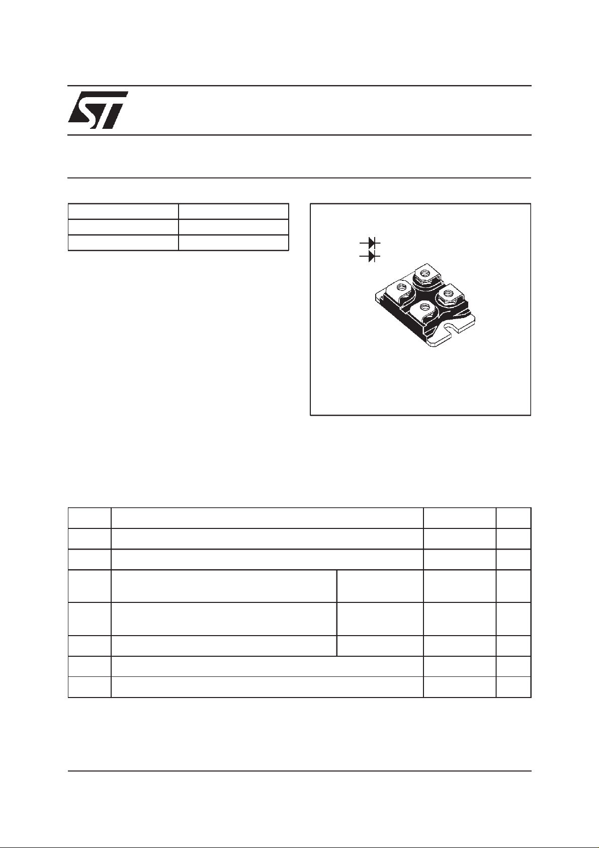
Packaged in ISOTO P, this devic e is intended
for use in a medi um v olt age hig h c ur rent applications such as welding equipment and
Telecom supplies.
ABSOLUTE MAXIMUM RATING
A1 K1
A2 K2
4
ISOTOP
1=A1
2
3
TM
2=K1
3=A2
4=K2
1
Symbol Parameter Value Unit
V
RRM
I
F(RMS)
I
F(AV)
Repetitive peak reverse voltage 400 V
RMS forward current 150 A
Average forward current Tc = 80°C
100 A
δ = 0.5
I
FSM
Surge non repetitive forward current tp = 10 ms
600 A
Sinusoidal
I
FRM
T
stg
Repetitive peak forward current tp 10 µs 800 A
Storage temperature range - 40 to + 150 °C
Tj Maximum junction temperature 150 °C
ISOTOP is atrademark of STMicroelectronics
May 2000 - Ed: 3C
1/5
Page 2

BYT200PIV-400
THERMAL RESISTANCES
Symbol Parameter Value Unit
R
th (j-c)
R
th (c)
STATIC ELECTRICAL CHARACTERISTICS (per diode)
Symbol Parameter Tests Conditions Min. Typ. Max. Unit
IR* Reverse leakage current Tj = 25°CV
VF** Forward voltage drop Tj = 25°CI
Pulse test : * tp = 5 ms, duty cycle < 2 %
RECOVERY CHARACTERISTICS
Junction to case Per leg 0.55 °C/W
Total 0.33
Coupling 0.1
R=VRRM
120 µA
Tj = 100°C 4 12 mA
= 100 A 1.6 V
F
Tj = 125°CI
** tp = 380 µs, duty cycle < 2%
= 100 A 0.95 1.4
F
Symbol Parameter Test Conditions Min. Typ. Max. Unit
t
rr
Reverse recovery time IF=0.5A IR=1A Irr=0.25A
IF=1A dI/dt= -50A/µs
55
100
Vr=30V
I
RM
Reverserecoverycurrent dIF/dt=-200A/µs Tj=125°C
40 A
VR=400V IF=100A
S factor Softness factor dIF/dt=-200A/µs Tj=125°C
0.25
VR=400V IF=100A
t
fr
Forward recovery time IF=100A dIF/dt=500A/µs
500 ns
Measured at 1.1 x VFmax.
V
FP
Peak forward voltage 12 V
Tj=25°C
To evaluate the conduction losses use the following equation :
P = 0.8 x I
+ 0.00228 x I
F(AV)
F2(RMS)
ns
2/5
Page 3

BYT200PIV-400
Fig. 1: Average forward power dissipation versus
average forward current (per diode).
PF(av)(W)
140
120
100
80
δ = 0.2
δ= 0.1
δ = 0.05
δ = 0.5
δ =1
60
40
20
0
0 102030405060708090100110120130
IF(av)(A)
Fig. 3: Average forward current versus ambient
temperature (δ = 0.5, per diode).
IF(av)(A)
120
100
80
60
40
20
0
0 25 50 75 100 125 150
Rth(j-a)=Rth(j-c)
Rth(j-a)=2°C/W
Tamb(°C)
Fig. 2:Peak currentversus form factor(perdiode).
IM(A)
500
400
300
200
P=75W
P=100W
P=125W
P=150W
100
0
0.0 0.1 0.2 0.3 0.4 0.5 0.6 0.7 0.8 0.9 1.0
δ
Fig. 4: Non repetitive surge peak forward current
versus overload duration (per diode).
IM(A)
700
600
500
400
300
200
100
0
1E-3 1E-2 1E-1 1E+0
t(s)
Tc=50°C
Tc=75°C
Tc=100°C
Fig. 5: Relative variation of thermal impedance
junction to case versus pulse duration (per diode).
K=[Zth(j-c)/Rth(j-c)]
1.0
δ = 0.5
0.5
δ = 0.2
δ = 0.1
0.2
Single pulse
0.1
1E-3 1E-2 1E-1 1E+0
tp(s)
Fig. 6: Forwardvoltage drop versus forward current
(maximumvalues,perdiode).
IFM(A)
500
100
10
1
0.50 0.75 1.00 1.25 1.50 1.75 2.00 2.25 2.50
Tj=125°C
Tj=25°C
VFM(V)
3/5
Page 4

BYT200PIV-400
Fig. 7: Junctioncapacitance versusreversevoltage
applied(typicalvalues, perdiode).
C(pF)
500
450
F=1MHz
Tj=25°C
400
350
300
250
200
150
100
1 10 100 200
VR(V)
Fig. 9:Recovery current versusdIF/dt(perdiode).
IRM(A)
50
IF=IF(av)
90% confidence
45
Tj=125°C
40
35
30
25
20
15
10
5
0
0 100 200 300 400 500
dIF/dt(A/µs)
Fig. 8: Recoverycharges versusdIF/dt(perdiode).
Qrr(µC)
3.0
2.5
IF=IF(av)
90% confidence
Tj=125°C
2.0
1.5
1.0
0.5
0.0
0 100 200 300 400 500
dIF/dt(A/µs)
Fig. 10: Transient peak forward voltage versus
dIF/dt (per diode).
VFP(V)
14
IF=IF(av)
90% confidence
12
Tj=125°C
10
8
6
4
2
0
0 100 200 300 400 500 600 700 800
dIF/dt(A/µs)
Fig. 11: Dynam ic parameters versus junction
temperature.
Qrr;IRM[Tj] / Qrr;IRM[Tj=125°C]
1.25
1.00
0.75
0.50
0.25
0.00
0 25 50 75 100 125 150
4/5
IRM
Qrr
Tj(°C)
Page 5

PACKAGE MECHANICAL DATA
ISOTOP
BYT200PIV-400
DIMENSIONS
REF.
A 11.80 12.20 0.465 0.480
A1 8.90 9.10 0.350 0.358
B 7.8 8.20 0.307 0.323
C 0.75 0.85 0.030 0.033
C2 1.95 2.05 0.077 0.081
D 37.80 38.20 1.488 1.504
D1 31.50 31.70 1.240 1.248
E 25.15 25.50 0.990 1.004
E1 23.85 24.15 0.939 0.951
E2 24.80 typ. 0.976 typ.
G 14.90 15.10 0.587 0.594
G1 12.60 12.80 0.496 0.504
G2 3.50 4.30 0.138 0.169
F 4.10 4.30 0.161 0.169
F1 4.60 5.00 0.181 0.197
P 4.00 4.30 0.157 0.69
P1 4.00 4.40 0.157 0.173
S 30.10 30.30 1.185 1.193
Millimeters Inches
Min. Max. Min. Max.
n Epoxy meets UL94, V0
Information furnished is believed to beaccurate andreliable. However, STMicroelectronicsassumes noresponsibilityfor the consequencesof
use ofsuch information norfor any infringementof patentsorother rights of thirdparties whichmay result from its use. Nolicenseis grantedby
implication or otherwise under any patent or patent rights of STMicroelectronics. Specifications mentioned in this publication are subject to
change without notice.This publication supersedes and replaces all information previously supplied.
STMicroelectronics products are not authorized for use as critical componentsin life support devices orsystems without express written approval of STMicroelectronics.
The ST logo is a registered trademark of STMicroelectronics
2000 STMicroelectronics - Printed in Italy - All rights reserved.
STMicroelectronics GROUP OF COMPANIES
Australia - Brazil - China - Finland - France - Germany - Hong Kong - India - Italy - Japan - Malaysia
Malta - Morocco - Singapore - Spain - Sweden - Switzerland - United Kingdom - U.S.A.
http://www.st.com
5/5
 Loading...