

Page 1
®
SOFT RECOVERY
VERY HIGH VOLTAGE
SMALL RECOVERY CHARGE
BYT 13-600 →1000
FAST RECOVERY RECTIFIER DIODES
APPLICATIONS
ANTISATURATION DIODES FOR TRANSIS-
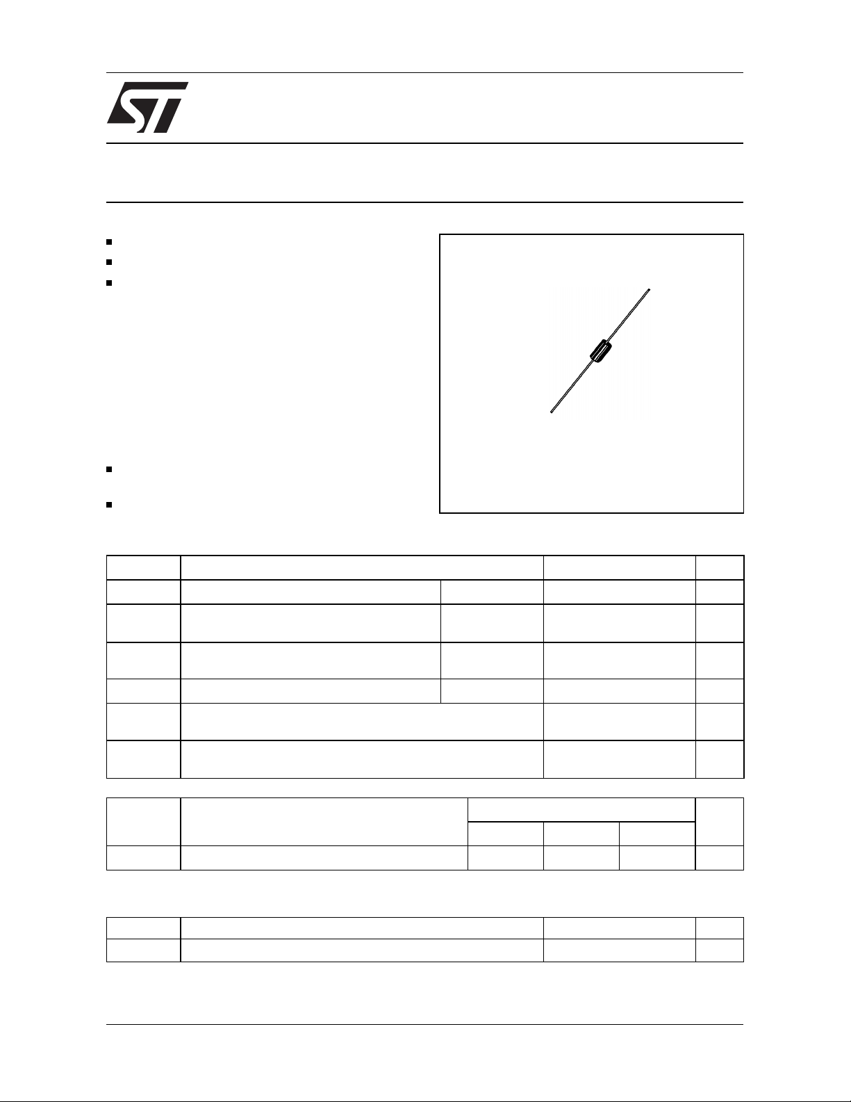
DO-201AD
(Plastic)
TOR BASE D RIVE
SNUBBER DIODES
ABSOLUTE MAXIMU M RATINGS
Symbol Parameter Value Unit
I
FRM
I
F (AV)
I
FSM
P
tot
T
stg
T
T
L
Symbol Parameter
V
RRM
Repetive Peak Forward Current
Average Forward Current * T
Surge non Repetitive Forward Current tp = 10ms
Power Dissipation *
Storage and Junction Temperature Range - 40 to + 150
j
Maximum Lead Temperature for Soldering during 10s at 4mm
from Case
Repetitive Peak Reverse Voltage 600 800 1000 V
(limiting values)
≤ 20µs
t
p
55°C
a =
= 0.5
δ
Sinusoidal
55°C
T
a =
50 A
3A
100 A
3.75 W
- 40 to + 150
230
BYT 13-
600 800 1000
C
°
C
°
Unit
THERMAL RESIST ANCE
Symbol Parameter Value Unit
R
th (j - a)
* On infinite heatsink with 10mm lead length.
August 1998 Ed : 1B
Junction-ambient* 25
C/W
°
1/4
Page 2
BYT13-600 → 1000
ELECTRICAL CHARACTERISTICS
STATIC CHARACTERISTICS
Synbol Test Conditions Min. Typ. Max. Unit
I
R
V
F
Tj = 25°C
Tj = 25°C
RECOVERY CHARACTERISTICS
Symbol Test Conditions Min. Typ. Max. Unit
V
= V
R
RRM
I
= 3A 1.3 V
F
20
A
µ
t
rr
Tj = 25°C IF = 0.5A IR = 1A Irr = 0.25A
To eva luate the conduction losses use the following equations:
V
= 0.95 + 0.050 IF P = 0.95 x I
F
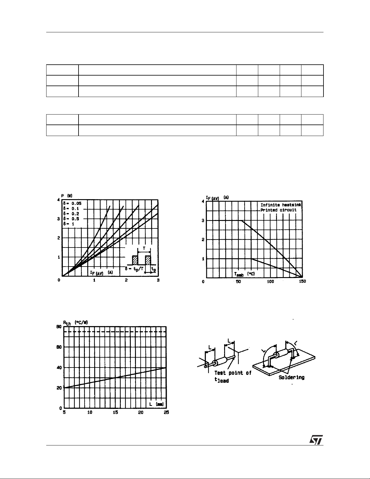
Figure 1. Maximum average power
dissipation versus average forward current.
F(AV)
+ 0.050 I
Figure 2. Average forward current versus
ambient temperature.
F2(RMS)
150 ns
Figure 3. Thermal resistance versus lead
length.
2/4
Mounting n°1
INFINITE HEATSINK
Mounting n°2
PRINTED CIRCUIT
Page 3

BYT 13-600 → 1000
Figure 4. Transient thermal impedance
junction-ambient for mounting n°2 versus
pulse duration (L = 10 mm).
Figure 5. Peak forward current
versus peak forward voltage drop
(maximum values).
Figure 6. Capacitance versus reverse applied
voltage
Figure 7. Non repetitive surge peak current
versus number of cycles
3/4
Page 4

BYT13-600 → 1000
PACKAGE MECHANICAL DATA
DO-201AD (Plastic)
BA
B
ØC
note 1
E
ØD ØD
note 2
note 1
E
REF. DIMENSIONS NOTES
Millimeters Inches
Min. Max. Min. Max.
A 9.50 0.374
B 25. 40 1.000
∅
∅
C
D
5.30 0.209
1.30 0.051
1 - The lead diameter ∅ D is not controlled over zone E
2 - The minimum axial lengh within which the device may be
placed with its leads bent at right angles is 0.59"(15 mm)
E 1.25 0.049
Marking
: type number, white band indicates cathode
Cooling method : by convection (method A)
Weight : 1.166g
Information furnished is believed to be accurate and reliable. However, STMicroelect ronics assum es no responsIbility for the consequences
of use of such information nor for any infringement of patents or other rights of third parties which may result from its use. No license is granted
by implication or otherwise under any patent or patent rights of STMicroelectronics. Specifications mentioned in this publication are subject to
change without notice. This publication supersedes and replaces all information previously supplied.
STMicroelectronics products are not authorized for use as critical components in life support devices or systems without express written approval
of STM i croel ectr o nics.
The ST logo is a registered trademark of STMicroelectronics
© 1998 STMicroelectronics - Printed in Italy - All rights reserved.
Australia - Brazil - Canada - China - France - Germany - Italy - Japan - Korea - Malaysia - Malta - Mexico - Morocco -
The Netherlands Singapore - Spain - Sweden - Switzerland - Taiwan - Thailand - United Kingdom - U.S.A.
STMicroelectronics GROUP OF COMPANIES
4/4
 Loading...