

Philips Semiconductors Objective specification
Rectifier diode BY359DX-1500
fast, high-voltage
FEATURES SYMBOL QUICK REFERENCE DATA
• Low forward volt drop VR = 1500 V
• Fast switching
• Soft recovery characteristic VF ≤ 1.5 V
• High thermal cycling performance
• Isolated mounting tab I
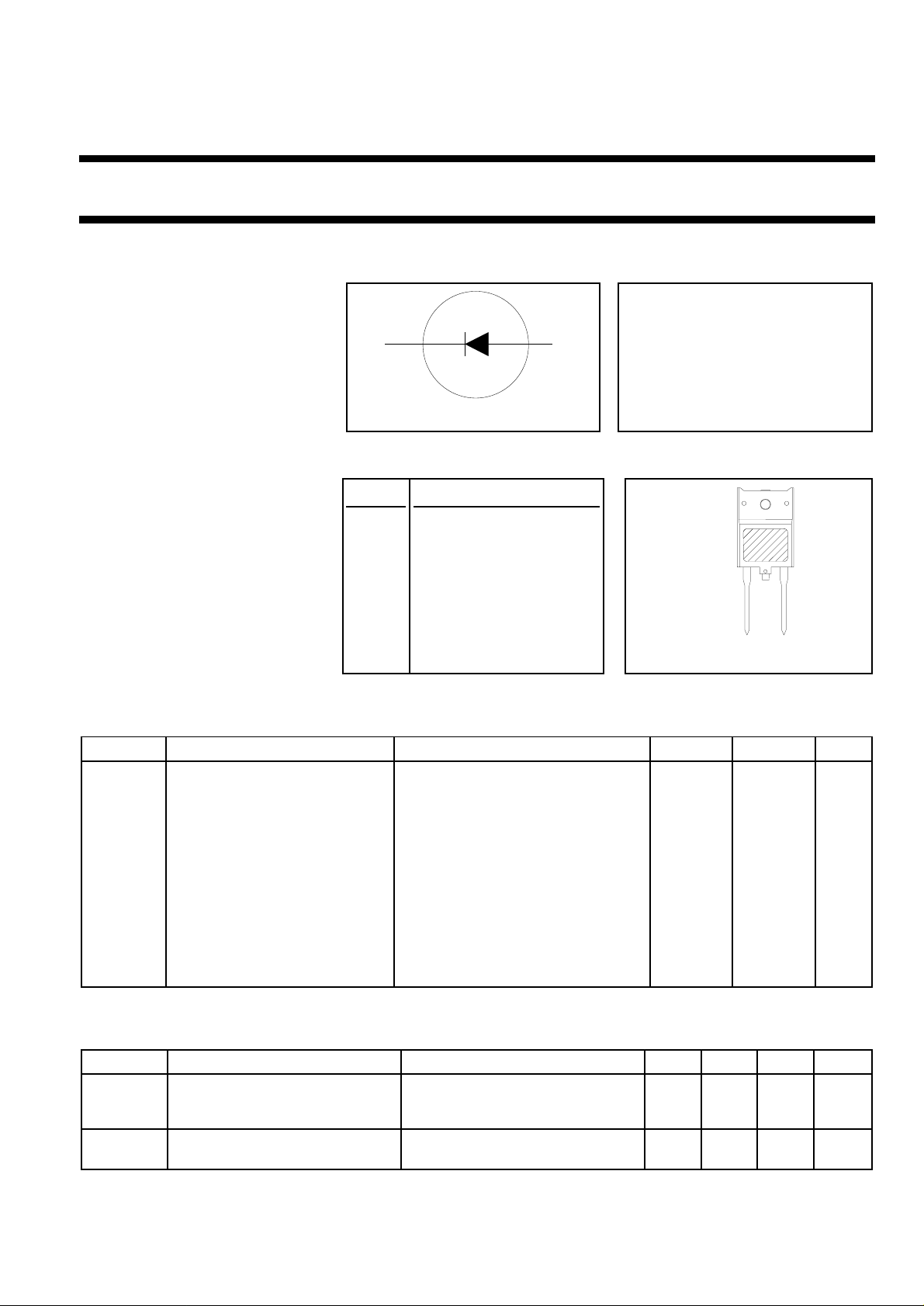
GENERAL DESCRIPTION PINNING SOD117
k a
12
= 10 A
F(AV)
I
≤ 60 A
FSM
trr ≤ 600 ns
Glass-passivated double diffused PIN DESCRIPTION
case
rectifierdiode featuring low forward
voltage drop, fast reverse recovery 1 cathode
and soft recovery characteristic.
Thedeviceisintendedforuse in TV 2 anode
receivers,series resonantswitched
mode power supplies and other tab isolated
high voltage circuits.
The BY359DX series is supplied in
12
the conventional leaded SOD117
package.
LIMITING VALUES
Limiting values in accordance with the Absolute Maximum System (IEC 134).
SYMBOL PARAMETER CONDITIONS MIN. MAX. UNIT
V
RSM
V
RRM
V
RWM
I
F(AV)
I
F(RMS)
I
FRM
I
FSM
I2tI
T
stg
T
j
Peak non-repetitive reverse - 1500 V
voltage
Peak repetitive reverse voltage - 1500 V
Crest working reverse voltage - 1300 V
Average forward current sinusoidal; a = 1.57; Ths = tbf - 10 A
RMS forward current - 20 A
Peak repetitive forward current sinusoidal; a = 1.57 - 60 A
Peak non-repetitive forward t = 10 ms - 60 A
current t = 8.3 ms - 66 A
half sine wave; Tj = 150 ˚C prior to
2
t for fusing t = 10 ms - 18 A2s
surge; with reapplied V
RWM(max)
Storage temperature -40 150 ˚C
Operating junction temperature - 150 ˚C
ISOLATION LIMITING VALUE & CHARACTERISTIC
Ths = 25 ˚C unless otherwise specified
SYMBOL PARAMETER CONDITIONS MIN. TYP. MAX. UNIT
V
isol
C
isol
April 1998 1 Rev 1.000
R.M.S. isolation voltage from f = 50-60 Hz; sinusoidal - 2500 V
both terminals to external waveform;
heatsink R.H. ≤ 65% ; clean and dustfree
Capacitance from both terminals f = 1 MHz - 10 - pF
to external heatsink

Philips Semiconductors Objective specification
Rectifier diode BY359DX-1500
fast, high-voltage
THERMAL RESISTANCES
SYMBOL PARAMETER CONDITIONS MIN. TYP. MAX. UNIT
R
th j-hs
R
th j-a
STATIC CHARACTERISTICS
Tj = 25 ˚C unless otherwise stated
SYMBOL PARAMETER CONDITIONS MIN. TYP. MAX. UNIT
V
F
I
R
DYNAMIC CHARACTERISTICS
Tj = 25 ˚C unless otherwise stated
SYMBOL PARAMETER CONDITIONS MIN. TYP. MAX. UNIT
t
rr
Q
s
V
fr
Thermal resistance junction to with heatsink compound - - tbf K/W
heatsink without heatsink compound - - tbf K/W
Thermal resistance junction to in free air. - tbf - K/W
ambient
Forward voltage IF = 20 A - 1.3 1.8 V
IF = 10 A; Tj = 150˚C - 1.00 1.5 V
Reverse current VR = 1300 V - 10 100 µA
VR = 1300 V; Tj = 100 ˚C - 50 300 µA
Reverse recovery time IF = 2 A; VR ≥ 30 V; -dIF/dt = 20 A/µs - 0.47 0.6 µs
Reverse recovery charge IF = 2 A; VR ≥ 30 V; -dIF/dt = 20 A/µs - 1.6 2.0 µC
Peak forward recovery voltage IF = 10 A; dIF/dt = 30 A/µs - 11.0 - V
April 1998 2 Rev 1.000

Philips Semiconductors Objective specification
Rectifier diode BY359DX-1500
fast, high-voltage
MECHANICAL DATA
Dimensions in mm
Net Mass: 5.9 g
4.5
16.0 max
10.0
0.7
3.3
5.8 max
3.0
27
max
22.5
max
18.1
min
10.9
Fig.1. SOD117; The seating plane is electrically isolated from all terminals.
Notes
1. Refer to mounting instructions for F-pack envelopes.
2. Epoxy meets UL94 V0 at 1/8".
25
25.1
25.7
5.1
2.2 max
1.1
0.4 M
2
0.9 max
3.3
April 1998 3 Rev 1.000

Philips Semiconductors Objective specification
Rectifier diode BY359DX-1500
fast, high-voltage
DEFINITIONS
Data sheet status
Objective specification This data sheet contains target or goal specifications for product development.
Preliminary specification This data sheet contains preliminary data; supplementary data may be published later.
Product specification This data sheet contains final product specifications.
Limiting values
Limiting values are given in accordance with the Absolute Maximum Rating System (IEC 134). Stress above one
or more of the limiting values may cause permanent damage to the device. These are stress ratings only and
operation of the device at these or at any other conditions above those given in the Characteristics sections of
this specification is not implied. Exposure to limiting values for extended periods may affect device reliability.
Application information
Where application information is given, it is advisory and does not form part of the specification.
Philips Electronics N.V. 1998
All rights are reserved. Reproduction in whole or in part is prohibited without the prior written consent of the
copyright owner.
The information presented in this document does not form part of any quotation or contract, it is believed to be
accurate and reliable and may be changed without notice. No liability will be accepted by the publisher for any
consequence of its use. Publication thereof does not convey nor imply any license under patent or other
industrial or intellectual property rights.
LIFE SUPPORT APPLICATIONS
These products are not designed for use in life support appliances, devices or systems where malfunction of these
products can be reasonably expected to result in personal injury. Philips customers using or selling these products
for use in such applications do so at their own risk and agree to fully indemnify Philips for any damages resulting
from such improper use or sale.
April 1998 4 Rev 1.000
 Loading...