

Page 1
BUZ80A
N - CHANNEL 800V - 2.5Ω - 3.8A - TO-220
FAST POWER MOS TRANSISTOR
TYPE V
DSS
R
DS(on)
I
D
BUZ 8 0A 800 V < 3 Ω 3.8 A
■ TYPICALR
■ ± 30V GATE TO SOURCE VOLTAGERATING
■ 100%AVALANCHETESTED
■ REPETITIVEAVALANCHEDATA AT 100
■ LOW INTRINSICCAPACITANCES
■ GATECHARGE MINIMIZED
■ REDUCEDTHRESHOLD VOLTAGE SPREAD
DS(on)
= 2.5
Ω
o
C
APPLICATIONS
■ HIGHCURRENT, HIGH SPEEDSWITCHING
■ SWITCHMODE POWER SUPPLIES(SMPS)
■ DC-AC CONVERTERS FOR WELDING
EQUIPMENTAND UNINTERRUPTIBLE
POWERSUPPLIESAND MOTORDRIVE
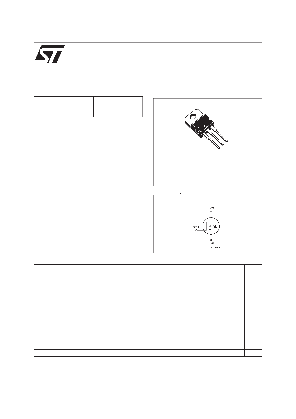
3
2
1
TO-220
INTERNAL SCHEMATIC DIAGRAM
ABSOLUTE MAXIMUM RATINGS
Symbol Parameter Value Unit
BUZ80A
V
V
V
I
DM
P
V
T
(•) Pulse width limited by safeoperating area
November 1998
Drain-source Voltage (VGS=0) 800 V
DS
Dra in- gate Voltage (RGS=20kΩ)
DGR
Gate -sourc e Voltage ± 20 V
GS
Drain Current (co ntinuous) a t Tc=25oC3.8A
I
D
I
Drain Current (co ntinuous) a t Tc=100oC2.3A
D
800 V
(•) Drain Current (pulsed) 15 A
Total Dissipation at Tc=25oC100W
tot
Derating Factor 0.8 W/
Insulat ion W ithstan d Voltage (DC) V
ISO
St orage Tem pe r ature -65 to 150
stg
Max. O perating Junc t ion Temperat u r e 150
T
j
o
C
o
C
o
C
1/9
Page 2
BUZ80A
THERMAL DATA
TO-220
R
thj-case
R
thj-amb
R
thc-sink
T
AVALANCHE CHARACTERISTICS
Symbol Para meter Max V alue Uni t
I
AR
E
Ther mal Resist ance Junction- case Max 1.25
Ther mal Resist ance Junction- ambient Max
Thermal Resistance Case-sink Typ
Maximum Lead Tem perature For S oldering Pur p os e
l
Avalanche Cu r rent, Repetitive or No t- Re petitive
(pulse width l imited by T
Single Pu lse Avalanche Energy
AS
(starting T
=25oC, ID=IAR,VDD=50V)
j
max)
j
62.5
0.5
300
3.8 A
200 mJ
o
C/W
o
C/W
o
C/W
o
C
ELECTRICAL CHARACTERISTICS
=25oC unless otherwisespecified)
(T
case
OFF
Symbol Parameter Test Conditions Min. Typ. Max. Unit
V
(BR)DSS
Drain-source
=250µAVGS=0
I
D
800 V
Break d own Vo lt age
I
DSS
I
GSS
Zero Gate Voltage
Drain Curr ent (V
GS
Gat e- b ody Leaka ge
Current (V
DS
=0)
=0)
V
=MaxRating
DS
=MaxRatingx0.8 Tc=100oC
V
DS
=± 20 V
V
GS
250
1000
± 100 nA
ON(∗)
Symbol Parameter Test Conditions Min. Typ. Max. Unit
V
GS(th)
Gate Threshold
V
DS=VGSID
= 250µA
234V
Voltage
R
DS(on)
I
D(on)
Static Drain-source On
Resistance
VGS=10V ID=1.7A
= 10V ID=1.7A Tc=100oC
V
GS
On St ate Drain Cu rr ent VDS>I
D(on)xRDS(on )max
3.8 A
2.5 3
6
VGS=10V
DYNAMIC
Symbol Parameter Test Conditions Min. Typ. Max. Unit
g
(∗)Forward
fs
Tr ansconductance
C
C
C
Input Capacitance
iss
Out put Capacitance
oss
Reverse T ransf er
rss
Capacitance
VDS>I
D(on)xRDS(on )max
ID=1.7A 1 S
VDS=25V f=1MHz VGS= 0 1100
150
35
µ
µA
Ω
Ω
pF
pF
pF
A
2/9
Page 3
BUZ80A
ELECTRICAL CHARACTERISTICS
(continued)
SWITCHINGON
Symbol Parameter Test Conditions Min. Typ. Max. Unit
t
d(on)
Turn-on Time
t
r
Rise T ime
VDD=30V ID=2.3A
=50 Ω VGS=10V
R
G
65
15090200
(see t est circuit, fi gure 3)
(di/dt)
Tur n-on Current Slope VDD= 600 V ID=3.8A
on
=50 Ω VGS=10V
R
G
80 110 A/ µ s
(see t est circuit, figure 5)
Q
Q
Q
Total Gate Charge
g
Gat e- Source Charge
gs
Gate-Drain Charge
gd
VDD= 400 V ID=5A VGS=10V 55
8
26
70 nC
SWITCHINGOFF
Symbol Parameter Test Conditions Min. Typ. Max. Unit
t
r(Voff)
t
t
Off -voltage R ise Time
Fall Time
f
Cross-over Tim e
c
VDD= 600 V ID=3.8A
=50 Ω VGS=10V
R
G
(see t est circuit, fi gure 5)
110
140
150
145
190
200
SOURCEDRAINDIODE
Symbol Parameter Test Conditions Min. Typ. Max. Unit
I
SD
I
SDM
V
SD
t
Q
I
RRM
(∗) Pulsed: Pulse duration = 300 µs, duty cycle 1.5 %
(•) Pulse width limited by safe operating area
Source-drain Current
(•)
Source-drain Current
3.8
15
(pulsed)
(∗) For ward On Voltage ISD=4A VGS=0 2 V
Reverse Recovery
rr
Time
Reverse Recovery
rr
= 4 A d i/ dt = 100 A/µs
I
SD
= 100 V Tj=150oC
V
DD
(see t est circuit, fi gure 5)
500
4.3
Charge
Reverse Recovery
17
Current
ns
ns
nC
nC
ns
ns
ns
A
A
ns
µC
A
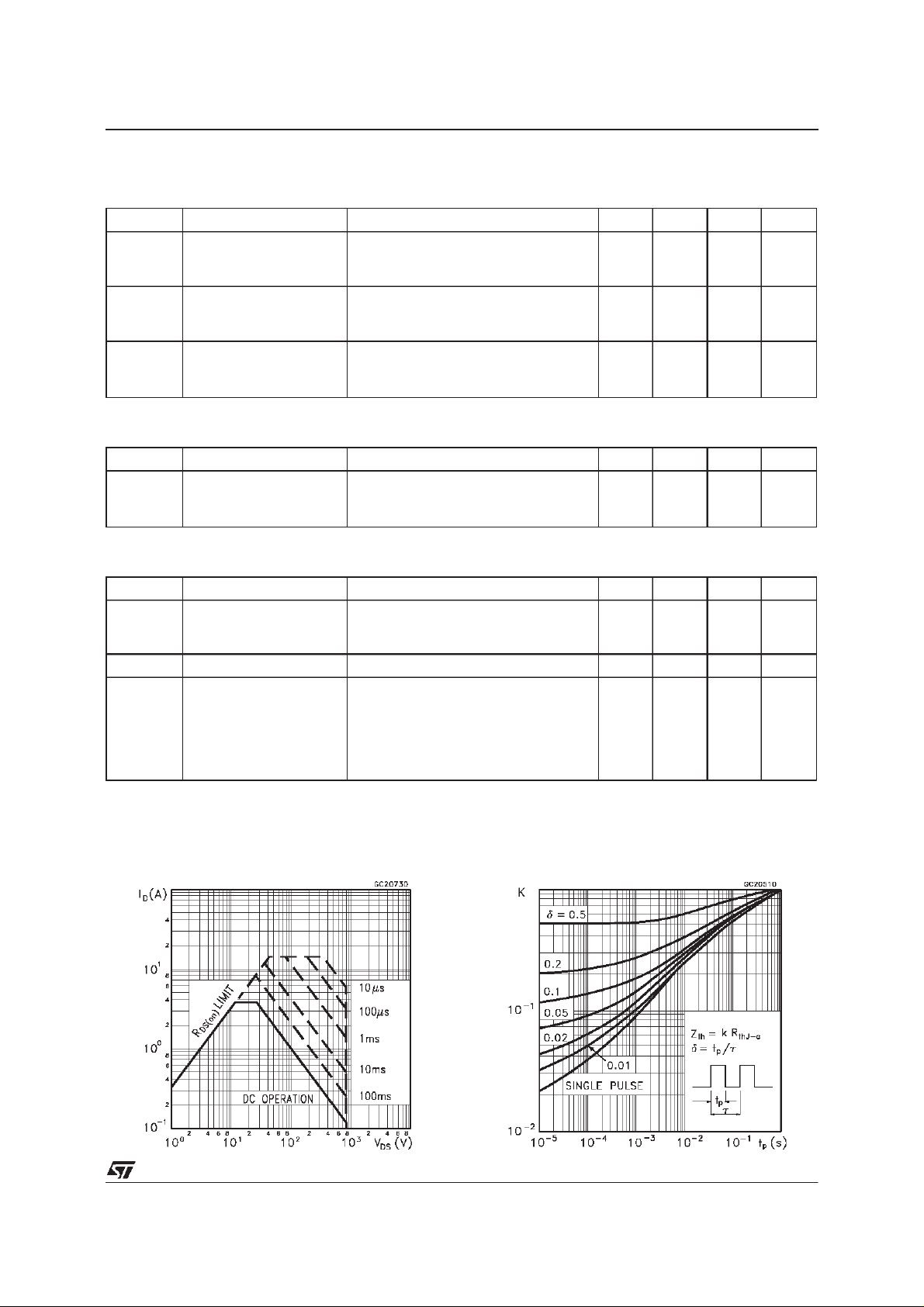
SafeOperating Area ThermalImpedance
3/9
Page 4

BUZ80A
DeratingCurve
TransferCharacteristics
OutputCharacteristics
Transconductance
Static Drain-sourceOn Resistance
4/9
Gate Charge vs Gate-sourceVoltage
Page 5

BUZ80A
CapacitanceVariations
Normalized On Resistance vs Temperature
Normalized Gate ThresholdVoltagevs
Temperature
Turn-onCurrent Slope
Turn-offDrain-source VoltageSlope
Cross-overTime
5/9
Page 6

BUZ80A
SwitchingSafe Operating Area
Source-drainDiode ForwardCharacteristics
AccidentalOverload Area
6/9
Page 7

BUZ80A
Fig. 1:
UnclampedInductive Load Test Circuit
Fig. 3: SwitchingTimes TestCircuitsFor
ResistiveLoad
Fig. 2:
UnclampedInductiveWaveform
Fig. 4: Gate Chargetest Circuit
Fig. 5:
Test Circuit For InductiveLoad Switching
And Diode Recovery Times
7/9
Page 8

BUZ80A
TO-220 MECHANICAL DATA
DIM.
mm inch
MIN. TYP. MAX. MIN. TYP. MAX.
A 4.40 4.60 0.173 0.181
C 1.23 1.32 0.048 0.051
D 2.40 2.72 0.094 0.107
D1 1.27 0.050
E 0.49 0.70 0.019 0.027
F 0.61 0.88 0.024 0.034
F1 1.14 1.70 0.044 0.067
F2 1.14 1.70 0.044 0.067
G 4.95 5.15 0.194 0.203
G1 2.4 2.7 0.094 0.106
H2 10.0 10.40 0.393 0.409
L2 16.4 0.645
L4 13.0 14.0 0.511 0.551
L5 2.65 2.95 0.104 0.116
L6 15.25 15.75 0.600 0.620
L7 6.2 6.6 0.244 0.260
L9 3.5 3.93 0.137 0.154
DIA. 3.75 3.85 0.147 0.151
E
A
L4
D
F2
F1
G1
H2
G
F
P011C
C
D1
L2
Dia.
L5
L7
L6
L9
8/9
Page 9

BUZ80A
Information furnished is believed to be accurate and reliable. However, STMicroelectronics assumes no responsibility forthe consequences
of use of such information nor for any infringement of patents or other rights of third parties which may result from its use. No license is
granted by implicationor otherwise under any patent or patent rights of STMicroelectronics. Specification mentioned in this publication are
subject to change without notice. This publication supersedes and replaces all information previously supplied. STMicroelectronics products
are not authorized for use as critical components in life support devices or systems without express written approval of STMicroelectronics.
The ST logo is a registered trademark of STMicroelectronics
1998 STMicroelectronics – Printed in Italy –All Rights Reserved
STMicroelectronics GROUP OF COMPANIES
Australia - Brazil - Canada -China -France - Germany - Italy - Japan - Korea - Malaysia -Malta - Mexico -Morocco - The Netherlands -
Singapore - Spain - Sweden - Switzerland - Taiwan - Thailand - UnitedKingdom - U.S.A.
http://www.st.com
.
9/9
 Loading...