

Page 1
HIGH POWER NPN SILICON TRANSISTORS
■ SGS-THOMS O N PREF ERRE D SA LES TYP E S
■ NPN TRANSISTOR
■ HIGH VOLTAGE CAPABILITY
■ HIGH CURRENT CAPABILITY
■ FAST SWITCHING SPEED
APPLICATIONS
■ HIGH FREQUE N CY AND EF FICE N CY
CONVERTERS
■ LINEAR AND SWITCHING INDUSTRIAL
EQUIPMENT
BUX98
BUX98A
1
2
DESCRIPTION
The BUX98 and BUX98A are silicon multiepitaxial
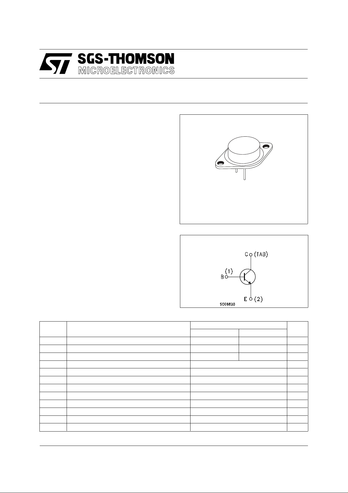
TO-3
(version R)
mesa NPN transistor in jedec TO-3 metal case,
intended and industrial applications from single
and three-phase mains operation.
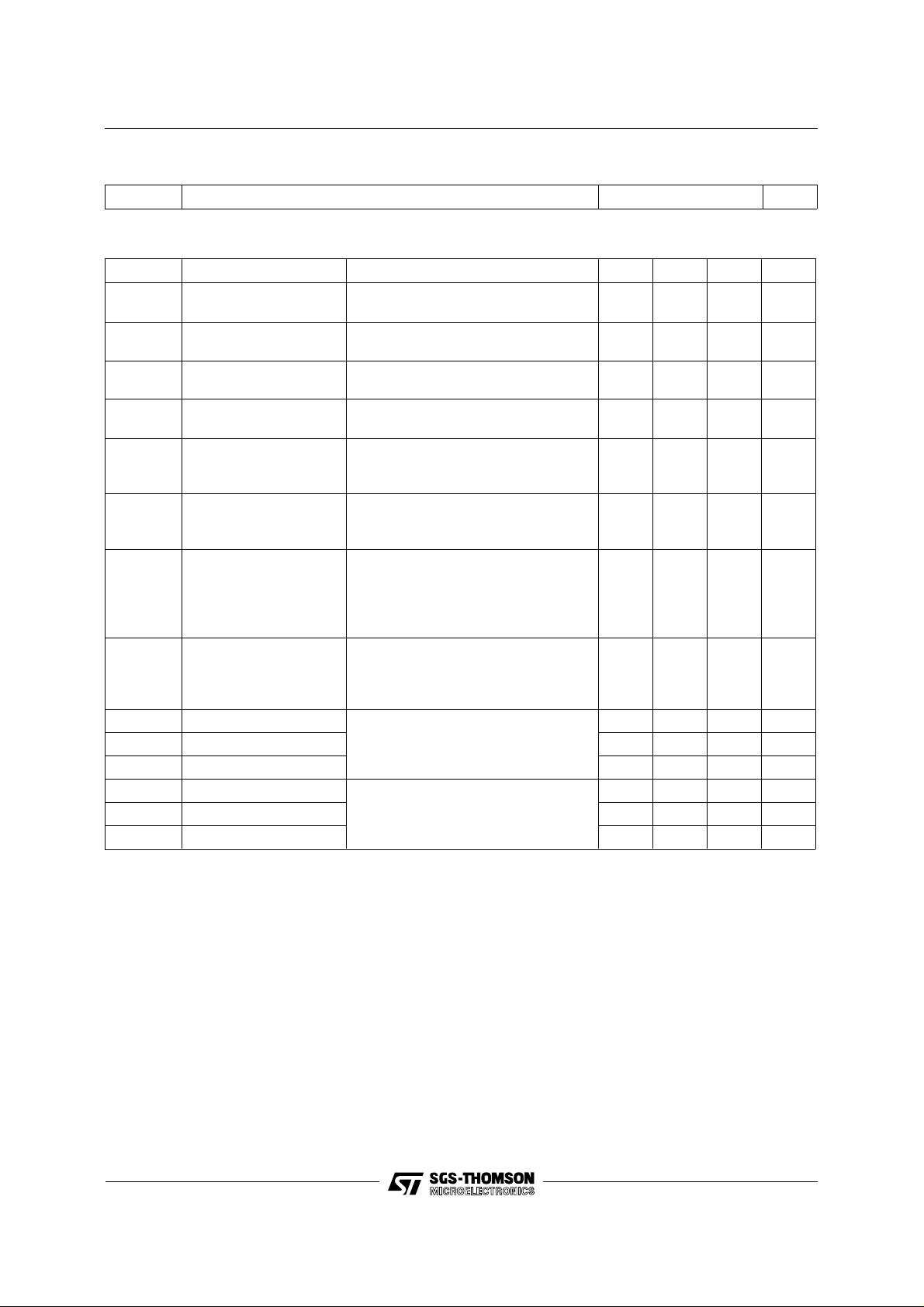
INTERNAL SCHEMATIC DIAGRAM
ABSOLUT E MAXIMUM RATI NG S
Symbol Parameter Value Unit
BUX98 BUX98A
V
V
V
V
I
I
I
P
T
Collector-Emitter Voltage (RBE = ≤ 10 Ω ) 850 1000 V
CER
Collector-Base Voltage (VBE = 0) 850 1000 V
CES
Collector-Emitter Voltage (IB = 0) 400 450 V
CEO
Emitter-Base Voltage (IC = 0) 7 V
EBO
Collector Current 30 A
I
C
Collector Peak Current (tp < 5 ms) 60 A
CM
Collector Peak Current non Rep. (tp < 20 µs) 80 A
CP
Base Current 8 A
I
B
Base Peak Current (tp < 5 ms) 30 A
BM
Total Power Dissipation at T
tot
Storage Temperature -65 to 200
stg
Max Operating Junction Temperature 200
T
j
< 25 oC 250 W
case
o
C
o
C
July 1997
1/4
Page 2
BUX98 / BUX98A
THERMAL DATA
R
thj-case
Thermal Resistance Junction-case Max 0.7
o
C/W
ELECTRICAL CHARACTERISTICS (T
= 25 oC unless otherwise specified)
case
Symbol Parameter Test Conditions Min. Typ. Max. Unit
I
CER
I
CES
I
CEO
I
EBO
V
CEO(sus)
V
CER(sus)
V
CE(sat)
Collector Cut-off
Current (R
= 10 Ω)
BE
Collector Cut-off
Current (V
BE
= 0 )
Collector Cut-off
Current (I
= 0)
B
Emitter Cut-off Current
(I
= 0)
C
∗ Collector-Emitter
Sustaining Voltage
∗ Collector-Emitter
Sustaining Voltage
∗ Collector-Emitter
Saturation Voltage
= V
V
CE
VCE = V
V
VCE = V
V
V
CES
T
CES
= V
CE
CES
T
CES
= V
CE
CEO
= 5 V 2 mA
EB
CASE
CASE
= 125 oC
= 125 oC
1
8
400
4
2mA
IC = 200 mA
for BUX98
for BUX98A
400
450
L = 2mH IC = 1 A
for BUX98
for BUX98A
850
1000
for BUX98
I
= 20 A IB = 4 A
C
1.5
for BUX98A
1.5
5
1.6
V
BE(sat)
∗ Base-Emitter
Saturation Voltage
I
= 16 A IB = 3.2 A
C
I
= 24 A IB = 5 A
C
for BUX98
I
= 20 A IB = 4 A
C
for BUX98A
I
= 16 A IB = 3.2 A
C
t
t
t
t
∗ Pulsed: Pulse duration = 300 µs, duty cycle = 1.5 %
Turn-on Time for BUX98 1 µs
on
Storage Time VCC = 150 V IC = 20 A 3 µs
s
t
Fall Time IB1 = - IB2 = 4 A 0.8 µs
f
Turn-on Time for BUX98A 1 µs
on
Storage Time VCC = 150 V IC = 16 A 3 µs
s
t
Fall Time IB1 = - IB2 = 3.2 A 0.8 µs
f
1.6
µA
mA
µA
mA
V
V
V
V
V
V
V
V
V
2/4
Page 3

P003N
TO-3 (version R) MECHANICAL DATA
BUX98 / BUX98A
DIM.
MIN. TYP. MAX. MIN. TYP. MAX.
A 11.7 0.460
B 0.96 1.10 0.037 0.043
C 1.70 0.066
D 8.7 0.342
E 20.0 0.787
G 10.9 0.429
N 16.9 0.665
P 26.2 1.031
R 3.88 4.09 0.152 0.161
U 39.50 1.555
V 30.10 1.185
mm inch
P
A
G
U
V
N
O
B
D
C
E
R
3/4
Page 4

BUX98 / BUX98A
Information furnished is believed to be accurate and reliable. However, SGS-THOMSON Microelectronics assumes no responsability for the
consequences of use of such information nor for any infringement of patents or other rights of third parties which may results from its use. No
license is granted by implication or ot h erwise under any patent or patent rights of SGS-THOMSON Microelectronics. Specifi cations mentioned
in this publication are subject to change without notice. This publication sup ersedes and replaces all information previously supplied.
SGS-THOMSON Microelectronics products are not authorized for use as critical components in life support devices or systems without express
written approval of SGS-THOMSON Microelectonics.
© 1997 SGS-THOMSON Microelectronics - Printed in Italy - All Rights Reserved
Australia - Brazil - Canada - China - France - Germany - Hong Kong - Italy - Japan - Korea - Malaysia - Malta - Morocco - The Netherlands -
Singapore - Spain - Sweden - Switzerland - Taiwan - Thailand - United Kingdom - U.S.A
SGS-THOMSON Microelectronics GROUP OF COMPANIES
. . .
4/4
 Loading...