

Page 1
HIGH POWER NPN SILICON TRANSISTORS
■ SGS-THOMS O N PREF ERRE D SA LES TYP E S
■ NPN TRANSISTOR
■ HIGH CURRENT CAPABILITY
■ FAST SWITCHING SPEED
■ VERY LOW SATURATION VOLTAGE AND
HIGH GAIN
APPLICATION
■ SWITCHING REGULATOR S
■ MOTOR CONTROL
■ HIGH FREQU E NCY AND EF FICE N CY
CONVERTERS
DESCRIPTION
The BUW48 and BUW49 are Multiepitaxial planar
NPN transistor in TO-218 pl astic package.
It’s intented for use in high frequency and
efficiency converters such us motor controllers
and industrial equipment.
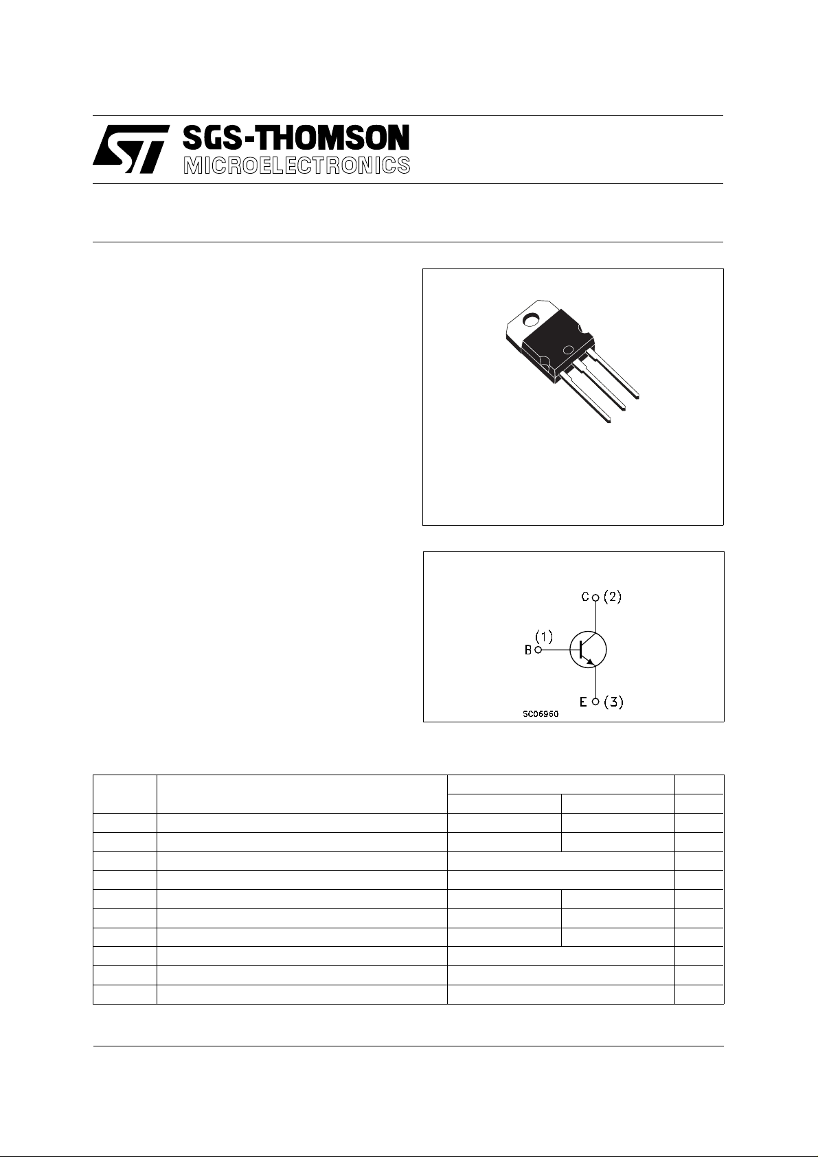
BUW48
BUW49
3
2
1
TO-218
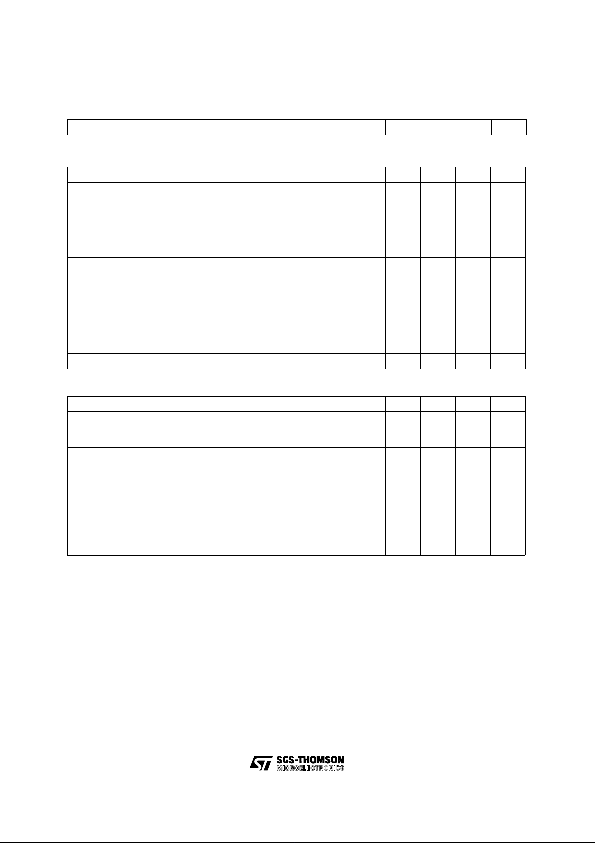
INTERNAL SCHEMATIC DIAGRAM
ABSOLUT E MAXIMUM RATI NG S
Symbol Parameter Value Unit
BUW48 BUW49 Unit
V
V
V
I
I
P
T
July 1997
Collector-emitter Voltage (VBE = -1.5V) 120 160 V
CEV
Collector-emitter Voltage (IB = 0) 60 80 V
CEO
Emitter-Base Voltage (IC = 0) 7 V
EBO
I
Collector Current 30 A
C
Collector Peak Current 45 40 A
CM
I
Base Current 8 6 A
B
Base Peak Current 12 10 A
BM
Total Power Dissipation at T
tot
Storage Temperature -65 to 175
stg
T
Max Operating Junction Temperature 175
j
< 25 oC 150 W
case
o
C
o
C
1/4
Page 2
BUW48 / BUW49
THERMAL DATA
R
thj-case
Thermal Resistance Junction-case Max 1
o
C/W
ELECTRICAL CHARACTERISTICS (T
= 25 oC unless otherwise specified)
case
Symbol Parameter Test Conditions Min. Typ. Max. Unit
I
CEX
I
EBO
V
CEO(sus)
V
V
CE(sat)
V
BE(sat)
EB0
f
Collector Cut-off
Current
Emitter Cut-off
Current (I
= 0)
C
∗ Collector-Emitter
Sustaining Voltage
Emitter-base
Voltage (I
= 0)
c
∗ Collector-Emitter
Saturation Voltage
∗ Base-Emitter
Saturation Voltage
Transition Frequency IC = 1A V
T
VCE = V
V
V
CEX VBE
= V
CE
CEX VBE
= 5 V 1 mA
EB
= -1.5V
= -1.5V Tc =125oC
1
3
IC = 0.2A L = 25 mH for BUW48
for BUW496080
= 50 mA 7 V
I
E
IC = 20A IB = 2A for BUW48
I
= 40A IB = 4A for BUW49
C
I
= 15A IB = 1.5A for BUW48
C
I
= 30A IB = 3A for BUW49
C
IC = 40A IB = 4A for BUW48
I
= 30A IB = 3A for BUW49
C
= 15V f = 15 MHz 8 MHz
CE
0.6
1.4
0.5
1.2
2.1
2
RESISTIVE LOAD
Symbol Parameter Test Conditions Min. Typ. Max. Unit
t
t
t
t
t
t
∗ Pulsed: Pulse duration = 300 µs, duty cycle < 1.5 %
on
s
t
f
s
t
f
on
s
t
f
s
t
f
Turn-on Time
Storage Time
Fall Time
Storage Time
Fall Time
Turn-on Time
Storage Time
Fall Time
Storage Time
Fall Time
for BUW48
V
CC
I
B1
for BUW48
V
CC
I
B1
for BUW49
V
CC
I
B1
for BUW49
V
CC
I
B1
= 60V IC = 40A
= -I
= 4A
B2
= 60V IC = 40A
= -I
= 4A
B2
= 80V IC = 30A
= -I
= 4A
B2
= 80V IC = 30A
= -I
= 4A
B2
1.2
0.6
0.17
0.8
0.6
0.15
1.5
1.1
0.25
1.65
0.5
1.2
1.1
0.25
1.65
0.5
mA
mA
V
V
V
V
V
V
V
V
µs
µs
µs
µs
µs
µs
µs
µs
µs
µs
2/4
Page 3

TO-218 (SOT-93) MECHANICAL DATA
BUW48 / BUW49
DIM.
MIN. TYP. MAX. MIN. TYP. MAX.
A 4.7 4.9 0.185 0.193
C 1.17 1.37 0.046 0.054
D2.5 0.098
E 0.5 0.78 0.019 0.030
F 1.1 1.3 0.043 0.051
G 10.8 11.1 0.425 0.437
H 14.7 15.2 0.578 0.598
L2 – 16.2 – 0.637
L3 18 0.708
L5 3.95 4.15 0.155 0.163
L6 31 1.220
R – 12.2 – 0.480
Ø 4 4.1 0.157 0.161
mm inch
H
A
C
L5
E
D
L6
L3
L2
G
¯
F
R
1
2 3
P025A
3/4
Page 4

BUW48 / BUW49
Information furnished is believed to be accurate and reliable. However, SGS-THOMSON Microelectronics assumes no responsability for the
consequences of use of such information nor for any infringement of patents or other rights of third parties which may results from its use. No
license is granted by implication or ot h erwise under any patent or patent rights of SGS-THOMSON Microelectronics. Specifi cations mentioned
in this publication are subject to change without notice. This publication sup ersedes and replaces all information previously supplied.
SGS-THOMSON Microelectronics products are not authorized for use as critical components in life support devices or systems without express
written approval of SGS-THOMSON Microelectonics.
© 1997 SGS-THOMSON Microelectronics - Printed in Italy - All Rights Reserved
Australia - Brazil - Canada - China - France - Germany - Hong Kong - Italy - Japan - Korea - Malaysia - Malta - Morocco - The Netherlands -
Singapore - Spain - Sweden - Switzerland - Taiwan - Thailand - United Kingdom - U.S.A
SGS-THOMSON Microelectronics GROUP OF COMPANIES
. . .
4/4
 Loading...