

Page 1
®
HIGH VOLTAGE FAST-SWITCHING
■
STMicroelectronics PREFERRED
SALESTYPE
■
HIGH VOLTAGE CA PA BILIT Y (> 1500 V)
■
VERY HIGH SWITCHING SPEED
APPLICATIONS:
■
HORIZONTAL DEFLECTION FOR HIGH-END
COLOUR TV AND 19" MONITORS
DESCRIPTION
The BUW1015 is manufactured using
Multiepitaxial Mesa technology for cost-effective
high performance and uses a Hollow Emitter
structure to enhance switching speeds.
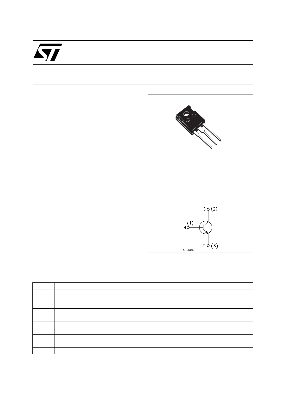
BUW1015
NPN POWER TRANSISTOR
3
2
1
TO-247
INTERNAL SCHEMATIC DIAGRA M
ABSOLUTE MAXIMUM RATINGS
Symbol Parameter Value Unit
V
V
V
I
I
P
T
Collector-Base Voltage (IE = 0) 1500 V
CBO
Collector-Emitter Voltage (IB = 0) 700 V
CEO
Emitter-Base Voltage (IC = 0) 10 V
EBO
Collector Current 14 A
I
C
Collector Peak Current (tp < 5 ms) 18 A
CM
Base Current 8 A
I
B
Base Peak Current (tp < 5 ms) 11 A
BM
Total Dissipation at Tc = 25 oC 160 W
tot
Storage Temperature -65 to 150
stg
Max. Operating Junction Temperature 150
T
j
o
C
o
C
February 2002
1/7
Page 2
BUW1015
THERMAL DATA
R
thj-case
Thermal Resistance Junction-case Max 0.78
o
C/W
ELECTRICAL CHARACT ER ISTI CS
= 25 oC unless otherwise specified)
(T
case
Symbol Parameter Test Conditions Min. Typ. Max. Unit
I
CES
I
EBO
V
CEO(sus)
Collector Cut-off
Current (V
BE
= 0)
Emitter Cut-off Current
(I
= 0)
C
∗ Collector-Emitter
= 1500 V
V
CE
V
= 1500 V Tj = 125 oC
CE
= 5 V 100 µA
V
EB
I
= 100 mA 700 V
C
0.2
2
Sustaining Voltage
(I
= 0)
B
V
EBO
Emitter-Base Voltage
(I
V
∗ Collector-Emitter
CE(sat)
= 0)
C
= 10 mA 10 V
I
E
= 10 A IB = 2 A 1.5 V
I
C
Saturation Voltage
V
∗ Base-Emitter
BE(sat)
= 10 A IB = 2 A 1.5 V
I
C
Saturation Voltage
h
∗ DC Current Gain I
FE
RESISTIVE LOAD
s
t
f
Storage Time
Fall Time
t
INDUCTIVE LOAD
t
s
t
f
Storage Time
Fall Time
INDUCTIVE LOAD
s
t
f
Storage Time
Fall Time
t
∗
Pulsed: Pulse duration = 300 µs, duty cycle 1.5 %
= 10 A VCE = 5 V
C
I
= 10 A VCE = 5 V Tj = 100 oC
C
V
= 400 V IC = 10 A
CC
I
= 2 A IB2= -6 A 1.5
B1
I
= 10 A f = 31250 Hz
C
I
= 2 A I
B1
V
I
C
I
B1
V
V
= 1200 sin
ceflyback
= 6 A f = 64 KHz
= 1 A
= - 2 V
beoff
= 1100 sin
ceflyback
B2
= -6 A
π
10
5
π
10
5
6
6
t V
t V
7
5
10 14
110
4
220
3.7
200
mA
mA
µs
ns
µs
ns
µs
ns
2/7
Page 3
BUW1015
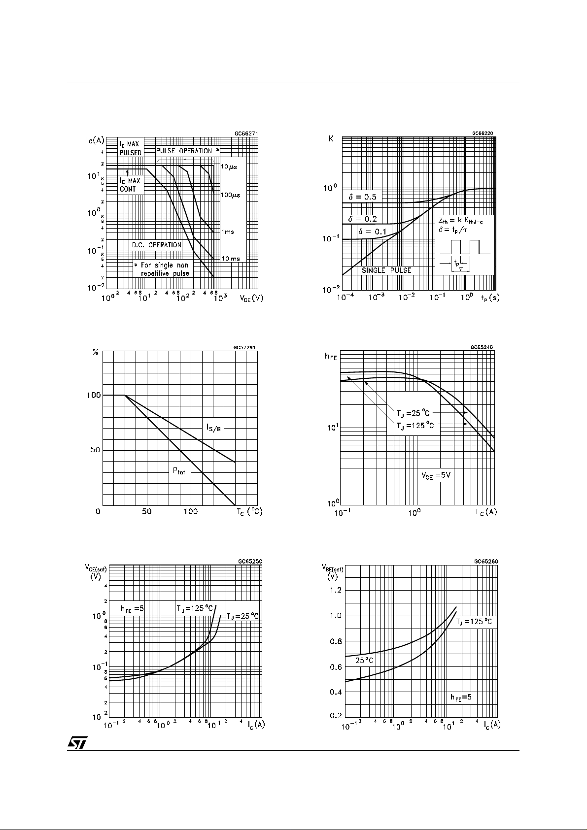
Safe Operating Area
Derating Curve
Thermal Impedance
DC Current Gain
Collector Emitter Saturation Voltage
Base Emitter Saturation Voltage
3/7
Page 4

BUW1015
Power Losses at 64 KHz Switching Time Inductive Load at 64KHz
(see figure 2)
Reverse Biased SOA
BASE DRIVE INFORMATION
In order to saturate the power switch and reduce
conduction losses, adequate direct base current
I
has to be provided for the lowest gain hFE at T
B1
= 100 oC (line scan phase). On the other hand,
negative base current I
must be provided the
B2
transistor to turn off (retrace phase). Most of the
dissipation, especially in the deflection
application, occurs at switch-off so it is essential
to determine the value of I
power losses, fall time t
and, consequently, Tj. A
f
which minimizes
B2
new set of curves have been defined to give total
power losses, t
and tf as a function of IB1 at 64
s
KHz scanning frequencies for choosing the
4/7
optimum drive. The test circuit is illustrated in
figure 1.
j
The values of L and C are calculated from the
following equations:
1
L
2
ω =
(
2
1
2
)
I
=
C
π
f
=
C
2
1
L
√
(
C
V
CEfly
2
)
Where IC= operating collector current, V
flyback voltage, f= frequency of oscillation during
retrace.
CEfly
=
Page 5

BUW1015
Figure 1:
Figure 2:
Inductive Load Switching Test Circuit.
Switching Waveforms in a Deflection Circuit
5/7
Page 6

BUW1015
TO-247 MECHANICAL DATA
DIM.
MIN. TYP. MAX. MIN. TYP. MAX.
A 4.7 5.3 0.185 0.209
D 2.2 2.6 0.087 0.102
E 0.4 0.8 0.016 0.031
F 1 1.4 0.039 0.055
F3 2 2.4 0.079 0.094
F4 3 3.4 0.118 0.134
G 10.9 0.429
H 15.3 15.9 0.602 0.626
L 19.7 20.3 0.776 0.779
L3 14.2 14.8 0.559 0.582
L4 34.6 1.362
L5 5.5 0.217
M 2 3 0.079 0.118
mm inch
6/7
P025P
Page 7

BUW1015
Information furnished is believed to be accurate and reliable. However, STMicroelectronics assumes no responsibility for the consequences
of use of such inform ation nor for any in fringe ment o f patents or other rig hts of third par ties wh ich may result from its u se. N o li cen se is
granted by implication or otherwise under any patent or patent rights of STMicroelectronics. Specification mentioned in this publication are
subject to change without notice. This publication supersedes and replaces all information previously supplied. STMicroelectronics products
are not authorized f or use as critical components in life support devices or systems without express written approval of STMicroelectronics.
The ST logo is a trademark of STMicroelectronics
© 2002 STMicroelectro nics – Printed in Italy – All Rights Reserved
STMicroelectronics GROUP OF COMPANIES
Australia - Brazil - Canada - China - Finland - France - Germany - Hong Kong - India - Israel - Italy - Japan - Malaysia - Malta - Morocco -
Singapore - Spain - Sweden - Switzerland - United Kingdom - United States.
http://www.st.com
7/7
 Loading...