

Page 1
1
Motorola Bipolar Power Transistor Device Data
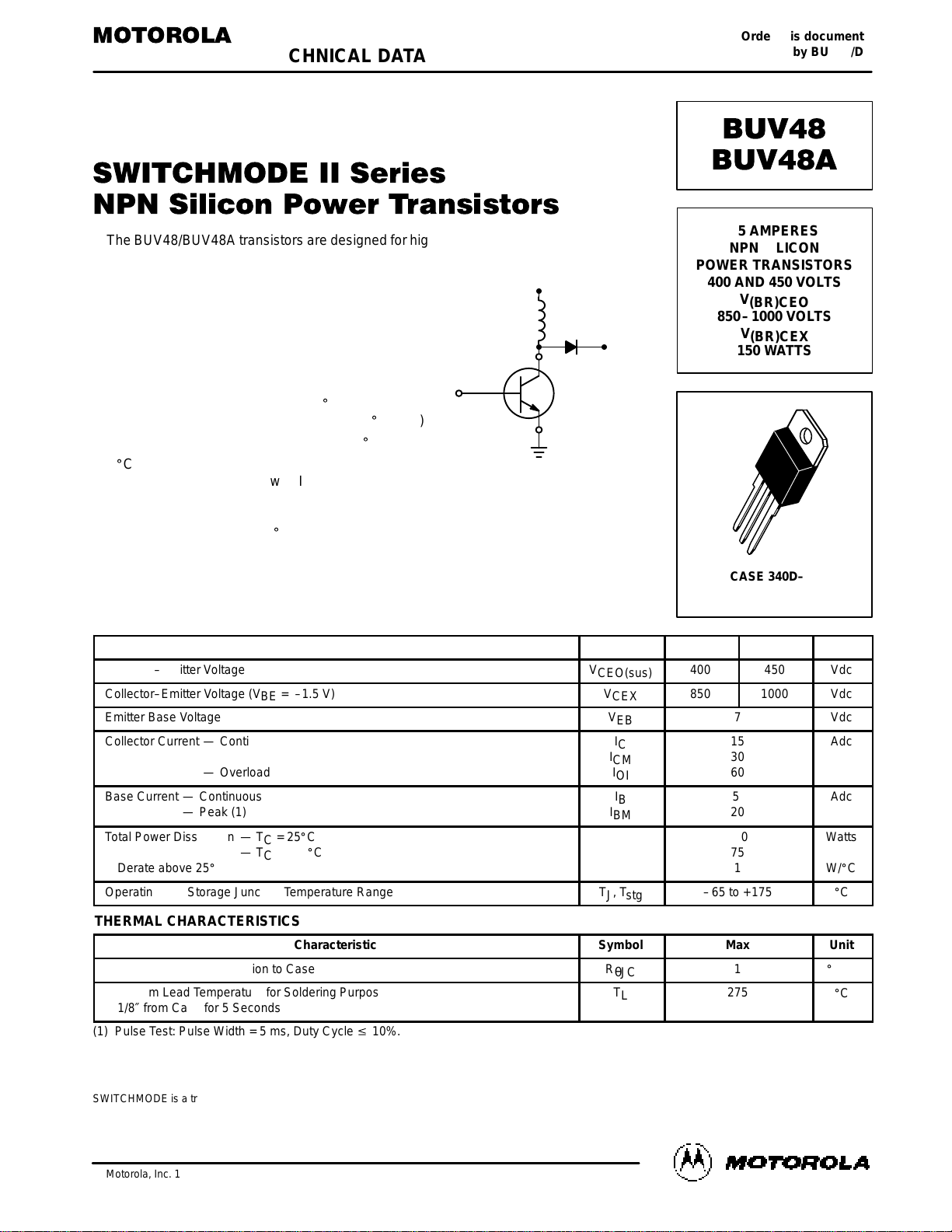
The BUV48/BUV48A transistors are designed for high–voltage, high–speed, power
switching in inductive circuits where fall time is critical. They are particularly suited for
line–operated switchmode applications such as:
• Switching Regulators
• Inverters
• Solenoid and Relay Drivers
• Motor Controls
• Deflection Circuits
Fast Turn–Off Times
60 ns Inductive Fall Time — 25_C (Typ)
120 ns Inductive Crossover Time — 25_C (Typ)
Operating Temperature Range –65 to +175_C
100_C Performance Specified for:
Reverse–Biased SOA with Inductive Loads
Switching Times with Inductive Loads
Saturation Voltage
Leakage Currents (125_C)
MAXIMUM RATINGS
Rating
Symbol
BUV48
BUV48A
ÎÎÎ
ÎÎÎ
ÎÎÎ
Unit
Collector–Emitter Voltage
V
CEO(sus)
400
450
ÎÎÎ
ÎÎÎ
ÎÎÎ
Vdc
Collector–Emitter Voltage (VBE = –1.5 V)
V
CEX
850
1000
ÎÎÎ
ÎÎÎ
ÎÎÎ
Vdc
Emitter Base Voltage
V
EB
7
ÎÎÎ
ÎÎÎ
ÎÎÎ
Vdc
Collector Current — Continuous
— Peak (1)
— Overload
I
C
I
CM
I
OI
15
30
60
ÎÎÎ
ÎÎÎ
ÎÎÎ
ÎÎÎ
Adc
Base Current — Continuous
— Peak (1)
I
B
I
BM
5
20
ÎÎÎ
ÎÎÎ
ÎÎÎ
ÎÎÎ
Adc
Total Power Dissipation — TC = 25_C
— TC = 100_C
Derate above 25_C
P
D
150
75
1
ÎÎÎ
ÎÎÎ
ÎÎÎ
ÎÎÎ
Watts
W/_C
Operating and Storage Junction Temperature Range
TJ, T
stg
–65 to +175
ÎÎÎ
ÎÎÎ
ÎÎÎ
_
C
THERMAL CHARACTERISTICS
Characteristic
Symbol
Max
ÎÎÎ
ÎÎÎ
ÎÎÎ
Unit
Thermal Resistance, Junction to Case
R
θJC
1
ÎÎÎ
ÎÎÎ
ÎÎÎ
_
C/W
Maximum Lead Temperature for Soldering Purposes:
1/8″ from Case for 5 Seconds
T
L
275
ÎÎÎ
ÎÎÎ
ÎÎÎ
_
C
(1) Pulse Test: Pulse Width = 5 ms, Duty Cycle v 10%.
SWITCHMODE is a trademark of Motorola, Inc.
SEMICONDUCTOR TECHNICAL DATA
Order this document
by BUV48/D
Motorola, Inc. 1995
15 AMPERES
NPN SILICON
POWER TRANSISTORS
400 AND 450 VOLTS
V
(BR)CEO
850–1000 VOLTS
V
(BR)CEX
150 WATTS
CASE 340D–01
TO–218 TYPE
REV 7
Page 2
2
Motorola Bipolar Power Transistor Device Data
ELECTRICAL CHARACTERISTICS (T
C
= 25_C unless otherwise noted)
Characteristic
Symbol
Min
Typ
Max
ÎÎÎ
ÎÎÎ
ÎÎÎ
Unit
OFF CHARACTERISTICS (1)
ÎÎÎ
ÎÎÎ
ÎÎÎ
(IC = 200 mA, IB = 0) L = 25 mH BUV48
BUV48A
400
450————
ÎÎÎ
ÎÎÎ
ÎÎÎ
ÎÎÎ
Collector Cutoff Current
(V
CEX
= Rated Value, V
BE(off)
= 1.5 Vdc)
(V
CEX
= Rated Value, V
BE(off)
= 1.5 Vdc, TC = 125_C)
I
CEX
—
—
—
—
0.2
2
ÎÎÎ
ÎÎÎ
ÎÎÎ
ÎÎÎ
mAdc
ÎÎÎ
ÎÎÎ
ÎÎÎ
(VCE = Rated V
CEX
, RBE = 10 Ω) TC = 25_C
TC = 125_C
————0.5
3
ÎÎÎ
ÎÎÎ
ÎÎÎ
Emitter Cutoff Current
(VEB = 5 Vdc, IC = 0)
I
EBO
—
—
0.1
ÎÎÎ
ÎÎÎ
ÎÎÎ
ÎÎÎ
mAdc
Emitter–Base Breakdown Voltage
(IE = 50 mA – IC = 0)
V
(BR)EBO
7
—
—
ÎÎÎ
ÎÎÎ
ÎÎÎ
ÎÎÎ
Vdc
SECOND BREAKDOWN
Second Breakdown Collector Current with Base Forward Biased
I
S/b
See Figure 12
ÎÎÎ
ÎÎÎ
ÎÎÎ
Clamped Inductive SOA with Base Reverse Biased
RBSOA
See Figure 13
ÎÎÎ
ÎÎÎ
ÎÎÎ
ON CHARACTERISTICS (1)
DC Current Gain
(IC = 10 Adc, VCE = 5 Vdc) BUV48
(IC = 8 Adc, VCE = 5 Vdc) BUV48A
h
FE
8
8
—
—
—
—
ÎÎÎ
ÎÎÎ
ÎÎÎ
ÎÎÎ
ÎÎÎ
Collector–Emitter Saturation Voltage
(IC = 10 Adc, IB = 2 Adc)
(IC = 15 Adc, IB = 3 Adc) BUV48
(IC = 10 Adc, IB = 2 Adc, TC = 100_C)
(IC = 8 Adc, IB = 1.6 Adc)
(IC = 12 Adc, IB = 2.4 Adc) BUV48A
(IC = 8 Adc, IB = 1.6 Adc, TC = 100_C)
V
CE(sat)
—
—
—
—
—
—
—
—
—
—
—
—
1.5
5
2
1.5
5
2
ÎÎÎ
ÎÎÎ
ÎÎÎ
ÎÎÎ
ÎÎÎ
ÎÎÎ
ÎÎÎ
Vdc
Base–Emitter Saturation Voltage
(IC = 10 Adc, IB = 2 Adc) BUV48
(IC = 10 Adc, IB = 2 Adc, TC = 100_C)
(IC = 8 Adc, IB = 1.6 Adc) BUV48A
(IC = 8 Adc, IB = 1.6 Adc, TC = 100_C)
V
BE(sat)
—
—
—
—
—
—
—
—
1.6
1.6
1.6
1.6
ÎÎÎ
ÎÎÎ
ÎÎÎ
ÎÎÎ
ÎÎÎ
Vdc
DYNAMIC CHARACTERISTICS
Output Capacitance
(VCB = 10 Vdc, IE = 0, f
test
= 1 MHz)
C
ob
—
—
350
ÎÎÎ
ÎÎÎ
ÎÎÎ
ÎÎÎ
pF
SWITCHING CHARACTERISTICS
Resistive Load (Table 1)
Delay Time
ОООООООООООООО
ОООООООООООООО
ОООООООООООООО
t
d
—
0.1
0.2
ÎÎÎ
ÎÎÎ
ÎÎÎ
µs
Rise Time
ОООООООООООООО
ОООООООООООООО
ОООООООООООООО
IC = 10 A, IB, = 2 A BUV48
IC = 8 A, IB, = 1.6 A BUV48A
t
r
—
0.4
0.7
ÎÎÎ
ÎÎÎ
ÎÎÎ
Storage Time
ОООООООООООООО
ОООООООООООООО
ОООООООООООООО
IC = 8 A, IB, = 1.6 A BUV48A
Duty Cycle v 2%, V
BE(off)
= 5 V
t
s
—
1.3
2
ÎÎÎ
ÎÎÎ
ÎÎÎ
Fall Time
ОООООООООООООО
ОООООООООООООО
ОООООООООООООО
v
2%, V
BE(off)
= 5 V
Tp = 30 µs, VCC = 300 V
t
f
—
0.2
0.4
ÎÎÎ
ÎÎÎ
ÎÎÎ
Inductive Load, Clamped (Table 1)
Storage Time
ООООООООО
ООООООООО
ООООООООО
t
sv
—
1.3
—
ÎÎÎ
ÎÎÎ
ÎÎÎ
µs
Fall Time
ООООООООО
ООООООООО
ООООООООО
IC = 10 A BUV48
I
= 2 A
(TC = 25_C)
t
fi
—
0.06
—
ÎÎÎ
ÎÎÎ
ÎÎÎ
Storage Time
ООООООООО
ООООООООО
ООООООООО
IB1 = 2 A
t
sv
—
1.5
2.5
ÎÎÎ
ÎÎÎ
ÎÎÎ
Crossover Time
ООООООООО
ООООООООО
ООООООООО
IC = 8 A BUV48A
I
= 1.6 A
_
C)
t
c
—
0.3
0.6
ÎÎÎ
ÎÎÎ
ÎÎÎ
Fall Time
ООООООООО
ООООООООО
ООООООООО
IB1 = 1.6 A
_
C)
t
fi
—
0.17
0.35
ÎÎÎ
ÎÎÎ
ÎÎÎ
(1) Pulse Test: Pulse Width = 300 µs, Duty Cycle v 2%.
Vcl = 300 V, V
BE(off)
= 5 V, Lc = 180 µH
Collector–Emitter Sustaining Voltage (Table 1)
Collector Cutoff Current
(TC = 100
V
CEO(sus)
I
CER
Vdc
mAdc
Page 3
3
Motorola Bipolar Power Transistor Device Data
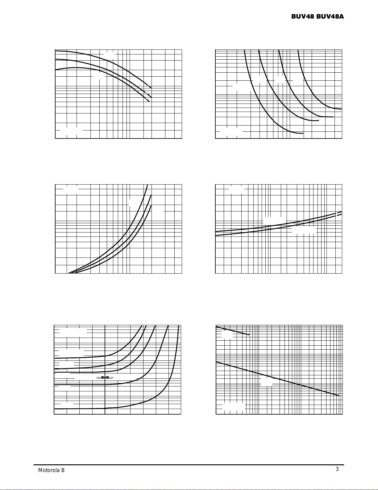
DC CHARACTERISTICS
, COLLECTOR CURRENT ( A)
µ
I
C
V
BE
, BASE–EMITTER VOLTAGE (VOLTS)
V
CE
, COLLECTOR–EMITTER VOLTAGE (VOLTS)
V
CE
, COLLECTOR–EMITTER VOLTAGE (VOLTS)
0.1
IC, COLLECTOR CURRENT (AMPS)
0.3 3
2
1
0.7
0.5
5
IC, COLLECTOR CURRENT (AMPS)
3
2
1
0.7
0.5
0.3
0.2
0.3
IC = 5 A
50
1
Figure 1. DC Current Gain
IC, COLLECTOR CURRENT (AMPS)
1
2 3 5 8 10 20 30 50
20
10
7
Figure 2. Collector Saturation Region
0.1
IB, BASE CURRENT (AMPS)
0.1
0.3 0.5
3
0.5
0.3
30
h
FE
, DC CURRENT GAIN
5
3
2
VCE = 5 V
TJ = 150°C
1 2 3 4
Figure 3. Collector–Emitter Saturation Voltage
1011 2 3 7 10 5020 305
Figure 4. Base–Emitter Voltage
Figure 5. Collector Cutoff Region
10
5
1
–0.4
Figure 6. Capacitance
VBE, BASE–EMITTER VOLTAGE (VOLTS)
10
–1
–0.2 0 0.2 0.4 0.6
10 k
1
VR, REVERSE VOLTAGE (VOLTS)
10
10
1 k
10
0
100 1000
100
FORWARD
0.1
VCE = 250 V
125°C
90%
75°C
7.5 A
TJ = 100°C
REVERSE
10
1
10
2
10
3
10
4
C
ob
β
f
= 5
25°C
10%
TC = 25°C
10 A 15 A
90%
10%
TJ = 25°C
β
f
= 5
100°C
C, CAPACITANCE (pF)
C
ib
TJ = 25°C
Page 4

4
Motorola Bipolar Power Transistor Device Data
Table 1. Test Conditions for Dynamic Performance
V
CEO(sus)
RBSOA AND INDUCTIVE SWITCHING RESISTIVE SWITCHING
INPUT
CONDITIONS
CIRCUIT
VALUES
TEST CIRCUITS
20
1
0
PW Varied to Attain
IC = 200 mA
L
coil
= 25 mH, VCC = 10 V
R
coil
= 0.7 Ω
L
coil
= 180 µH
R
coil
= 0.05 Ω
VCC = 20 V
VCC = 300 V
RL = 83 Ω
Pulse Width = 10 µs
INDUCTIVE TEST CIRCUIT
TURN–ON TIME
IB1 adjusted to
obtain the forced
hFE desired
TURN–OFF TIME
Use inductive switching
driver as the input to
the resistive test circuit.
t1 Adjusted to
Obtain I
C
Test Equipment
Scope — Tektronix
475 or Equivalent
RESISTIVE TEST CIRCUITOUTPUT WAVEFORMS
2
I
B1
1
2
V
clamp
= 300 V
RB ADJUSTED TO ATTAIN DESIRED I
B1
+10 V
220 100
680 pF
100
PULSES
δ
= 3%
33
2 W
33
2 W
160
D1
22
µ
F
D3
22
680 pF
MM3735
1N4934D1 D2 D3 D4
2N3763
160
680 pF
22
D4
0.22
µ
F
D3
2N6438
+10 V
MR854
0.1
µ
F
2N6339
MR854
Ib1 ADJUST
dTb ADJUST
dT
Ib2 ADJUST
V
CC
1
INPUT
2
R
coil
L
coil
V
CC
V
clamp
RS =
0.1
Ω
1N4937
OR
EQUIVALENT
TUT
SEE ABOVE FOR
DETAILED CONDITIONS
t
1
I
C
V
CE
I
C(pk)
tf Clamped
t
f
t
t
t
2
TIME
VCE
or
V
clamp
t1 ≈
L
coil (IC
pk
)
V
CC
t2 ≈
L
coil (IC
pk
)
V
Clamp
1
2
TUT
R
L
V
CC
t
rv
V
BE(off)
, BASE–EMITTER VOLTAGE (VOLTS)
TIME
Figure 7. Inductive Switching Measurements Figure 8. Peak–Reverse Current
1 2 3 4 5 6
10
8
6
4
2
0
, BASE CURRENT (AMPS)I
B2(pk)
0
β
f
= 5
IC = 10 A
I
C
V
CE
90% I
B1
t
sv
IC pk
V
CE(pk)
90% V
CE(pk)
90% I
C(pk)
10% V
CE(pk)
10%
IC pk
2% I
C
I
B
t
fi
t
ti
t
c
Page 5

5
Motorola Bipolar Power Transistor Device Data
SWITCHING TIMES NOTE
In resistive switching circuits, rise, fall, and storage times
have been defined and a pply to both current and voltage
waveforms since they are in phase. However, for inductive
loads which are common to SWITCHMODE power supplies
and hammer drivers, current and voltage waveforms are not
in phase. Therefore, separate measurements must be made
on each waveform to determine the total switching time. For
this reason, the following new terms have been defined.
tsv= Voltage Storage Time, 90% IB1 to 10% V
clamp
trv= Voltage Rise Time, 10–90% V
clamp
tfi= Current Fall Time, 90–10% I
C
tti= Current Tail, 10–2% I
C
tc= Crossover Time, 10% V
clamp
to 10% I
C
An enlarged portion of the inductive switching waveforms is
shown in Figure 7 to aid in the visual identity of these terms.
For the designer, there is minimal switching loss during
storage time and the predominant switching power losses
occur during the crossover interval and can be obtained using the standard equation from AN–222:
P
SWT
= 1/2 VCCIC(tc) f
In general, trv + tfi ] tc. However, at lower test currents this
relationship may not be valid.
As is common with most switching transistors, resistive
switching is specified at 25_C and has become a benchmark
for designers. However, for designers of high frequency converter circuits, the user oriented specifications which make
this a “SWITCHMODE” transistor are the inductive switching
speeds (tc and tsv) which are guaranteed at 100_C.
1
Figure 9. Storage Time, t
sv
IC, COLLECTOR CURRENT (AMPS)
2 5
0.1
Figure 10. Crossover and Fall Times
5
3
1
0.7
0.5
50
IC, COLLECTOR CURRENT (AMPS)
3 7
0
Figure 11a. Turn–Off Times versus Forced Gain
β
f
, FORCED GAIN
0.01
1 2 4 5
2
0.5
0.3
0.2
Figure 11b. Turn–Off Times versus Ib2/Ib
1
Ib2/Ib
1
3
1
0.1
3
TC = 100°C
TC = 25°C
IC = 10 A
V
BE(off)
= 5 V
0.01
1
0.5
0.2
0.3
0.1
t, TIME ( s)
µ
2
0.3
0.2
2010 30
β
f
= 5
TC = 25°C
t, TIME ( s)
µ
0.05
0.02
0.03
1 2 5 503 7 2010 30
β
f
= 5
TC = 100°C
TC = 25°C
t
c
t
fi
0.05
0.03
0.02
6 8 97 10
t
sv
t
fi
t
c
t, TIME ( s)
µ
t, TIME ( s)
µ
0.01
2
0.5
0.3
0.2
3
1
0.1
0.05
0.03
0.02
0 1 2 4 53 6 8 97 10
TC = 25°C
IC = 10 A
β
f
= 5 V
t
sv
t
fi
t
c
TC = 100°C
TC = 25°C
INDUCTIVE SWITCHING
Page 6

6
Motorola Bipolar Power Transistor Device Data
The Safe Operating Area figures shown in Figures 12 and 13 are
specified for these devices under the test conditions shown.
1
Figure 12. Forward Bias Safe Operating Area
VCE, COLLECTOR–EMITTER VOLTAGE (VOLTS)
5 50
0.01
30
10
2
1
5
0.5
100010 100
0
FIgure 13. Reverse Bias Safe Operating Area
VCE, COLLECTOR–EMITTER VOLTAGE (VOLTS)
0
200 400
40
20
50
600
TC = 25°C
TC = 100°C
IC/IB
≥
5
I
C
, COLLECTOR CURRENT (AMPS)
0.1
200
DC
1 ms
I
C
, COLLECTOR CURRENT (AMPS)
tr ≤ 0.7 µs
LIMIT ONLY
FOR TURN ON
2 20 500
30
10
0.2
0.05
0.02
800 1000
V
BE(off)
= 5 V
BUV48 BUV48A
SAFE OPERATING AREA INFORMATION
FORWARD BIAS
There are two limitations on the power handling ability of a
transistor: average junction temperature and second breakdown. Safe operating area curves indicate IC – VCE limits of
the transistor that must be observed for reliable operation;
i.e., the transistor must not be subjected to greater dissipation than the curves indicate.
The data of Figure 12 is based on TC = 25_C; T
J(pk)
is
variable depending on power level. Second breakdown pulse
limits are valid for duty cycles to 10% but must be derated
when TC v 25_C. Second breakdown limitations do not derate the same as thermal limitations. Allowable current at the
voltages shown on Figure 12 may be found at any case temperature by using the appropriate curve on Figure 14.
T
J(pk)
may be calculated from the data in Figure 1 1. At high
case temperatures, thermal limitations will reduce the power
that can be handled to values less than the limitations imposed by second breakdown.
REVERSE BIAS
For inductive loads, high voltage and high current must be
sustained simultaneously during turn–off, in most cases, with
the base to e mitter junction reverse b iased. Under these
conditions the collector voltage must be held to a safe level
at or below a specific value of collector current. This can be
accomplished by several means such as active clamping,
RC snubbing, load line shaping, etc. The safe level for these
devices is specified as Reverse Bias Safe Operating Area
and represents the voltage current conditions during reverse
biased turn–off. This rating is verified under clamped conditions so that the device is never subjected to an avalanche
mode. Figure 13 gives RBSOA characteristics.
0
Figure 14. Power Derating
TC, CASE TEMPERATURE (°C)
0
40 80
80
40
100
120
POWER DERATING FACTOR (%)
160 200
60
20
SECOND BREAKDOWN
DERATING
THERMAL DERATING
Page 7

7
Motorola Bipolar Power Transistor Device Data
t, TIME (ms)
1
0.01
0.02
0.5
0.2
0.1
0.05
0.02
r(t), EFFECTIVE TRANSIENT THERMAL
0.05 1 2 5 10 20 50 100 200 500
R
θ
JC
(t) = r(t) R
θ
JC
θ
JC
= 1
°
C/W MAX
D CURVES APPLY FOR POWER
PULSE TRAIN SHOWN
READ TIME AT t
1
T
J(pk)
– TC = P
(pk)
R
θ
JC
(t)
P
(pk)
t
1
t
2
DUTY CYCLE, D = t1/t
2
D = 0.5
0.2
0.05
0.01
SINGLE PULSE
0.1
0.1 0.50.2
RESISTANCE (NORMALIZED)
1000 2000
Figure 15. Thermal Response
0.02
OVERLOAD CHARACTERISTICS
0
Figure 16. Rated Overload Safe Operating Area
(OLSOA)
VCE, COLLECTOR–EMITTER VOLTAGE (VOLTS)
300
100
40
60
500100 400
TC = 25°C
I
C
, COLLECTOR CURRENT (AMPS)
450200
20
tp = 10 µs
BUV48
BUV48A
80
OLSOA
OLSOA applies when maximum collector current is limited
and known. A good example is a circuit where an inductor is
inserted between the transistor and the bus, which limits the
rate of rise of collector current to a known value. If the transistor is then turned off within a specified amount of time, the
magnitude of collector current is also known.
Maximum allowable collector–emitter voltage versus collector current is plotted for several pulse widths. (Pulse width
is defined as the time lag between the fault condition and the
removal of base drive.) Storage time of the transistor has
been factored into the curve. Therefore, with bus voltage and
maximum collector current known, Figure 16 defines the
maximum time which can be allowed for fault detection and
shutdown of base drive.
OLSOA is measured in a common–base circuit (Figure 18)
which allows precise definition of collector–emitter voltage
and collector current. This is the same circuit that is used to
measure forward–bias safe operating area.
0
Figure 17. IC = f(dV/dt)
dV/dt (KV/µs)
2 4
4
2
5
6 8 10
3
1
I
C
(AMP)
500 µF
500 V
V
EE
V
CC
Figure 18. Overload SOA Test Circuit
Notes:
• VCE = VCC + V
BE
• Adjust pulsed current source
for desired IC, t
p
RBE = 100
Ω
RBE = 10
Ω
RBE = 2.2
Ω
RBE = 0
Page 8

8
Motorola Bipolar Power Transistor Device Data
PACKAGE DIMENSIONS
CASE 340D–01
TO–218 TYPE
ISSUE A
STYLE 1:
PIN 1. BASE
2. COLLECTOR
3. EMITTER
4. COLLECTOR
NOTES:
1. DIMENSIONING AND TOLERANCING PER ANSI
Y14.5M, 1982.
2. CONTROLLING DIMENSION: MILLIMETER.
A
D
V
G
K
S
L
U
B
Q
E
C
J
H
DIM MIN MAX MIN MAX
INCHESMILLIMETERS
A 19.00 19.60 0.749 0.771
B 14.00 14.50 0.551 0.570
C 4.20 4.70 0.165 0.185
D 1.00 1.30 0.040 0.051
E 1.45 1.65 0.058 0.064
G 5.21 5.72 0.206 0.225
H 2.60 3.00 0.103 0.118
J 0.40 0.60 0.016 0.023
K 28.50 32.00 1.123 1.259
L 14.70 15.30 0.579 0.602
Q 4.00 4.25 0.158 0.167
S 17.50 18.10 0.689 0.712
U 3.40 3.80 0.134 0.149
V 1.50 2.00 0.060 0.078
1 2 3
4
How to reach us:
USA / EUROPE: Motorola Literature Distribution; JAPAN: Nippon Motorola Ltd.; Tatsumi–SPD–JLDC, Toshikatsu Otsuki,
P.O. Box 20912; Phoenix, Arizona 85036. 1–800–441–2447 6F Seibu–Butsuryu–Center, 3–14–2 Tatsumi Koto–Ku, Tokyo 135, Japan. 03–3521–8315
MFAX: RMFAX0@email.sps.mot.com – TOUCHTONE (602) 244–6609 HONG KONG: Motorola Semiconductors H.K. Ltd.; 8B Tai Ping Industrial Park,
INTERNET: http://Design–NET.com 51 Ting Kok Road, Tai Po, N.T., Hong Kong. 852–26629298
Motorola reserves the right to make changes without further notice to any products herein. Motorola makes no warranty , representation or guarantee regarding
the suitability of its products for any particular purpose, nor does Motorola assume any liability arising out of the application or use of any product or circuit,
and specifically disclaims any and all liability, including without limitation consequential or incidental damages. “T ypical” parameters can and do vary in different
applications. All operating parameters, including “T ypicals” must be validated for each customer application by customer’s technical experts. Motorola does
not convey any license under its patent rights nor the rights of others. Motorola products are not designed, intended, or authorized for use as components in
systems intended for surgical implant into the body, or other applications intended to support or sustain life, or for any other application in which the failure of
the Motorola product could create a situation where personal injury or death may occur. Should Buyer purchase or use Motorola products for any such
unintended or unauthorized application, Buyer shall indemnify and hold Motorola and its officers, employees, subsidiaries, affiliates, and distributors harmless
against all claims, costs, damages, and expenses, and reasonable attorney fees arising out of, directly or indirectly, any claim of personal injury or death
associated with such unintended or unauthorized use, even if such claim alleges that Motorola was negligent regarding the design or manufacture of the part.
Motorola and are registered trademarks of Motorola, Inc. Motorola, Inc. is an Equal Opportunity/Affirmative Action Employer.
BUV48/D
*BUV48/D*
◊
 Loading...