

Page 1
SILICON NPN SWITCHING TRANSISTOR
■ SGS-THOMS O N PREF ERRE D SA LES TYP E
■ NPN TRANSISTOR
■ VERY LOW SATURATION VOLTAGE
■ FAST TURN-OFF AND TURN-O N
APPLICATIONS:
■ SWITCHING REGULATOR S
■ SOLENOID / RELAY DRIVERS
DESCRIPTION
High speed transistor suited for low voltage
applications.
High frequency and efficiency converters
switching regulators motor control.
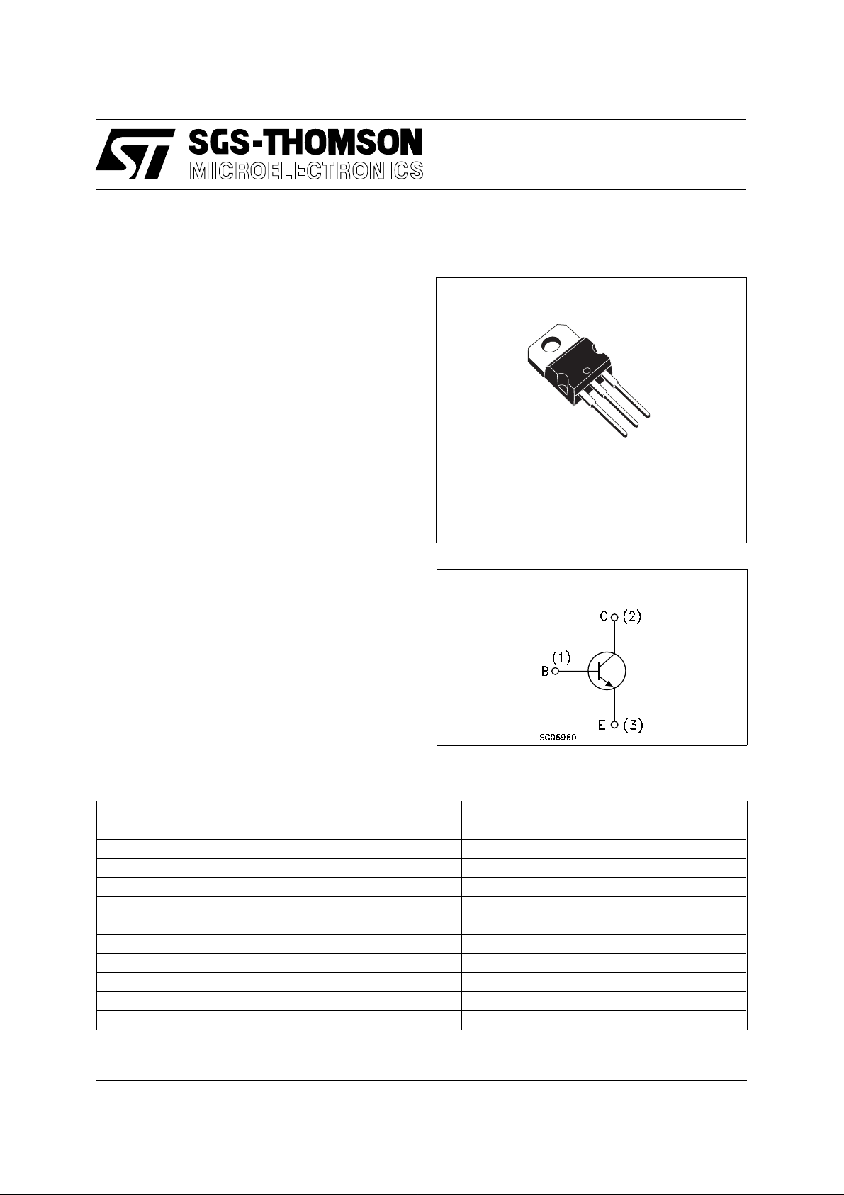
TO-220
BUV28
3
2
1
INTERNAL SCHEMATIC DIAGRAM
ABSOL UT E MAXIMU M RATINGS
Symbol Parameter Value Unit
V
V
V
I
I
P
P
T
Collector-base Voltage (IE = 0) 400 V
CBO
Collector-Emitter Voltage (IB = 0) 200 V
CEO
Emitter-Base Voltage (IC = 0) 7 V
EBO
Collector Current 10 A
I
C
Collector Peak Current 15 A
CM
Base Current 2 A
I
B
Base Peak Current 4 A
BM
Total Dissipation at Tc < 25 oC85W
tot
Total Dissipation at Tc < 60 oC65W
tot
Storage Temperature -65 to +175
stg
Max. Operating Junction Temperature 175
T
j
o
C
o
C
June 1997
1/4
Page 2
BUV28
THERMAL DATA
R
thj-case
Thermal Resistance Junction-case Max 1.76
o
C/W
ELECTRICAL CHARACTERISTICS (T
= 25 oC unless otherwise specified)
case
Symbol Parameter Test Conditions Min. Typ. Max. Unit
I
CER
I
CEX
Collector Cut-off
Current (R
= 50Ω)
BE
Collector Cut-off
= 400V T
V
CE
VCE = 400V
= 125oC3mA
c
= -1.5V Tc = 125oC1mA
VBE
Current
I
EBO
V
CEO(sus)
Emitter Cut-off
Current (I
= 0)
C
∗ Collector-Emitter
= 5 V 1 mA
V
EB
IC = 0.2 A L = 25mH 200 V
Sustaining Voltage
V
V
CE(sat)
V
BE(sat)
EBO
Emitter-Base
Voltage (I
∗ Collector-Emitter
Saturation Voltage
∗ Base-Emitter
= 0)
C
= 50mA 7 30 V
I
E
IC = 3A IB = 0.3A
I
= 6A IB = 0.6A
C
0.7
1.5
IC = 6A IB = 0.6A 2 V
Saturation Voltage
RESISTIVE LOAD
on
s
t
f
Storage Time
Fall Time
Turn-on Time
t
t
V
= 150V IC = 6A
CC
V
= - 6V IB1 = 0.6A
BE
R
= 5Ω
BB
0.3
0.5
0.1
1
1.5
0.25
INDUCTIVE LOAD
t
t
∗ Pulsed: Pulse duration = 300µs, duty cycle = 2 %
s
t
f
s
t
f
Storage time
Fall Time
Storage Time
Fall Time
V
= 150V IC = 6A
CC
I
= 0.6A VBE = - 5V
B1
L
=1µH
B
V
= 150V IC = 6A
CC
I
= 0.6A VBE = - 5V
B1
L
= 1µH Tj = 125oC
B
1
0.04
3
0.2
V
V
µs
µs
µs
µs
µs
µs
µs
2/4
Page 3

P011C
TO-220 MECHANICAL DATA
BUV28
DIM.
MIN. TYP. MAX. MIN. TYP. MAX.
A 4.40 4.60 0.173 0.181
C 1.23 1.32 0.048 0.051
D 2.40 2.72 0.094 0.107
D1 1.27 0.050
E 0.49 0.70 0.019 0.027
F 0.61 0.88 0.024 0.034
F1 1.14 1.70 0.044 0.067
F2 1.14 1.70 0.044 0.067
G 4.95 5.15 0.194 0.203
G1 2.4 2.7 0.094 0.106
H2 10.0 10.40 0.393 0.409
L2 16.4 0.645
L4 13.0 14.0 0.511 0.551
L5 2.65 2.95 0.104 0.116
L6 15.25 15.75 0.600 0.620
L7 6.2 6.6 0.244 0.260
L9 3.5 3.93 0.137 0.154
DIA. 3.75 3.85 0.147 0.151
mm inch
3/4
Page 4

BUV28
Information furnished is believed to be accurate and reliable. However, SGS-THOMSON Microelectronics assumes no responsability for the
consequences of use of such information nor for any infringement of pat e nts or ot her rights o f third partie s which may results from its use. No
license is granted by implication or otherwise under any patent or patent rights of SG S-THOMSON Microelectroni cs. Specifications ment ioned
in this publication are subject to cha nge wi t hout n o tice. This p u bli ca t ion sup e rsed e s and r epla ces al l inf ormat i on pr ev io us ly supplied.
SGS-THOMSON Microelectronics products are not auth orized for use as critical components in life support devices or systems without express
written approval of SGS-THOM SO N M icroelecto nics.
© 1997 SGS-THOMSON Microelectronics - Printed in Ita ly - All Right s Rese rved
Australia - Brazil - Canada - China - France - Germany - Italy - Japan - Korea - Malaysia - Malta - Morocco - The Netherlands -
Singapore - Spain - Sweden - Switzerland - Taiwan - Thailand - United Kingdom - U.S.A
SGS-THOMSON Microelectronics GROUP OF COMPANIES
. . .
4/4
 Loading...