

Page 1
HIGH CURR ENT NPN SILICON TRANSISTOR
■ SGS-THOMS O N PREF ERRE D SA LES TYP E
■ NPN TRANSISTOR
APPLICATIONS:
■ MOTOR CONTROL
■ HIGH FREQUENCY AND EFFICIENCY
CONVERTERS
BUTW92
DESCRIPTION
High current, high speed transistor suited for
power conversion applications, high efficency
converters and motor controls.
ABSOL UT E MAXIMU M RATINGS
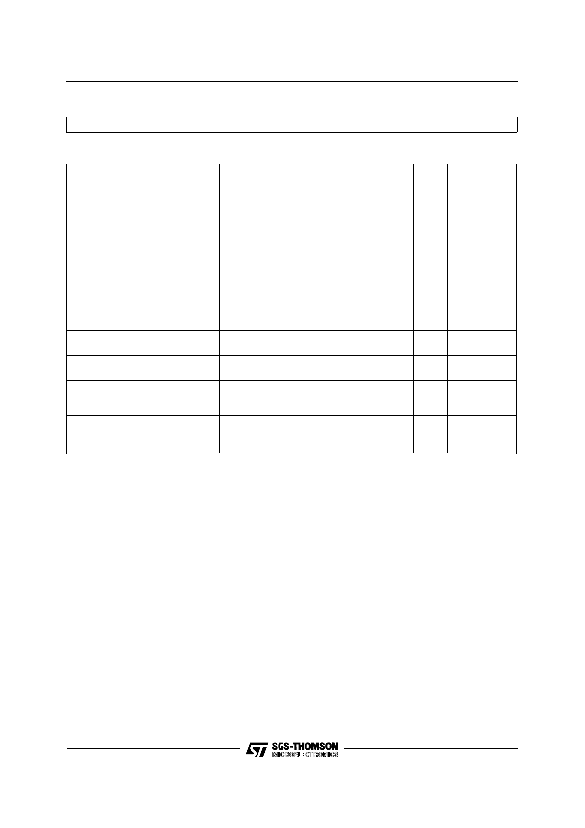
3
2
1
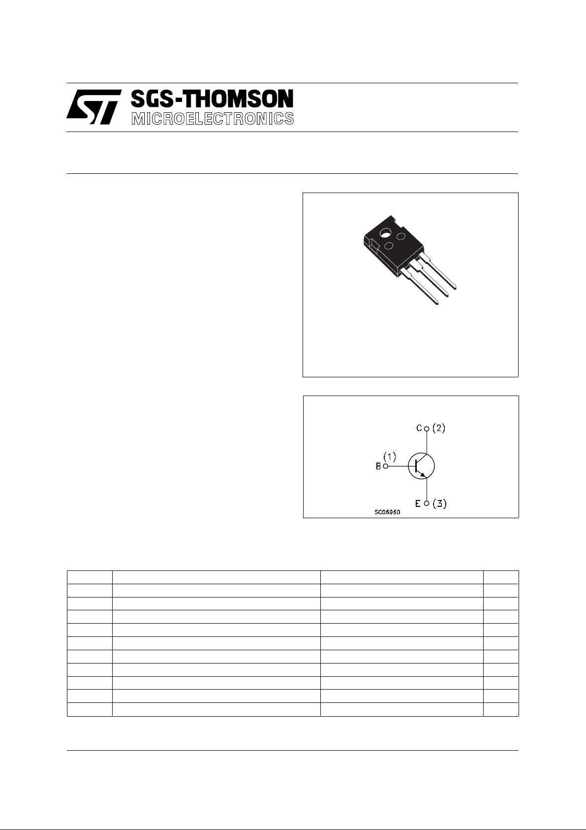
TO-247
INTERNAL SCHEMATIC DIAGRAM
Symbol Parameter Value Unit
V
V
V
I
I
P
T
For PNP type voltage and current values are negative.
Collector-Emitter Voltage (VBE = 0) 500 V
CES
Collector-Emitter Voltage (IB = 0) 250 V
CEO
Emitter-Base Voltage (IC = 0) 7 V
EBO
Emitter-Current 60 A
I
E
Emitter Peak Current (tp < 5ms) 70 A
EM
Base Current 15 A
I
B
Base Peak Current (tp < 5ms) 18 A
BM
Total Dissipation at Tc ≤ 25 oC 180 W
tot
Storage Temperature -65 to 150
stg
Max. Operating Junction Temperature 150
T
j
July 1997
o
C
o
C
1/4
Page 2
BUTW92
THERMAL DATA
R
thj-case
Thermal Resistance Junction-case MAX 0.7
o
C/W
ELECTRICAL CHARACTERISTICS (T
= 25 oC unless otherwise specified)
case
Symbol Parameter Test Conditions Min. Typ. Max. Unit
I
I
V
CES
EBO
CES
Collector Cut-off
Current (V
= -1.5V)
BE
Emitter Cut-off Current
(I
= 0)
C
Collector-Emitter
= 450 V
V
CE
= 450 V TC = 100oC
VCE
= 5 V 50 µA
V
EB
50
1
IC = 5 mA 500 V
Breakdown Voltage
(V
=0)
EB
V
EBO
Emitter-Base
I
= 50 mA 7 V
E
Breakdown Voltage
(I
= 0)
C
V
CEO(sus)
∗ Collector-Emitter
I
= 200 mA 250 V
C
Sustaining Voltage
(I
=0)
B
V
∗ Collector-Emitter
CE(sat)
Saturation Voltage
V
∗ Base-Emitter
BE(sat)
Saturation Voltage
h
∗ DC Current Gain IC = 60 A VCE = 3 V
FE
IC = 60 A IB = 15 A
I
= 60 A IB = 15 A TC = 100oC
C
IC = 60 A IB = 15 A
I
= 60 A IB = 15 A TC = 100oC
C
I
= 60 A VCE = 3 V TC = 100oC
C
I
= 5 A VCE = 3 V
C
0.8
1.1
1
1.5
1.9
2
9
6
65
RESISTIVE LOAD
t
∗ Pulsed: Pulse duration = 300 µs, duty cycle 1.5 %
s
t
f
Storage Time
Fall Time
I
= 50 A VCC = 250 V
C
I
= -IB2 = 10 A
B1
1.2
250
1.4
300
µA
mA
V
V
V
V
µs
ns
2/4
Page 3

TO-247 MECHANICAL DATA
BUTW92
DIM.
MIN. TYP. MAX. MIN. TYP. MAX.
A 4.7 5.3 0.185 0.209
D 2.2 2.6 0.087 0.102
E 0.4 0.8 0.016 0.031
F 1 1.4 0.039 0.055
F3 2 2.4 0.079 0.094
F4 3 3.4 0.118 0.134
G 10.9 0.429
H 15.3 15.9 0.602 0.626
L 19.7 20.3 0.776 0.779
L3 14.2 14.8 0.559 0.413 0.582
L4 34.6 1.362
L5 5.5 0.217
M 2 3 0.079 0.118
Dia 3.55 3.65 0.140 0.144
mm inch
P025P
3/4
Page 4

BUTW92
Information furnished is believed to be accurate and reliable. However, SGS-THOMSON Microelectronics assumes no responsability for the
consequences of use of such information nor for any infringement of pat e nts or ot her rights o f third partie s which may results from its use. No
license is granted by implication or otherwise under any patent or patent rights of SG S-THOMSON Microelectroni cs. Specifications ment ioned
in this publication are subject to cha nge wi t hout n o tice. This p u bli ca t ion sup e rsed e s and r epla ces al l inf ormat i on pr ev io us ly supplied.
SGS-THOMSON Microelectronics products are not auth orized for use as critical components in life support devices or systems without express
written approval of SGS-THOM SO N M icroele cton ics.
© 1997 SGS-THOMSON Microelectronics - Printed in Ita ly - All Rig hts Rese rved
Australia - Brazil - Canada - China - France - Germany - Italy - Japan - Korea - Malaysia - Malta - Morocco - The Netherlands -
Singapore - Spain - Sweden - Switzerland - Taiwan - Thailand - United Kingdom - U.S.A
SGS-THOMSON Microelectronics GROUP OF COMPANIES
. . .
4/4
 Loading...