

Page 1
®
■
STMicroelectronics PREFERRED
SALESTYPE
■
NPN TRANSISTOR
■
HIGH CURRENT CAPABILITY
■
FAST SWITCHING SPE ED
■
VERY LOW SATURATION VOLTAGE AND
HIGH GAIN
BUT70W
HIGH POWER NPN TRANSISTOR
APPLICATION
■
SWITCHING REGULATORS
■
MOTOR CONTROL
■
HIGH FREQUENCY AND EFFICENCY
CONVERTERS
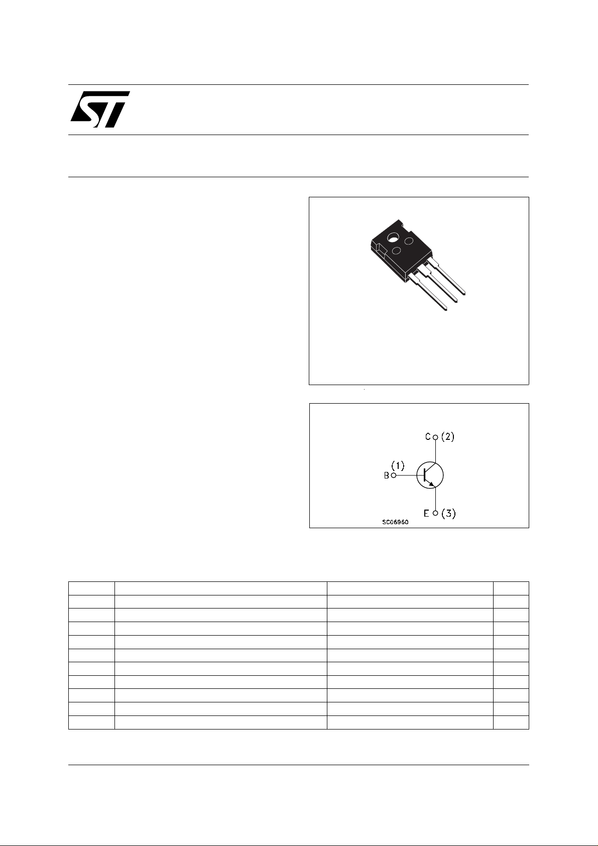
TO-247
3
2
1
DESCRIPTION
The BUT70W is a Multiepitaxial planar NPN
transistor in TO-247 plastic package.
It’s intented for use in high frequency and
efficiency converters such us motor controllers
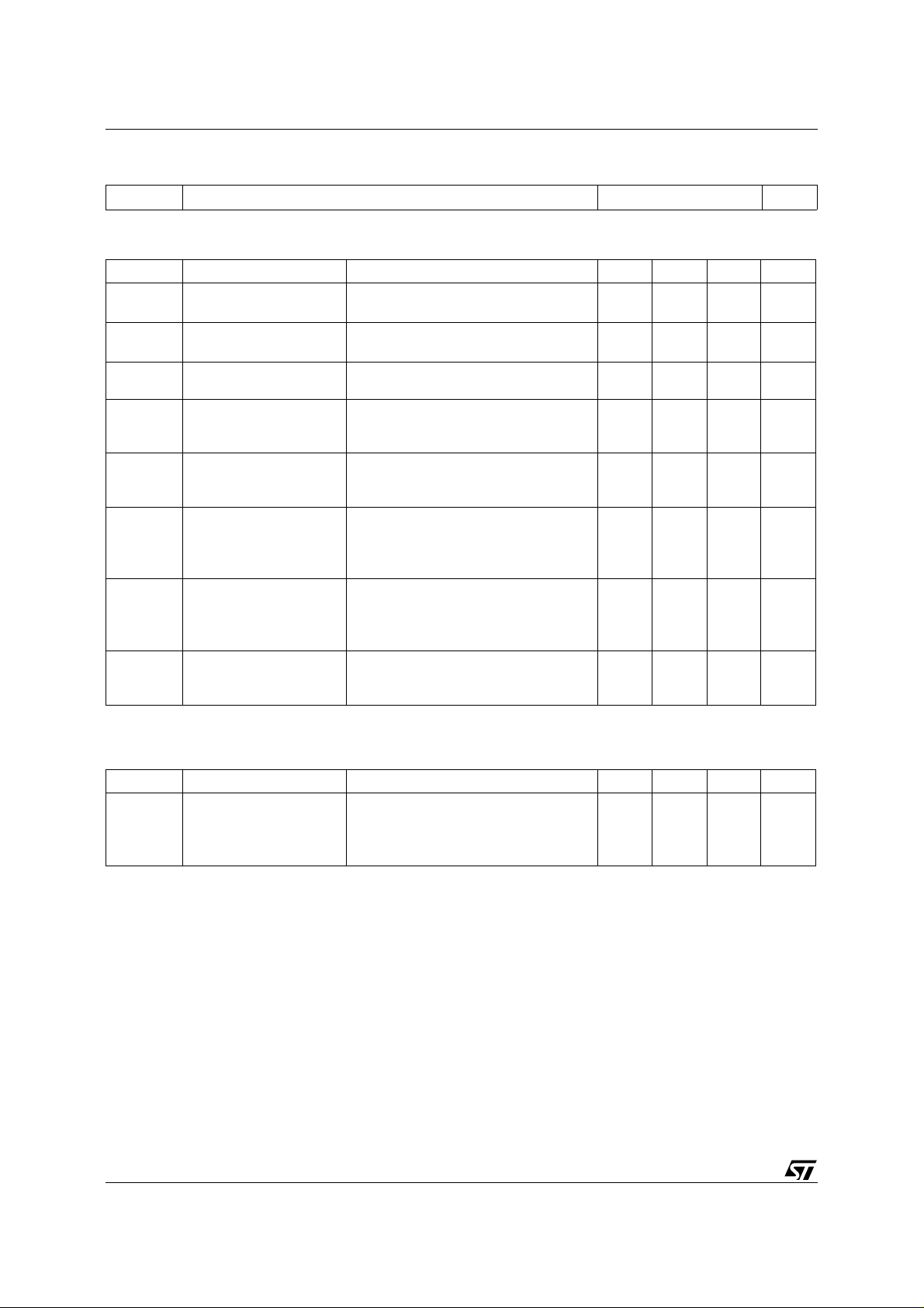
INTERNAL SCHEMATIC DIAGRAM
and industrial equipment.
ABSOLUTE MAXIMUM RATINGS
Symbol Parameter Value Unit
V
V
V
I
E(RMS)
I
I
P
T
Collector-emitter Voltage (VBE = -1.5V) 200 V
CEV
Collector-emitter Voltage (IB = 0) 125 V
CEO
Emitter-Base Voltage (IC = 0) 7 V
EBO
Emitter Current 40 A
Emitter Peak Current 120 A
EM
Base Current 8 A
I
B
Base Peak Current 24 A
BM
Total Power Dissipation at T
tot
Storage Temperature -65 to 150
stg
Max Operating Junction Temperature 150
T
j
case
< 25 oC
200 W
o
C
o
C
February 2002
1/4
Page 2
BUT70W
THERMAL DATA
R
thj-case
Thermal Resistance Junction-case Max 0.63
o
C/W
ELECTRICAL CHARACTERISTICS
= 25 oC unless otherwise specified)
(T
case
Symbol Parameter Test Conditions Min. Typ. Max. Unit
I
CER
I
CEV
I
EBO
V
CEO(sus)
Collector Cut-off
Current (R
= 5Ω)
BE
Collector Cut-off
Current (V
= -1.5V)
BE
Emitter Cut-off
Current (I
= 0)
C
∗ Collector-Emitter
V
= 200 V
CE
V
= 200 V TC = 100oC
CE
= 200 V
V
CE
V
= 200 V TC = 100oC
CE
= 5 V 1 mA
V
EB
I
= 0.2 A L = 25 mH 125 V
C
1
5
1
4
Sustaining Voltage
(I
= 0)
B
V
(BR)EBO
Emitter-Base
I
= 50 mA 7 V
E
Breakdown Voltage
(I
= 0)
C
V
∗ Collector-Emitter
CE(sat)
Saturation Voltage
V
∗ Base-Emitter
BE(sat)
Saturation Voltage
di
∗ Rated of Rise of
c/dt
on-state Collector
= 70 A IB = 7 A
I
C
I
= 70 A IB = 7 A TC = 100oC
C
I
= 35 A IB = 1.75 A
C
I
= 35 A IB = 1.75 A TC = 100oC
C
= 70 A IB = 7 A
I
C
I
= 70 A IB = 7 A TC = 100oC
C
I
= 35 A IB = 1.75 A
C
I
= 35 A IB = 1.75 A TC = 100oC
C
V
= 100 V RC = 0 IB1 = 3.5 A
CC
= 3 µs TC = 100oC
t
p
140 A/µs
0.9
1.5
0.9
1.2
1.8
1.9
1.4
1.4
Current
∗
Pulsed: Pulse duration = 300 µs, duty cycle < 2 %
mA
mA
mA
mA
V
V
V
V
V
V
V
V
INDUCTIVE LOAD
Symbol Parameter Test Conditions Min. Typ. Max. Unit
1.8
0.2
0.35
2/4
t
t
Storage Time
s
Fall Time
t
f
Cross Over Time
c
IC = 35 A VCC = 90 V
= -5 V RB2 = 1.4 Ω
V
BB
= 1.75 A LC = 0.15 mH
Ι
B1
V
= 125V TC = 100oC
CLAMP
µs
µs
µs
Page 3

TO-247 MECHANICAL DATA
BUT70W
DIM.
MIN. TYP. MAX. MIN. TYP. MAX.
A 4.7 5.3 0.185 0.209
D 2.2 2.6 0.087 0.102
E 0.4 0.8 0.016 0.031
F 1 1.4 0.039 0.055
F3 2 2.4 0.079 0.094
F4 3 3.4 0.118 0.134
G 10.9 0.429
H 15.3 15.9 0.602 0.626
L 19.7 20.3 0.776 0.779
L3 14.2 14.8 0.559 0.582
L4 34.6 1.362
L5 5.5 0.217
M 2 3 0.079 0.118
mm inch
P025P
3/4
Page 4

BUT70W
Information furnished is believed to be accurate and reliable. However, STMicroelectronics assumes no responsibility for the consequences
of use of such inform ation nor for any in fringe ment o f patents or other rig hts of third par ties wh ich may result from its u se. N o li cen se is
granted by implication or otherwise under any patent or patent rights of STMicroelectronics. Specification mentioned in this publication are
subject to change without notice. This publication supersedes and replaces all information previously supplied. STMicroelectronics products
are not authorized f or use as critical components in life support devices or systems without express written approval of STMicroelectronics.
The ST logo is a trademark of STMicroelectronics
© 2002 STMicroelectro nics – Printed in Italy – All Rights Reserved
STMicroelectronics GROUP OF COMPANIES
Australia - Brazil - Canada - China - Finland - France - Germany - Hong Kong - India - Israel - Italy - Japan - Malaysia - Malta - Morocco -
Singapore - Spain - Sweden - Switzerland - United Kingdom - United States.
http://www.st.com
4/4
 Loading...