

Page 1
HIGH POWER NPN SILICON TRANSISTOR
■ SGS-THOMS O N PREF ERRE D SA LES TYP E
■ NPN TRANSISTOR
■ HIGH CURRENT CAPABILITY
■ FAST SWITCHING SPEED
■ VERY LOW SATURATION VOLTAGE AND
HIGH GAIN
APPLICATION
■ SWITCHING REGULATOR S
■ MOTOR CONTROL
■ HIGH FREQU E NCY AND EF FICE N CY
CONVERTERS
DESCRIPTION
The BUT70 is a Multiepitaxial planar NPN
transistor in TO-218 plastic package.
It’s intented for use in high frequency and
efficiency converters such us motor controllers
and industrial equipment.
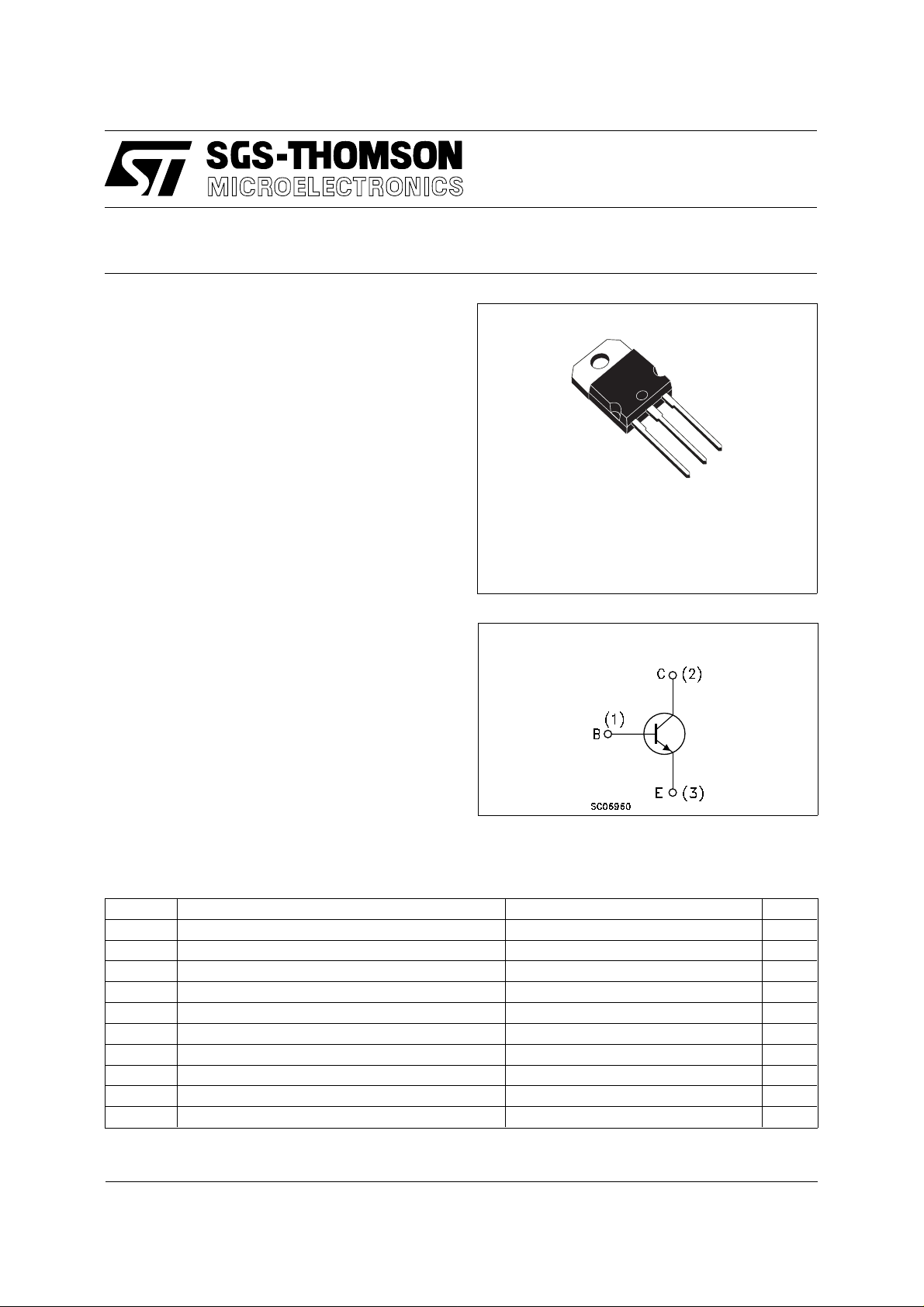
BUT70
3
2
1
TO-218
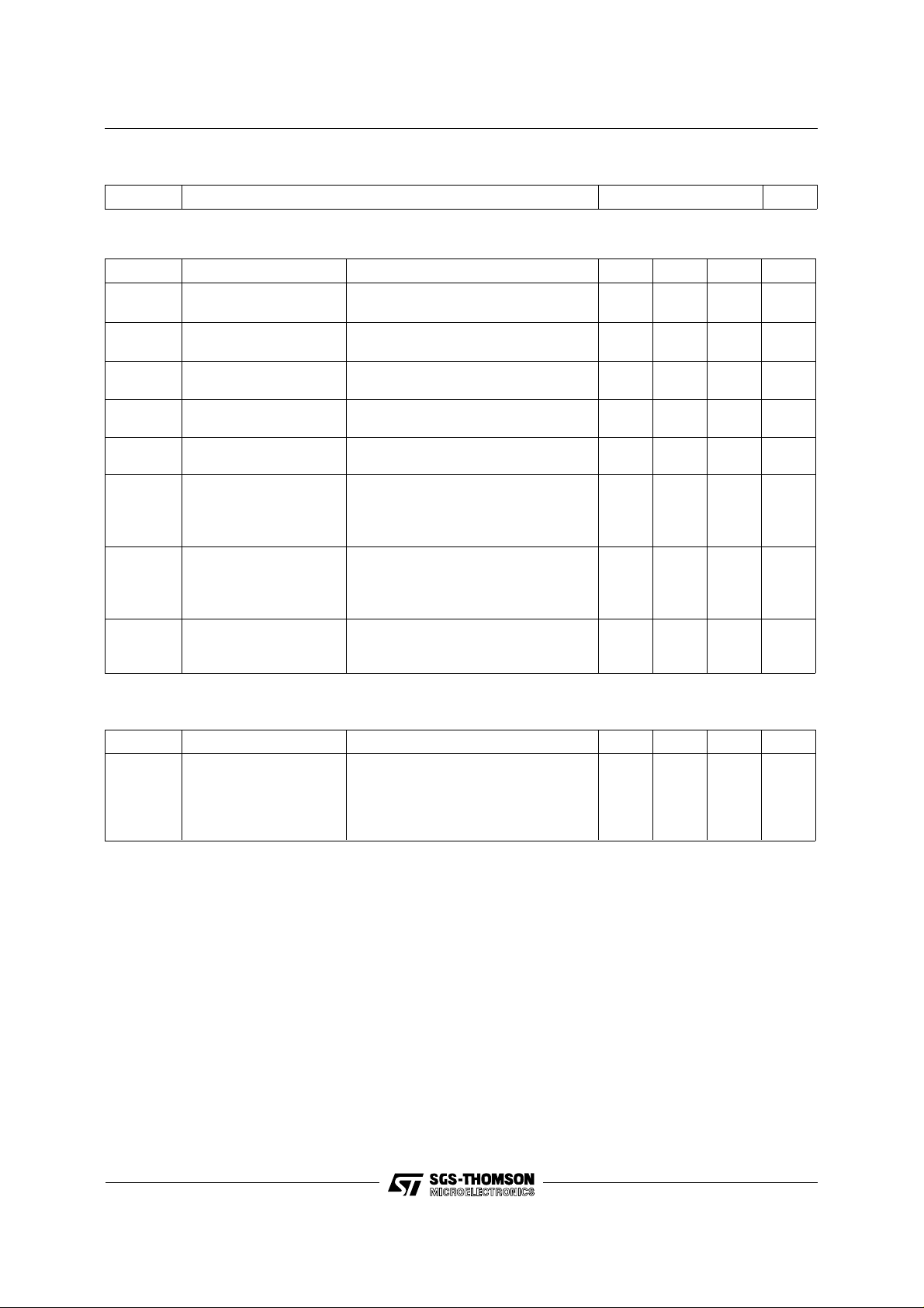
INTERNAL SCHEMATIC DIAGRAM
ABSOLUT E MAXIMUM RATI NG S
Symbol Parameter Value Unit
V
V
V
I
E(RMS)
I
I
P
T
July 1997
Collector-emitter Voltage (VBE = -1.5V) 200 V
CEV
Collector-emitter Voltage (IB = 0) 125 V
CEO
Emitter-Base Voltage (IC = 0) 7 V
EBO
Emitter Current 40 A
Emitter Peak Current 120 A
EM
Base Current 8 A
I
B
Base Peak Current 24 A
BM
Total Power Dissipation at T
tot
Storage Temperature -65 to 150
stg
Max Operating Junction Temperature 150
T
j
< 25 oC 200 W
case
o
C
o
C
1/4
Page 2
BUT70
THERMAL DATA
R
thj-case
Thermal Resistance Junction-case Max 0.63
o
C/W
ELECTRICAL CHARACTERISTICS (T
= 25 oC unless otherwise specified)
case
Symbol Parameter Test Conditions Min. Typ. Max. Unit
I
CER
I
CEV
I
EBO
V
CEO(sus)
V
V
CE(sat)
V
BE(sat)
di
c/dt
EBO
Collector Cut-off
Current (R
= 5Ω)
BE
Collector Cut-off
Current
Emitter Cut-off
Current (I
= 0)
C
∗ Collector-Emitter
Sustaining Voltage
Emitter-base
Voltage (I
= 0)
C
∗ Collector-Emitter
Saturation Voltage
∗ Base-Emitter
Saturation Voltage
∗ Rated of Rise of
on-state Collector
= V
V
CE
VCE = V
VCE = V
V
V
IC = 0.2A
CEV
Tc = 100oC
CEV
CEV VBE
= V
CE
CEV VBE
= - 5 V 1 mA
EB
= -1.5V
= - 1.5V TC =100oC
125 V
1
5
1
4
L = 25 mH
= 50 mA 7 V
I
E
IC = 70 A IB = 7 A
I
= 70 A IB = 7 A Tj = 100oC
C
I
= 35 A IB = 1.75 A
C
I
= 35 A IB = 1.75 A Tj = 100oC
C
IC = 70 A IB = 7 A
I
= 70 A IB = 7 A Tj = 100oC
C
I
= 35 A IB = 1.75 A
C
I
= 35 A IB = 1.75 A Tj = 100oC
C
V
= 100 V RC = 0 IB1 = 3.5 A
CC
t
=3 µS Tj = 100oC
p
140 A/µs
0.9
1.5
0.9
1.2
1.8
1.9
1.4
1.4
Current
∗ Pulsed: Pulse duration = 300 µs, duty cycle < 2 %
mA
mA
mA
mA
V
V
V
V
V
V
V
V
INDUCTIVE LOAD
Symbol Parameter Test Conditions Min. Typ. Max. Unit
t
Rise Time
r
s
t
f
Storage Time
Fall Time
t
V
= 90 V IC = 35 A
CC
V
= -5 V IB1 = 1.75 A
BB
R
= 1.4 Ω
B2
L
=0.13 mH TJ =100oC
C
V
=125V
CLAMP
1.8
0.2
0.35
µs
µs
µs
2/4
Page 3

TO-218 (SOT-93) MECHANICAL DATA
BUT70
DIM.
MIN. TYP. MAX. MIN. TYP. MAX.
A 4.7 4.9 0.185 0.193
C 1.17 1.37 0.046 0.054
D2.5 0.098
E 0.5 0.78 0.019 0.030
F 1.1 1.3 0.043 0.051
G 10.8 11.1 0.425 0.437
H 14.7 15.2 0.578 0.598
L2 – 16.2 – 0.637
L3 18 0.708
L5 3.95 4.15 0.155 0.163
L6 31 1.220
R – 12.2 – 0.480
Ø 4 4.1 0.157 0.161
mm inch
H
A
C
L5
E
D
L6
L3
L2
G
¯
F
R
1
2 3
P025A
3/4
Page 4

BUT70
Information furnished is believed to be accurate and reliable. However, SGS-THOMSON Microelectronics assumes no responsability for the
consequences of use of such information nor for any infringement of pat e nts or ot her rights o f third partie s which may results from its use. No
license is granted by implication or otherwise under any patent or patent rights of SG S-THOMSON Microelectroni cs. Specifications ment ioned
in this publication are subject to cha nge wi t hout n o tice. This p u bli ca t ion sup e rsed e s and r epla ces al l inf ormat i on pr ev io us ly supplied.
SGS-THOMSON Microelectronics products are not auth orized for use as critical components in life support devices or systems without express
written approval of SGS-THOM SO N M icroele cton ics.
© 1997 SGS-THOMSON Microelectronics - Printed in Ita ly - All Rig hts Rese rved
Australia - Brazil - Canada - China - France - Germany - Italy - Japan - Korea - Malaysia - Malta - Morocco - The Netherlands -
Singapore - Spain - Sweden - Switzerland - Taiwan - Thailand - United Kingdom - U.S.A
SGS-THOMSON Microelectronics GROUP OF COMPANIES
. . .
4/4
 Loading...