

Page 1
HIGH POWER NPN SILICON TRANSISTOR
■ SGS-THOMS O N PREF ERRE D SA LES TYP E
■ NPN TRANSISTOR
■ HIGH CURRENT CAPABILITY
■ FAST SWITCHING SPEED
■ HIGH RUGG E DN ES S
APPLICATION
■ MOTOR CONTROL
■ UNINTERRUPTAB LE POWE R SUP PLY
DESCRIPTION
The BUT100 is a Multiepitaxial Planar NPN
Transistor in TO-3 package. It is intended for use
in high frequency and efficency converters,
switching regulators and motor control.
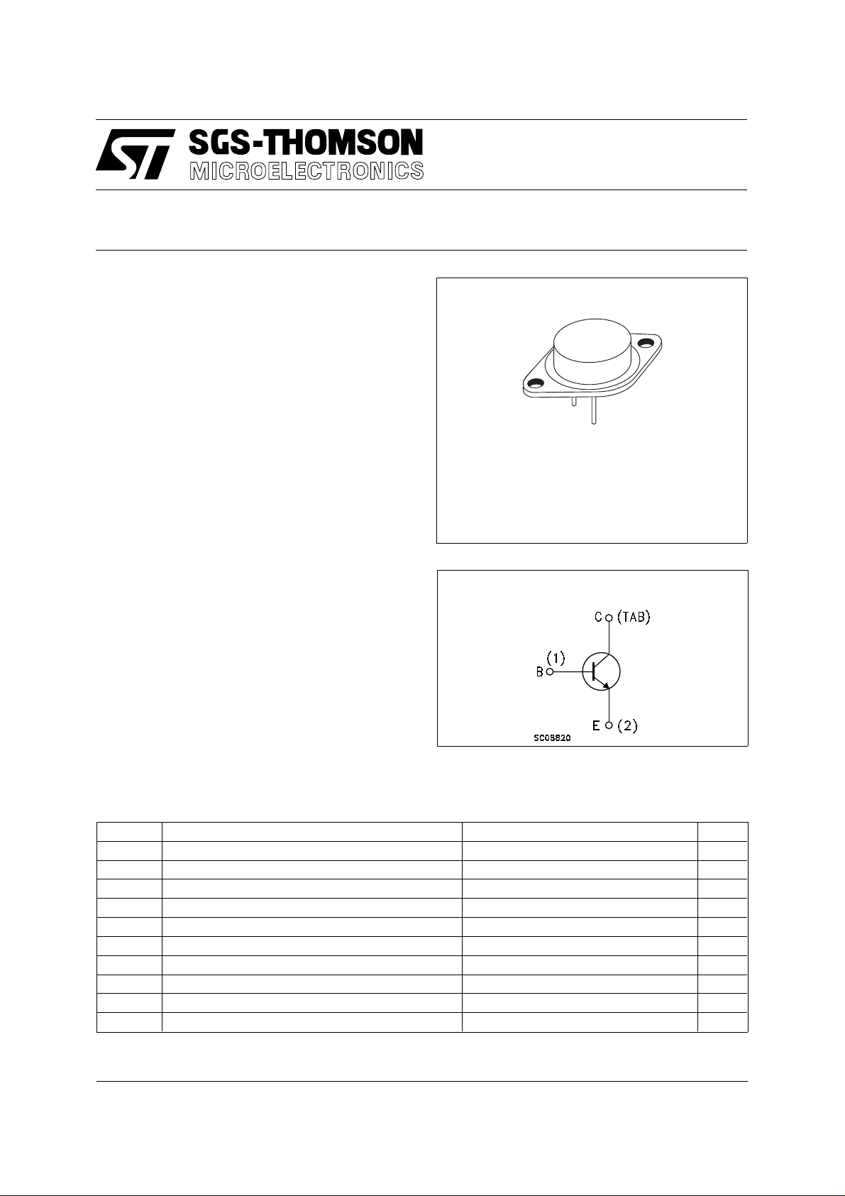
BUT100
1
2
TO-3
(version " S ")
INTERNAL SCHEMATIC DIAGRAM
ABSOL UT E MAXIMU M RATINGS
Symbol Parameter Value Unit
V
V
V
I
I
P
T
Collector-Emitter Voltage (VBE = -1.5V) 200 V
CEV
Collector-Emitter Voltage (IB = 0) 125 V
CEO
Emitter-Base Voltage (IC = 0) 7 V
EBO
Emitter Current 50 A
I
E
Emitter Peak Current 150 A
EM
Base Current 10 A
I
B
Base Peak Current 30 A
BM
Total Dissipation at Tc < 25 oC 300 W
tot
Storage Temperature -65 to 200
stg
Max. Operating Junction Temperature 200
T
j
o
C
o
C
April 1997
1/4
Page 2

BUT100
THERMAL DATA
R
thj-case
Thermal Resistance Junction-case Max 0.58
o
C/W
ELECTRICAL CHARACTERISTICS (T
= 25 oC unless otherwise specified)
case
Symbol Parameter Test Conditions Min. Typ. Max. Unit
I
CER
I
CEV
I
EBO
V
CEO(sus)
V
V
CE(sat)
V
BE(sat)
di
EBO
c
Collector Cut-off
Current (R
= 5Ω)
BE
Collector Cut-off
Current
Emitter Cut-off Current
(I
= 0)
C
∗ Collector-Emitter
Sustaining Voltage
Emitter-Base Voltage
(I
= 0)
C
∗ Collector-Emitter
Saturation Voltage
∗ Base-Emitter
Saturation Voltage
/dt Rate of Rise of
on-state Collector
= V
V
CE
V
VCE = V
V
V
IC = 0.2 A
CEV
= V
CE
CEV TC
CEV VBE
= V
CE
CEV VBE
= 5 V 1 mA
EB
= 100oC
= -1.5V
= -1.5V TC = 100oC
125 V
1
5
1
4
L = 25mH
= 50mA 7 V
I
E
IC = 50A IB = 2.5A
I
= 100A IB = 10A
C
I
= 50A IB = 2.5A Tj = 100oC
C
I
= 100A IB = 10A Tj = 100oC
C
IC = 50A IB = 2.5A
I
= 100A IB = 10A
C
I
= 50A IB = 2.5A Tj = 100oC
C
I
= 100A IB = 10A Tj = 100oC
C
V
= 100V RC = 0 IB1 = 5A
CC
T
= 3µs Tj = 100oC
p
180 A/µs
0.9
0.9
1.2
1.5
1.4
2
1.4
2.1
Current
INDUCTIVE LOAD
s
t
f
c
Storage time
Fall Time
Crossover Time
t
t
V
= 90V V
CC
I
= 50A IB1 = 2.5A
C
V
= - 5V LC = 80µH
BB
R
= 1 Ω Tj = 100oC
B2
clamp
= 125 V
2
0.2
0.35
mA
mA
mA
mA
V
V
V
V
V
V
V
V
µs
µs
µs
V
CEW
Maximum Collector
Emitter Voltage
without Snubber
∗ Pulsed: Pulse duration = 3µs, duty cycle = 2 %
2/4
V
= 90V I
CC
= - 5V IB1 = 10A
VBB
L
= 30µH RB2 = 1Ω
C
T
= 125oC
j
CWoff =
150A
125 V
Page 3

P003O
TO-3 (version S) MECHANICAL DATA
BUT100
DIM.
MIN. TYP. MAX. MIN. TYP. MAX.
A 11.00 13.10 0.433 0.516
B 1.47 1.60 0.058 0.063
C 1.50 1.65 0.059 0.065
D 8.32 8.92 0.327 0.351
E 19.00 20.00 0.748 0.787
G 10.70 11.10 0.421 0.437
N 16.50 17.20 0.649 0.677
P 25.00 26.00 0.984 1.023
R 4.00 4.09 0.157 0.161
U 38.50 39.30 1.515 1.547
V 30.00 30.30 1.187 1.193
mm inch
P
A
G
U
V
N
O
B
D
C
E
R
3/4
Page 4

BUT100
Information furnished is believed to be accurate and reliable. However, SGS-THOMSON Microelectronics assumes no responsability for the
consequences of use of such information nor for any infringement of patents or other rights of third parties which may results from its use. No
license is granted by implication or ot h erwise under any patent or patent rights of SGS-THOMSON Microelectronics. Specifi cations mentioned
in this publication are subject to change without notice. This publication sup ersedes and replaces all information previously supplied.
SGS-THOMSON Microelectronics products are not authorized for use as critical components in life support devices or systems without express
written approval of SGS-THOMSON Microelectonics.
© 1997 SGS-THOMSON Microelectronics - Printed in Italy - All Rights Reserved
Australia - Brazil - Canada - China - France - Germany - Hong Kong - Italy - Japan - Korea - Malaysia - Malta - Morocco - The Netherlands -
Singapore - Spain - Sweden - Switzerland - Taiwan - Thailand - United Kingdom - U.S.A
SGS-THOMSON Microelectronics GROUP OF COMPANIES
. . .
4/4
 Loading...