

Page 1
BULD25D, BULD25DR, BULD25SL
E
NPN SILICON TRANSISTOR WITH INTEGRATED DIODE
JULY 1994 - REVISED SEPTEMBER 1997Copyright © 1997, Power Innovations Limited, UK
● Designed Specifically for High Frequency
Electronic Ballasts
● Integrated Fast t
Anti-parallel Diode,
rr
Enhancing Reliability
● Diode t
● New Ultra Low-Height SOIC Power Package
● Tightly Controlled Transistor Storage Times
● Voltage Matched Integrated Transistor and
Typically 500 ns
rr
Diode
● Characteristics Optimised for Cool Running
● Diode-Transistor Charge Coupling
Minimised to Enhance Frequency Stability
● Custom Switching Selections Available
● Surface Mount and Through-Hole Options
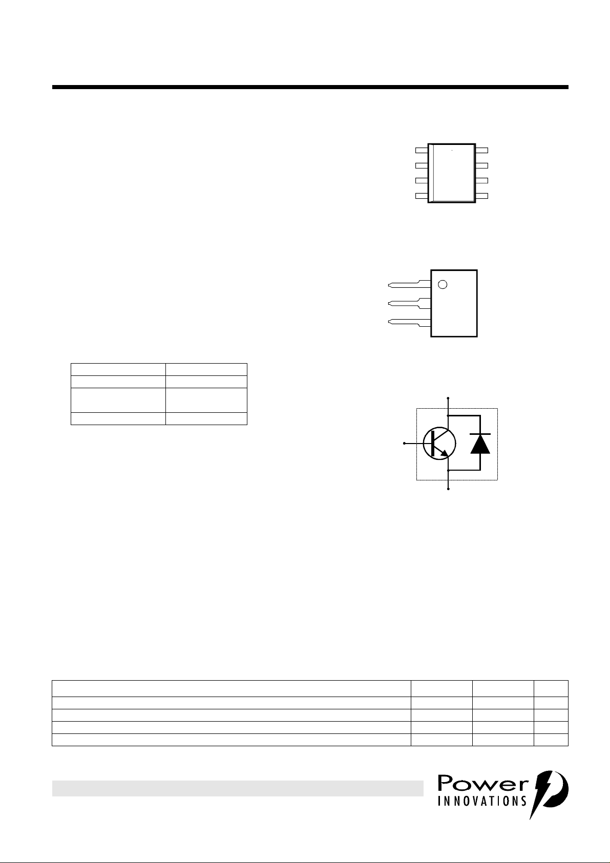
PACKAGE PART # SUFFIX
Small-outline D
Small-outline taped
and reeled
Single-in-line SL
DR
B
C
E
device symbol
D PACKAGE
(TOP VIEW)
1
B
E
SL PACKAGE
2
3
4 5
(TOP VIEW)
1
2
3
NC
NC
NC - No internal connection
8 C
7
6
C
C
C
C
B
description
The new BULDxx range of transistors have been
designed specifically for use in High Frequency
Electronic Ballasts (HFEB’s). This range of
switching transistors has tightly controlled
storage times and an integrated fast trr anti-parallel diode. The revolutionary design ensures that the diode
has both fast forward and reverse recovery times, achieving the same performance as a discrete anti-parallel
diode plus transistor.
The integrated diode has minimal charge coupling with the transistor, increasing frequency stability,
especially in lower power circuits where the circulating currents are low. By design, this new device offers a
voltage matched integrated transistor and anti-parallel diode.
This device is available in the now well established 8 pin low height surface mount D package, and the TO220 pin compatible SL package. Use of the SL package allows for a 40% height saving, making it ideal for
compact ballast applications.
absolute maximum ratings at 25°C ambient temperature (unless otherwise noted)
RATING SYMBOL VALUE UNIT
Collector-emitter voltage (V
Collector-base voltage (I
Collector-emitter voltage (I
Emitter-base voltage V
= 0) V
BE
= 0) V
E
= 0) V
B
CES
CBO
CEO
EBO
600 V
600 V
400 V
9 V
PRODUCT INFORMATION
Information is current as of publication date. Products conform to specifications in accordance
with the terms of Power Innovations standard warranty. Production processing does not
necessarily include testing of all parameters.
1
Page 2
BULD25D, BULD25DR, BULD25SL
NPN SILICON TRANSISTOR WITH INTEGRATED DIODE
JULY 1994 - REVISED SEPTEMBER 1997
absolute maximum ratings at 25°C ambient temperature (unless otherwise noted) (continued)
RATING SYMBOL VALUE UNIT
Continuous collector current (see Note 1) I
Peak collector current (see Note 2) I
Continuous base current (see Note 1) I
Peak base current (see Note 2) I
Continuous device dissipation at (or below) 25°C ambient temperature
BULD25D
BULD25SL
Maximum average continuous diode forward current at (or below) 25°C ambient temperature I
Operating junction temperature range T
Storage temperature range T
NOTES:1. This value applies for t
2. This value applies for t
= 1 s.
p
= 10 ms, duty cycle ≤ 2%.
p
electrical characteristics at 25°C ambient temperature
PARAMETER TEST CONDITIONS MIN TYP MAX UNIT
CES
EBO
FE
EC
Collector-emitter
sustaining voltage
Collector-emitter
cut-off current
Emitter cut-off
current
Base-emitter
saturation voltage
Collector-emitter
saturation voltage
Forward current
transfer ratio
Anti-parallel diode
forward voltage
V
CEO(sus)
I
I
V
BE(sat)
V
CE(sat)
h
V
NOTES: 3. These parameters must be measured using pulse techniques, t
4. These parameters must be measured using voltage-sensing contacts, separate from the current carrying contacts, and located
within 1 mm from the device body for the D package and 3.2 mm from the device body for the SL package.
= 0.1 A 400 V
I
C
= 600 V VBE= 0 10 µA
V
CE
= 9 V IC= 0 1 mA
V
EB
= 0.1 A IC= 0.5 A (see Notes 3 and 4) 0.9 1.1 V
I
B
IB = 0.1 A
= 0.2 A
I
B
V
= 10 V
CE
= 1.5 V
V
CE
= 5 V
V
CE
= 1 A (see Notes 3 and 4) 1.5 1.7 V
I
E
I
= 0.5 A
C
= 1 A
I
C
I
= 0.01 A
C
= 0.5 A
I
C
= 1 A
I
C
(see Notes 3 and 4)
(see Notes 3 and 4)1010
= 300 µs, duty cycle ≤ 2%.
p
C
CM
B
BM
P
tot
E(av)
stg
j
10
2 A
4 A
1.5 A
2.5 A
see Figure 10
see Figure 11
0.5 A
-65 to +150 °C
-65 to +150 °C
0.3
0.5
0.6
1
18
15
15
20
20
W
V
thermal characteristics
PARAMETER MIN TYP MAX UNIT
R
Junction to free air thermal resistance
θJA
D package
SL Package
switching characteristics at 25°C ambient temperature
PARAMETER TEST CONDITIONS MIN TYP MAX UNIT
Anti-parallel diode
t
rr
reverse recovery time
Storage time (see Note 5) 2 3.5 5 µs
t
s
Fall time (see Note 5) 0.25 0.35 µs
t
f
Measured by holding transistor
in an off condition, V
= -3 V
EB
(see Note 5) 0.5 1 µs
NOTE 5: Refer to Figures 12, 13 and 14 for Functional Test Circuit and Switching Waveforms.
PRODUCT INFORMATION
2
165
115
°C/W
Page 3
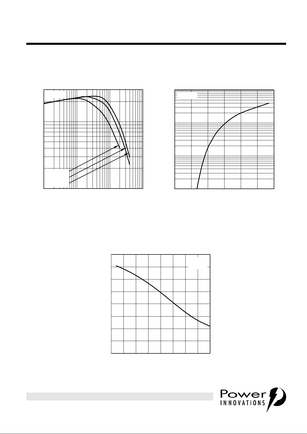
TYPICAL CHARACTERISTICS
FORWARD CURRENT TRANSFER RATIO
vs
COLLECTOR CURRENT
30
TA = 25°C
BULD25D, BULD25DR, BULD25SL
NPN SILICON TRANSISTOR WITH INTEGRATED DIODE
JULY 1994 - REVISED SEPTEMBER 1997
ANTI-PARALLEL DIODE
INSTANTANEOUS FORWARD CURRENT
vs
LDX25SHF
INSTANTANEOUS FORWARD VOLTAGE
10
TA = 25°C
LDX25DVF
10
- Forward Current Transfer Ratio
FE
h
VCE = 1.5 V
VCE = 5 V
VCE = 10 V
1·0
0·01 0·1 1·0 10
IC - Collector Current - A
Figure 1. Figure 2.
BASE-EMITTER SATURATION VOLTAGE
AMBIENT TEMPERATURE
1.0
1·0
0·1
- Instantaneous Forward Current - A
E
I
0·01
0 0·5 1·0 1·5 2·0 2·5 3·0
VEC - Instantaneous Forward Voltage - V
vs
LDX25SVB
IC = 0.5 A
IB = 0.1 A
0.9
0.8
0.7
- Base-Emitter Saturation Voltage - V
BE(sat)
V
0.6
-50 -25 0 25 50 75 100 125 150
TA - Ambient Temperature - °C
PRODUCT INFORMATION
Figure 3.
3
Page 4
BULD25D, BULD25DR, BULD25SL
NPN SILICON TRANSISTOR WITH INTEGRATED DIODE
JULY 1994 - REVISED SEPTEMBER 1997
MAXIMUM SAFE OPERATING REGIONS
MAXIMUM FORWARD-BIAS
SAFE OPERATING AREA
10
BULD25D
TA = 25°C
1·0
- Collector Current - A
0·1
C
I
tp = 100 µs
tp = 10 ms
tp = 1 s
0·01
1·0 10 100 1000
VCE - Collector-Emitter Voltage - V
Figure 4. Figure 5.
LDX25DFB
MAXIMUM FORWARD-BIAS
SAFE OPERATING AREA
10
BULD25SL
TA = 25°C
1·0
- Collector Current - A
0·1
C
I
tp = 100 µs
tp = 10 ms
tp = 1 s
0·01
1·0 10 100 1000
VCE - Collector-Emitter Voltage - V
LDX25SFB
MAXIMUM REVERSE-BIAS
SAFE OPERATING AREA
5
BULD25D
I
= IC / 5
B(on)
V
4
3
2
- Collector Current - A
C
I
1
0
0 100 200 300 400 500 600 700 800
VCE - Collector-Emitter Voltage - V
BE(off)
TA = 25°C
Figure 6. Figure 7.
LDX25DRB
= -5 V
MAXIMUM REVERSE-BIAS
SAFE OPERATING AREA
5
BULD25SL
I
= IC / 5
B(on)
V
4
3
2
- Collector Current - A
C
I
1
0
0 100 200 300 400 500 600 700 800
VCE - Collector-Emitter Voltage - V
BE(off)
TA = 25°C
LDX25SRB
= -5 V
PRODUCT INFORMATION
4
Page 5

1·0
0·1
60%
40%
20%
10%
BULD25D, BULD25DR, BULD25SL
NPN SILICON TRANSISTOR WITH INTEGRATED DIODE
JULY 1994 - REVISED SEPTEMBER 1997
THERMAL INFORMATION
THERMAL RESPONSE JUNCTION TO AMBIENT
vs
POWER PULSE DURATION
LDX25DZA
BULD25D
TA = 25°C
0·01
- Normalised Transient Thermal Impedance
θ
θJA
0%
/R
θ
θJA
Z
0·001
10
-4
10
-3
10
-2
THERMAL RESPONSE JUNCTION TO AMBIENT
1·0
0·1
60%
40%
20%
10%
duty cycle = t1/t2
Read time at end of t1,
T
Jmax()TAPDpeak()
10
-1
10
0
t1 - Power Pulse Duration - s
Figure 8.
vs
POWER PULSE DURATION
10
1
Z
θJA
R
θJA
t1
t2
R
••=–
θJAmax()
2
10
BULD25SL
TA = 25°C
LDX25SZA
10
3
0·01
0%
- Normalised Transient Thermal Impedance
θ
θJA
/R
θ
θJA
Z
0·001
10
-4
10
-3
10
-2
t1 - Power Pulse Duration - s
PRODUCT INFORMATION
duty cycle = t1/t2
Read time at end of t1,
T
Jmax()TAPDpeak()
-1
10
Figure 9.
10
t1
t2
Z
θJA
R
0
10
1
θJA
10
••=–
2
R
θJAmax()
10
3
5
Page 6

BULD25D, BULD25DR, BULD25SL
NPN SILICON TRANSISTOR WITH INTEGRATED DIODE
JULY 1994 - REVISED SEPTEMBER 1997
THERMAL INFORMATION
MAXIMUM POWER DISSIPATION JUNCTION TO AMBIENT
vs
POWER PULSE DURATION
100
10
10%
20%
40%
60%
1·0
- Maximum Power Dissipation - W
tot
P
0%
LDX25DPA
BULD25D
TA = 25°C
0·1
10
-4
10
-3
MAXIMUM POWER DISSIPATION JUNCTION TO AMBIENT
100
10%
10
20%
40%
- Maximum Power Dissipation - W
tot
P
60%
0%
10
-2
10
-1
t1 - Power Pulse Duration - s
Figure 10.
vs
POWER PULSE DURATION
10
0
10
1
10
2
LDX25SPA
10
3
BULD25SL
TA = 25°C
1·0
10
-4
10
-3
10
-2
t1 - Power Pulse Duration - s
PRODUCT INFORMATION
6
-1
10
Figure 11.
10
0
10
1
10
2
10
3
Page 7

0V
V = 325 V
s
BULD25
R
B
BULD25D, BULD25DR, BULD25SL
NPN SILICON TRANSISTOR WITH INTEGRATED DIODE
JULY 1994 - REVISED SEPTEMBER 1997
FUNCTIONAL TEST CIRCUIT
C
slew
N
s
R
B
R
E
N
p
T2
L1
R
load
C
coupling
C
filter
BULD25
N
s
R
E
IDDATBAL
Figure 12.
COMPONENT VALUES USED IN
FUNCTIONAL TEST CIRCUIT
R
B
R
E
R
load
C
coupling
C
slew
C
filter
L1 2.5 mH
: N
T2 N
P
S
22 Ω
1.8 Ω
470 Ω
47 nF
1.5 nF
3.2 nF
5 : 3
PRODUCT INFORMATION
Figure 13.
7
Page 8

BULD25D, BULD25DR, BULD25SL
NPN SILICON TRANSISTOR WITH INTEGRATED DIODE
JULY 1994 - REVISED SEPTEMBER 1997
FUNCTIONAL TEST SWITCHING WAVEFORMS
V
CE
100%
10%
0%
BASE CURRENT
CO LLECTOR C URRE NT
DIODE CURRENT
Diode
t
rr
100%
25%
t
s
100%
90%
10%
0%
t
f
Figure 14. Switching Waveforms of device in Functional Test Circuit
PRODUCT INFORMATION
8
SW TWAV2 5
Page 9

BULD25D, BULD25DR, BULD25SL
D. Lead tips to be planar within ±0,051 (0.002).
NPN SILICON TRANSISTOR WITH INTEGRATED DIODE
JULY 1994 - REVISED SEPTEMBER 1997
MECHANICAL DATA
D008
plastic small-outline package
This small-outline package consists of a circuit mounted on a lead frame and encapsulated within a plastic
compound. The compound will withstand soldering temperature with no deformation, and circuit performance
characteristics will remain stable when operated in high humidity conditions. Leads require no additional
cleaning or processing when used in soldered assembly.
D008
6,20 (0.244)
5,80 (0.228)
1,75 (0.069)
1,35 (0.053)
4,00 (0.157)
3,81 (0.150)
8
1
7° NOM
3 Places
5,00 (0.197)
4,80 (0.189)
7 6 5
0,50 (0.020)
0,25 (0.010)
432
x 45°NOM
Designation per JEDEC Std 30:
PDSO-G8
5,21 (0.205)
4,60 (0.181)
0,203 (0.008)
0,102 (0.004)
0,79 (0.031)
0,28 (0.011)
ALL LINEAR DIMENSIONS ARE IN MILLIMETERS AND PARENTHETICALLY IN INCHES
NOTES: A. Leads are within 0,25 (0.010) radius of true position at maximum material condition.
B. Body dimensions do not include mold flash or protrusion.
C. Mold flash or protrusion shall not exceed 0,15 (0.006).
PRODUCT INFORMATION
Pin Spacing
1,27 (0.050)
(see Note A)
6 Places
0,51 (0.020)
0,36 (0.014)
8 Places
0,229 (0.0090)
0,190 (0.0075)
7° NOM
4 Places
1,12 (0.044)
0,51 (0.020)
4° ± 4°
MDXXAA
9
Page 10

BULD25D, BULD25DR, BULD25SL
B. Body molding flash of up to 0,15 (0.006) may occur in the package lead plane.
NPN SILICON TRANSISTOR WITH INTEGRATED DIODE
JULY 1994 - REVISED SEPTEMBER 1997
MECHANICAL DATA
SL003
3-pin plastic single-in-line package
This single-in-line package consists of a circuit mounted on a lead frame and encapsulated within a plastic
compound. The compound will withstand soldering temperature with no deformation, and circuit performance
characteristics will remain stable when operated in high humidity conditions. Leads require no additional
cleaning or processing when used in soldered assembly.
SL003
Index
Dot
1,854 (0.073) MAX
0,711 (0.028)
0,559 (0.022)
3 Places
10,2 (0.400) MAX
1 2 3
8,31 (0.327)
MAX
4,267 (0.168)
MIN
Pin Spacing
2,54 (0.100) T.P.
(see Note A)
2 Places
4,57 (0.180)
MAX
6,60 (0.260)
6,10 (0.240)
12,9 (0.492)
MAX
0,356 (0.014)
0,203 (0.008)
3 Places
ALL LINEAR DIMENSIONS ARE IN MILLIMETERS AND PARENTHETICALLY IN INCHES
NOTES: A. Each pin centerline is located within 0,25 (0.010) of its true longitudinal position.
PRODUCT INFORMATION
10
MDXXAD
Page 11

D008
B. 2500 devices are on a reel.
tape dimensions
D008 Package (8 pin SOIC) Single-Sprocket Tape
BULD25D, BULD25DR, BULD25SL
NPN SILICON TRANSISTOR WITH INTEGRATED DIODE
JULY 1994 - REVISED SEPTEMBER 1997
MECHANICAL DATA
8,05
7,95
6,50
6,30
Carrier Tape
Embossment
4,10
3,90
2,05
1,95
ø 1,5 MIN.
ALL LINEAR DIMENSIONS IN MILLIMETERS
1,60
1,50
0,8 MIN.
5,55
0 MIN.
Direction of Feed
0,40
12,305,45
11,70
Cover
Tape
2,2
2,0
NOTES: A. Taped devices are supplied on a reel of the following dimensions: Reel diameter: 330 +0,0/-4,0 mm
Reel hub diameter: 100 ±2,0 mm
Reel axial hole: 13,0 ±0,2 mm
PRODUCT INFORMATION
MDXXAT
11
Page 12

BULD25D, BULD25DR, BULD25SL
NPN SILICON TRANSISTOR WITH INTEGRATED DIODE
JULY 1994 - REVISED SEPTEMBER 1997
IMPORTANT NOTICE
Power Innovations Limited (PI) reserves the right to make changes to its products or to discontinue any
semiconductor product or service without notice, and advises its customers to verify, before placing orders, that the
information being relied on is current.
PI warrants performance of its semiconductor products to the specifications applicable at the time of sale in
accordance with PI's standard warranty. Testing and other quality control techniques are utilized to the extent PI
deems necessary to support this warranty. Specific testing of all parameters of each device is not necessarily
performed, except as mandated by government requirements.
PI accepts no liability for applications assistance, customer product design, software performance, or infringement
of patents or services described herein. Nor is any license, either express or implied, granted under any patent
right, copyright, design right, or other intellectual property right of PI covering or relating to any combination,
machine, or process in which such semiconductor products or services might be or are used.
PI SEMICONDUCTOR PRODUCTS ARE NOT DESIGNED, INTENDED, AUTHORIZED, OR WARRANTED TO BE
SUITABLE FOR USE IN LIFE-SUPPORT APPLICATIONS, DEVICES OR SYSTEMS.
Copyright © 1997, Power Innovations Limited
PRODUCT INFORMATION
12
 Loading...