

Page 1

HIGH VOLTAGE FAST-SWITCHING
■ INTEGRATED ANTIPARALLEL
COLLECTOR- EMITTER DIODE
■ HIGH VOLTAGECAPABILITY
■ LOW SPREADOFDYNAMIC PARAMETERS
■ MINIMUMLOT-TO-LOT SPREADFOR
RELIABLEOPERATION
■ VERYHIGH SWITCHINGSPEED
APPLICATIONS:
■ ELECTRONICBALLASTSFOR
FLUORESCENTLIGHTING
■ FLYBACKAND FORWARDSINGLE
TRANSISTOR LOWPOWER CONVERTERS
DESCRIPTION
The device is manufactured using high voltage
Multi Epitaxial Planar technology for high
switchingspeeds andmediumvoltage capability.
It uses a Cellular Emitter structure with planar
edge termination to enhance switching speeds
while maintainingthe wide RBSOA.
The device is designed for use in lighting
applications and low cost switch-mode power
supplies.
BULD118D-1
NPN POWER TRANSISTOR
3
2
1
IPAK
(TO-251)
INTERNAL SCHEMATIC DIAGRAM
ABSOLUTE MAXIMUM RATINGS
Symb o l Parame t er Val u e Uni t
V
V
V
I
I
P
T
June 1998
Collector-Emitter V oltage (VBE= 0) 700 V
CES
Collector-Emitter V oltage (IB= 0) 400 V
CEO
Emitter-Base V oltage (IC=0) 9 V
EBO
Collect or Current 2 A
I
C
Collect or Peak Cu rr ent (tp<5ms) 4 A
CM
Base Current 1 A
I
B
Base Peak Current (tp<5ms) 2 A
BM
Total Dis sipation at Tc=25oC20W
tot
Stora ge Temperat u re -65 t o 150
stg
Max. O perating Junc t i on Temperat u r e 150
T
j
o
C
o
C
1/7
Page 2

BULD118D-1
THERMAL DATA
R
thj-case
R
thj-amb
Ther mal Res istance Junctio n-Cas e Max
Thermal Resistance Junction-Ambient Max
6.25
100
o
C/W
o
C/W
ELECTRICAL CHARACTERISTICS (T
=25oC unless otherwise specified)
case
Symbol Parameter Test Cond itions Min. Typ. Max. Unit
I
CES
V
EBO
V
CEO(sus)
Collector C ut-off
Current (V
BE
=0)
=700V
V
CE
V
=700V Tj=125oC
CE
100
500
µA
µA
Emitt er-Base Voltage IE=10mA 9 V
Collector-Emit t er
IC= 100 mA L = 25 mH 400 V
Sust aining Volt ag e
I
CEO
Collector-Emit t er
VCE=400V 250 µA
Leakage Current
V
∗ Collector-Emit t er
CE(sat)
Saturation Voltage
V
∗ Base-Emitt er
BE(sat)
Saturation Voltage
h
∗ DC Cur rent Gain IC=10mA VCE=5V
FE
IC=0.5A IB=0.1A
=1A IB=0.2A
I
C
=2A IB=0.4A
I
C
IC=0.5A IB=0.1A
=1A IB=0.2A
I
C
I
=2A IB=0.4A
C
=0.5A VCE=5V
I
C
=2A VCE=5V
I
C
10
10
0.5
1
1.5
1.0
1.2
1.3
50
8
V
V
V
V
V
V
RESI STIVE LO AD
t
Rise Time
r
t
Fall Time
f
t
s
St orage Time
group A
group B
INDUCTIVE LOAD
t
V
∗
Pulsed: Pulse duration = 300 µs, duty cycle 1.5 %
Note : Productis pre-selected in storage time(GROUP A and GROUP B).SGS-THOMSON reserves the right to ship either groups
according to production availability. Please contact your nearest SGS THOMSON MICROELECTRONICS sales office for delivery details.
St orage Time
s
t
Fall Time
f
Diode Forward Volt age IC = 1 A 2.5 V
F
VCC = 125 V I
=0.4A IB2=-0.2A
I
B1
=30µs
t
p
=2A
C
IC=1A IB1=0.2A
=-5V L=50mH
V
BE
V
clamp
= 300 V
1.4
2
0.7
0.3 0.5
2.1
2.75
0.8
0.10
µs
µs
µs
µs
µs
µs
2/7
Page 3
BULD118D-1
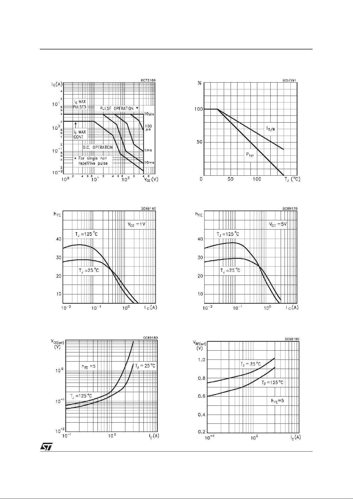
Safe OperatingAreas
DCCurrent Gain
DeratingCurve
DC Current Gain
CollectorEmitter Saturation Voltage
BaseEmitter Saturation Voltage
3/7
Page 4

BULD118D-1
InductiveFall Time InductiveStorage Time
ResistiveFall Time Resistive Load Storage Time
ReverseBiased SOA
4/7
Page 5

Figure1: Inductive LoadSwitching TestCircuit.
1) Fast electronic switch
2) Non- indu c t ive Resistor
3) Fast r ecovery rectifi er
Figure2: Resistive LoadSwitching Test Circuit.
BULD118D-1
1) Fast electronic switch
2) Non- indu c t ive Resistor
5/7
Page 6

BULD118D-1
TO-251 (IPAK) MECHANICAL DATA
DIM.
mm inch
MIN. TYP. MAX. MIN. TYP. MAX.
A 2.2 2.4 0.086 0.094
A1 0.9 1.1 0.035 0.043
A3 0.7 1.3 0.027 0.051
B 0.64 0.9 0.025 0.031
B2 5.2 5.4 0.204 0.212
B3 0.85 0.033
B5 0.3 0.012
B6 0.95 0.037
C 0.45 0.6 0.017 0.023
C2 0.48 0.6 0.019 0.023
D 6 6.2 0.236 0.244
E 6.4 6.6 0.252 0.260
G 4.4 4.6 0.173 0.181
H 15.9 16.3 0.626 0.641
L 9 9.4 0.354 0.370
L1 0.8 1.2 0.031 0.047
L2 0.8 1 0.031 0.039
6/7
A
E
==
C2
L2
B2
==
H
C
A3
A1
B6
L
B
B5
G
==
D
B3
2
13
L1
0068771-E
Page 7

BULD118D-1
Information furnished is believed tobe accurate and reliable. However,STMicroelectronics assumes no responsibility for the consequences
of use of such information nor for any infringement of patents or other rights of third parties which may result from its use. No license is
granted by implication or otherwise under any patent or patent rights of STMicroelectronics. Specification mentioned in this publication are
subject tochange without notice. This publication supersedes and replaces allinformation previously supplied.STMicroelectronics products
are not authorized foruse as critical components in life support devices or systems without express written approval of STMicroelectronics.
Australia - Brazil - Canada - China - France- Germany - Italy - Japan - Korea - Malaysia - Malta - Mexico - Morocco - TheNetherlands -
Singapore- Spain - Sweden- Switzerland- Taiwan - Thailand - United Kingdom- U.S.A.
The ST logo is a trademarkof STMicroelectronics
1998 STMicroelectronics– Printed in Italy – All Rights Reserved
STMicroelectronicsGROUP OF COMPANIES
.
7/7
 Loading...